Background
The explosive growth of the amount of information at present places higher demands on memory. The magnetoelectric random access memory is one of the most potential memories, and has advantages in stability, low power consumption and the like. In a magnetoelectric random access memory, how to effectively utilize a ferroelectric material to effectively regulate and control the magnetic moment of a ferromagnetic layer is one of important contents of research on the magnetoelectric random access memory. For this reason, there is a need to find a means to effectively characterize magnetic and electrical properties, including conductivity and piezoelectricity.
The Scanning Probe Microscope (SPM) uses the interaction force between the sample and the nanoprobe to detect the basic physical properties (such as morphology, magnetism, piezoelectricity, etc.) of the sample, and because the probe can be made to be very small in size, the SPM has very high spatial resolution when reflecting the physical properties of the sample. In a magnetoelectric random access memory, the piezoelectric, conductive areas and magnetic domains of a material generally have smaller space sizes, so that a scanning probe microscope is an important tool for researching the coupling effect between the electrical property and the magnetism of the material under the micro-nano scale.
Patent document No. CN 105510636a discloses a nano magnetic-electric-thermal multi-parameter coupling in-situ detection system and a detection method thereof, the detection system includes a scanning probe microscope platform, a probe control unit, a morphology and magnetic signal detection platform, and an electric signal detection platform, and provides a method for detecting magnetic and electric properties of a sample, specifically: firstly, fixing a sample on a scanning probe microscope platform, displacing a probe to an initial position, and adopting a contact mode, namely, controlling the point contact or vibration point contact of the probe tip and the surface of the sample, and carrying out directional scanning on the surface of the sample along the transverse direction to obtain a shape image of the sample; then, the probe returns to the initial position, a non-contact mode is adopted, namely, the probe is lifted upwards for a certain distance, the surface of the sample is scanned according to the transverse orientation, the needle point of the probe is controlled to longitudinally displace or vibrate along the topographic image in the scanning process, the displacement and/or vibration signal acquisition unit receives a longitudinal displacement signal and/or a vibration signal of the needle point of the probe, and a magnetic signal image of the sample is obtained through analysis of the central control unit; and then, the probe returns to the initial position again, and the transverse directional scanning is performed on the surface of the sample again by adopting a contact mode to obtain an electric signal image of the sample. Although the detection method is simple, the problem of multiple scanning times exists for the measurement of the magnetism and the electrical property of the material in the same micro-nano scale range, for example, directional scanning is needed when a morphology image is detected, directional scanning is needed when the magnetic property is detected, and directional scanning is also needed when the electrical property of a sample is detected, so that the scanning is complicated, the detection cost is high, and on the other hand, the sample drift is difficult to inhibit under the condition of multiple scanning, and the measurement precision is influenced.
Disclosure of Invention
In view of the above technical situation, the present invention provides a detection method for a scanning probe microscope with a magnetic-electric signal detection function, which can simplify the detection process, reduce the detection cost, and improve the detection precision.
The technical scheme provided by the invention is as follows: a probing method of a scanning probe microscope having a magnetic-electric signal probing function, the scanning probe microscope comprising:
selecting a probe with both magnetism and conductivity;
a probe control unit for driving the probe to perform displacement and vibration;
the probe signal acquisition unit is used for receiving displacement and vibration signals of the probe;
a piezoelectric electrical control unit for exciting piezoelectric properties of the sample;
and the conductive electrical control unit is used for exciting and acquiring the conductive property of the sample.
Fixing a sample on a scanning probe microscope platform, wherein the detection method comprises the following steps:
(1) the probe scans the surface of the sample transversely and directionally from the initial position, and a contact mode is adopted in the scanning process, namely, the contact between the tip of the probe and the surface point of the sample is controlled
In the scanning process, the detection process at a certain scanning point is the following a process:
the probe signal acquisition unit receives a displacement signal of the probe cantilever and acquires and analyzes a morphology signal of the sample at the scanning point; at the same time, the user can select the desired position,
when the sample has conductivity, the electric conduction electrical control unit generates an excitation electric signal, the electric signal flows into the probe and the sample to form an electric loop, and the electric conduction signal of the sample is obtained through the electric signal acquisition unit;
when the sample has piezoelectricity, the piezoelectric electricity control unit generates an alternating current signal with the frequency f and transmits the alternating current signal to the sample, the sample generates vibration with the frequency f and transmits the vibration to the probe due to the inverse piezoelectric effect, the probe signal acquisition unit receives a vibration signal with the frequency f of the probe tip, and the piezoelectric signal of the sample at the scanning point is obtained through analysis;
then, the next scanning point is entered along the transverse orientation, and the process A is repeated until the scanning is finished;
(2) when the transverse orientation scanning in the step (1) is finished, the probe returns to the initial position and adopts a non-contact mode, namely, the probe is lifted upwards for a certain distance, and the surface of the sample is scanned according to the transverse orientation
Controlling the tip of the probe to perform vibration scanning along the profile obtained in the step (1);
the detection process at a certain scanning point is the following process B:
the probe signal acquisition unit receives the vibration signal of the probe, and the magnetic signal image of the sample is obtained through acquisition and analysis.
As an implementation, a commercially available magnetic probe can be chosen for the measurement because it is both electrically conductive and magnetic.
As one implementation, the probe control unit includes a scanner, an oscillation actuator; the scanner is fixedly connected with the probe and is used for driving the probe to generate relative displacement with the sample; the oscillation actuator is used for driving the probe to vibrate longitudinally.
As one implementation, the probe signal acquisition unit comprises a light source, an optical lever system, a photoelectric detector and a signal processor; in the working state, the light source irradiates the probe arm, and the reflected signal is collected by the photoelectric detector and then processed by the signal processor. Preferably, the signal processor is connected with a controller, and the controller comprises a comparator, a PI gain control and a high-voltage amplifier; the signal is fed back to the oscillation actuator through the signal processor and the controller to form a closed-loop control system. As a further preference, the controller is connected with the piezoelectric electrical control unit; the controller is connected with the conductive electrical control unit.
As one implementation, a piezoelectric electrical control unit for exciting a piezoelectric property of a sample includes an alternating current voltage source and a direct current voltage source. The piezoelectric electrical control unit applies a voltage to the sample through the probe tip for excitation of the piezoelectric signal and polarization of the sample.
In one implementation, the electrically conductive electrical control unit includes a direct current voltage source and an ammeter. Wherein the current meter is connected in series with a voltage source, the electrically conductive electrical control unit applies a voltage to the sample through the probe tip, and the current in the sample is read by the current meter.
The invention simultaneously obtains the morphology signal and the conductive signal and/or the piezoelectric signal of the sample by utilizing the contact mode in the primary scanning process, then carries out the secondary scanning, and obtains the magnetic signal of the sample by utilizing the non-contact mode. Compared with the prior art, the detection method simplifies the detection process, efficiently realizes the characterization of the electrical characteristics (including the conductive characteristics and the piezoelectric characteristics) and the magnetism of the sample, reduces the detection cost and improves the detection precision.
In addition, the inventor finds that in the simplified detection method, when the electrical characteristics of the sample are measured, electric charges are inevitably introduced to the sample, and then an electrostatic potential is introduced to the surface of the sample, and since the magnetic force and the electrostatic force are long-range forces and the acting forces are similar, the electrostatic force interferes the magnetic signal measurement to different degrees in the process of measuring the magnetic signal, so that the result of measuring the magnetic signal is inaccurate. In order to solve the above problems, the present inventors have conducted trial and error and found that a method of eliminating the electrostatic force disturbance is as follows:
the main reason for the electrostatic force interference is the potential difference V between the probe and the sample surface
tsIt is therefore necessary to eliminate the potential difference between the probe and the sample surface at the same time as the magnetic signal measurement, for which purpose the potential difference V between the probe and the sample is eliminated with a kelvin control system
tsThe principle is as follows: the probe is raised to a specific height from the sample surface, and a Kelvin control unit energizes an alternating voltage V between the probe and the sample
ωIf the probe and sample are considered to be the two plates of a parallel plate capacitor (capacitance C), respectively, then the presence of a force between the probe and sample can be expressed as:
a frequency multiplication component thereof
And V
tsDirectly related, this force causes the probe to vibrate at a frequency ω. To this end, the Kelvin controller applies a DC bias voltage V between the probe and the sample
dcAnd obtaining vibration information S with the probe vibration frequency omega through a vibration signal acquisition unit
ωThe DC bias voltage V is controlled by a Kelvin controller
dcWhen V is
dcAnd V
tsWhen equal, the force between the probe and the sample
Zero, vibration at probe frequency ω disappears (S)
ω0) when the probe is at an equal potential to the sample surface, the magnetic signal measured on this basis will avoid interference from the electrostatic potential of the sample surface.
That is, the kelvin controller is introduced into the scanning probe microscope system to eliminate the electrostatic force, so that the interference of the electrostatic potential on the surface of the sample is effectively avoided in the measurement of the magnetic signal, and the test accuracy is improved, and the specific method comprises the following steps:
the scanning probe microscope further comprises a Kelvin control unit, wherein the Kelvin control unit comprises an alternating voltage applying unit and a Kelvin controller; the device comprises an alternating current voltage source, a probe needle point, a Kelvin controller, a photoelectric detector, a feedback signal source and a feedback signal source, wherein the alternating current voltage source applies alternating current excitation voltage to a sample through the probe needle point to cause local fluctuation of the sample, the fluctuation of the surface of the sample is received and processed by the photoelectric detector and fed back to the Kelvin controller, the Kelvin controller outputs a feedback direct current voltage, and the direct current voltage is superposed with the alternating current voltage signal;
in the step (2), in the non-contact scanning process, the probe vibrates at a frequency v under the action of the probe control unit; the Kelvin control unit applies an alternating voltage V between the probe and the sampleωThe probe generates vibration with frequency omega under the action of electrostatic force, and simultaneously, a Kelvin controller feeds back a direct-current voltage VdcApplied between the probe and the sample; the probe signal acquisition unit receives a vibration signal with the frequency omega of the probe, and adjusts the direct-current voltage V under the action of the Kelvin controllerdcOf the probeAnd the vibration amplitude with the frequency omega is zero, and the vibration with the frequency v of the probe is collected and analyzed at the moment to obtain the magnetic signal of the sample.
As one realization mode, the other path of the signal processor is connected with a Kelvin control system, and the Kelvin controller is connected with the probe to form a feedback loop.
To improve the accuracy of the test, the measurement is usually selected near the resonance frequency of the probe, and to avoid interference between the electrostatic force test and the magnetic measurement, the frequency ω of the KPFM test is usually selected near twice the eigen-vibration frequency of the probe, while the frequency ν of the MFM test is selected near one time the eigen-vibration frequency of the probe.
In the above-described embodiment, the vibration amplitude of the probe at the frequency ω is used as the feedback signal, and the change in the resonance frequency of the probe may be used as the feedback signal, and the basic principle is as follows:
the probe can be equivalent to a spring oscillator, and the resonance frequency of the spring oscillator satisfies F ═ k delta x
Where k is the equivalent elastic coefficient and m is the equivalent mass. Under the action of external forces such as electrostatic force, magnetic force and the like, the resonance frequency of the probe can change:
during the measurement of KPFM, a frequency ω is applied between the probe and the sample
1And a DC voltage V regulated by a Kelvin controller
dcThen the shift of the resonant frequency of the probe under the action of the electrostatic force and the magnetic force is approximately:
it is shown that the resonance frequency of the probe is shifted and modulated by the electrostatic and magnetic forces. By analysing the change in the probe vibration frequency, the modulation of the probe vibration frequency is eliminated, when V is
dc=V
tsSample(s)The electrostatic potential of the surface is compensated by a dc bias. In addition, due to V
acUsually a small amount which causes a negligible change in the resonant frequency of the probe, where the change in the vibrational frequency of the probe reflects primarily information from the sample magnetism. Therefore, the method can greatly eliminate the interference of the electrostatic potential on the magnetic domain measurement, thereby improving the accuracy of the magnetic measurement. During actual operation, ω
1A smaller frequency. Namely, the specific method is as follows:
in the step (2), in the non-contact scanning process, the probe has a resonance frequency v under the action of the probe control unit1Vibration of (2); the Kelvin control unit applies a frequency omega between the probe and the sample1Ac voltage V ofω1The resonance frequency of the probe is shifted and modulated by electrostatic force, and a DC voltage V is applied between the probe and the sample by a Kelvin controllerdcRegulating the DC voltage VdcAnd eliminating the vibration frequency modulation signal of the probe, collecting and analyzing the vibration signal of the probe, and obtaining the magnetic signal of the sample.
Detailed Description
The present invention will be described in further detail with reference to the following embodiments, which are not intended to limit the invention, but are to facilitate understanding of the invention.
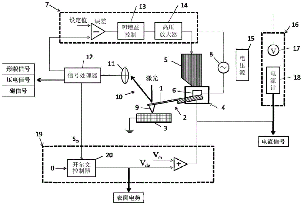
In this embodiment, the structure of the main part of the scanning probe microscope is shown in fig. 1. Scanning probe microscopy uses a probe 2 comprising a probe cantilever 1 to probe properties of a sample 3. The probe 2 is fixed to the scanner 5 by a probe holder 4. The probe holder 4 has an oscillating actuator 6, the probe is mechanically coupled to the oscillating actuator 6, and the oscillating actuator 6 causes the probe 2 to oscillate at a frequency close to its cantilever resonance. The role of the scanner 5 is to produce relative displacement between the probe and the sample, the scanner 5 typically comprising a plurality of actuators and generating mutually orthogonal movements in the three directions X-Y-Z.
Under the control of the controller 7, an alternating voltage signal is applied from the alternating signal source 8, so that the oscillation actuator 6 drives the probe 2 to vibrate, the probe tip 9 interacts with the sample to cause the morphological characteristics of the cantilever 1 to change, and the information of the surface of the sample 3 is reflected by detecting the change of the morphological characteristics of the cantilever 1.
In fig. 1, a laser beam is irradiated on a cantilever 1 by using a photo-lever system 10 to detect the morphological feature of the cantilever 1, the reflected beam is reflected to a photo-detector 11, received and processed by a signal processing system 12, and the signal is transmitted to a controller 7. The controller compares the signal to a set point, determines the difference between the set point and the signal value, i.e. the difference reflecting the interaction, and then generates a control signal via the PID gain control module 13 to maintain a relatively constant interaction between the probe 2 and the sample 3, determining the error. The control signal is typically amplified by a high voltage amplifier 14 before driving the scanner 5.
When the sample 3 itself has piezoelectricity, the piezoelectric electrical control unit 15 applies an alternating voltage to the sample 3 through the probe 2 to cause dynamic changes of the local shape of the sample, and the dynamic changes are amplified by the optical lever system 10, extracted and analyzed to obtain a piezoelectric signal of the sample, and the piezoelectric electrical control unit 15 is a voltage source. The voltage source can also provide a dc voltage to electrically polarize the sample 3.
The scanning probe microscope further comprises a conductive electrical control unit 16, the conductive electrical control unit 16 comprises an electrical signal applying unit and an electrical signal collecting unit, when the sample 3 itself has conductivity, the electrical signal applying unit excites an electrical signal, the electrical signal flows into the probe and the sample,an electrical loop is formed, and the conductive signal of the sample is obtained through the electrical signal acquisition unit. In fig. 1, the electric signal applying unit is a voltage source 17, and the electric signal collecting unit is an ammeter 18. In fig. 1, the scanning probe microscope further includes a kelvin control unit 19 for eliminating the electrostatic force, including an alternating voltage applying unit and a kelvin controller 20. The Kelvin controller 20 is based on the feedback signal SωRegulating the output DC voltage VdcSo that the feedback signal SωIs zero.
Example 1:
in this example, the scanning probe microscope is shown in FIG. 1, and the probe is a commercial MESP probe with both conductivity and magnetism selected from SrTiO3CoFe grown on a substrate2O4A magnetic thin film was used as a sample. Fixing the sample on the scanning probe microscope platform, and using the scanning probe microscope to carry out CoFe2O4The process of characterizing the morphology, conductivity and magnetic domains of the thin film is as follows:
(1) under the action of the scanner 5, the probe carries out directional scanning on the surface of the sample from an initial position, and a contact mode is adopted in the scanning process, namely, the tip of the probe is controlled to be in point contact with the surface of the sample
In the scanning process, the detection process at a certain scanning point is the following a process:
the change of the bending state of the probe cantilever 1 is detected by the optical lever system 10 entering the photodetector 11, received and processed by the signal processing system 12 and then transmitted to the controller 7. The controller 7 compares the signal with a set bending value of the cantilever 1, determines a difference between the set value and the signal value, i.e. reflects the topographic feature of the sample at the point, and then generates a control signal via the PID gain control module 13, which is amplified by the high voltage amplifier 14 and controls the scanner 5 to maintain the cantilever 1 with the set bending degree. Meanwhile, a voltage source 17 applies a certain voltage on the probe, the electric signal flows into the probe and the sample to form an electric loop, the current is read by an ammeter 18, and CoFe is obtained2O4The conductive information of the film.
Then, the next scanning point is entered in the lateral orientation, and the above a process is repeated until the scanning is finished.
(2) When the transverse orientation scanning in the step (1) is finished, the probe returns to the initial position under the action of the scanner 5, and the lifting scanning is carried out on the surface of the sample according to the transverse orientation in the step (1) by adopting a non-contact mode, namely the probe is lifted upwards for a certain distance, for example, 100 nanometers
And (3) in the scanning process, controlling the probe tip to move along the profile obtained in the step (1).
The detection process at a certain scanning point is the following process B:
an AC voltage applying unit in the controller 19 applies an AC voltage V of 450kHz (around the probe double-frequency eigenresonance frequency) between the probe and the sampleωThe probe generates vibration with a frequency of 450kHz under the action of electrostatic force, and a DC voltage V is applied between the probe and the sample through a Kelvin controller 20dcRegulating the DC voltage VdcThe amplitude of the signal with the frequency of 450kHz obtained by the photoelectric detector 11 is made zero; meanwhile, the probe vibrates at the frequency 73kHz of the first-frequency eigenresonance frequency under the action of the oscillation actuator 6, and magnetic signals of the sample at the scanning point are obtained by detecting and analyzing the vibration and phase information of the probe with the frequency 73 kHz.
Then, the next scanning point is entered in the transverse orientation, and the above B process is repeated until the scanning is finished.
Example 2:
in this example, the scanning probe microscope is shown in FIG. 1, and the probe is a commercial MESP probe with both conductivity and magnetism selected from SrTiO3BiFeO with self-assembly characteristic grows on substrate3-CoFe2O4The film was used as a sample. Fixing a sample on the scanning probe microscope platform, and utilizing the scanning probe microscope to measure the shape of the film and BiFeO3Piezoelectric and CoFe2O4The process of characterizing the magnetic domain of (a) is as follows:
(1) under the action of the scanner 5, the probe carries out directional scanning on the surface of the sample from an initial position, and a contact mode is adopted in the scanning process, namely, the tip of the probe is controlled to be in point contact with the surface of the sample
In the scanning process, the detection process at a certain scanning point is the following a process:
the change of the bending state of the probe cantilever 1 is detected by the optical lever system 10 entering the photodetector 11, received and processed by the signal processing system 12 and then transmitted to the controller 7. The controller 7 compares the signal with a set bending value of the cantilever 1, determines the difference between the set value and the signal value, and the error is amplified by the high voltage amplifier 14 to control the scanner 5 via the PID gain control module 13 to maintain the cantilever 1 at the set bending level. Meanwhile, a voltage source 15 applies an alternating voltage with the frequency of 23kHz to the sample 3 through the probe 2, the vibration with the frequency of 23kHz generated by the sample due to the piezoelectric effect is transmitted to the probe cantilever 1, the signal is received and processed by a photoelectric detector 11 through an optical lever system 10, and CoFe is obtained through analysis2O4Piezoelectric information of the film sample at the scanning point.
Then, the next scanning point is entered along the scanning direction, and the process a is repeated until the scanning is finished.
(2) When the directional scanning in step (1) is finished, the probe returns to the initial position under the action of the scanner 5, and the non-contact mode is adopted, namely, the probe is lifted upwards for a certain distance, for example, 100 nanometers, and the surface of the sample is lifted and scanned according to the scanning direction in step (1)
And (3) in the scanning process, controlling the probe tip to move along the profile obtained in the step (1).
The detection process at a certain scanning point is the following process B:
the probe is vibrated at its eigenresonance frequency of 73kHz by the oscillating actuator 6. An alternating voltage applying unit in the Kelvin control unit 19 applies an alternating voltage V having a frequency of 3kHz between the probe and the sampleωThe resonant frequency of the probe is shifted and modulated by the electrostatic force. Applying a DC voltage V between the probe and the sample by means of a Kelvin controller 20dcRegulating the DC voltage VdcThe vibration frequency modulation signal of the probe obtained by the photoelectric detector 11 disappears; meanwhile, the magnetic signal of the sample at the scanning point is obtained by detecting and analyzing the vibration information of the probe.
Then, the next scanning point is entered in the transverse orientation, and the above B process is repeated until the scanning is finished.
The embodiments described above are intended to illustrate the technical solutions of the present invention in detail, and it should be understood that the above-mentioned embodiments are only specific embodiments of the present invention, and are not intended to limit the present invention, and any modification, supplement or similar substitution made within the scope of the principles of the present invention should be included in the protection scope of the present invention.