Background
The microwave reconfigurable device plays an important role in establishing an intelligent wireless communication network and promoting the development of a 5G communication technology. However, if only a single regulating and controlling mechanism is used in a fixed frequency position, the existing microwave reconfigurable device can only control the amplitude of the output microwave signal or only control the phase of the output microwave signal, which greatly limits the application scenarios of the microwave reconfigurable device. Although the amplitude and the phase of the output microwave signal can be simultaneously controlled by using a plurality of regulating mechanisms, the structure is complex and the manufacturing cost is high; and the plurality of regulating mechanisms can consume more microwave energy, so that the working efficiency of the microwave reconfigurable device is reduced.
Disclosure of Invention
In view of the above problems in the prior art, embodiments of the present disclosure provide a microwave amplitude and phase controller and a method for controlling microwave amplitude and/or phase, so as to achieve simultaneous control of microwave amplitude and phase on the premise of simplifying a structure, reducing cost, and improving work efficiency.
In order to achieve the purpose, the embodiment of the disclosure adopts the following technical scheme:
in a first aspect, embodiments of the present disclosure provide a microwave amplitude and phase controller, including: the first substrate and the second substrate are oppositely arranged; the conducting layer and the first alignment film are sequentially arranged on one surface, facing the second substrate, of the first substrate, and the conducting layer is configured to receive a first voltage signal; the resonance structure layer and the second alignment film are sequentially arranged on one surface, facing the first substrate, of the second substrate, and the resonance structure layer is configured to receive a second voltage signal and is configured to transmit a microwave signal; and the liquid crystal layer is arranged between the first substrate and the second substrate.
In the microwave amplitude phase controller, a conducting layer and a resonance structure layer are respectively arranged on the upper side and the lower side of the liquid crystal layer, and the pressure difference between the conducting layer and the resonance structure layer is adjustable; and the upper and lower sides of the liquid crystal layer are respectively provided with a first alignment film and a second alignment film for aligning liquid crystal molecules. When the voltage difference between the conductive layer and the resonance structure layer is changed, liquid crystal molecules are deflected, and thus the equivalent dielectric constant of the liquid crystal layer is changed. When the microwave amplitude and phase controller is adopted to control microwaves, the microwaves are input into the resonant structure layer, resonance is generated in the resonant structure layer, meanwhile, the equivalent dielectric constant of the liquid crystal layer can influence the resonance effect, so that the amplitude and the phase of the microwaves are influenced, the liquid crystal molecules are deflected to different degrees by adjusting the pressure difference applied to the liquid crystal layer, the equivalent dielectric constant of the liquid crystal layer is caused to generate different changes, different influences are generated on the resonance in the resonant structure layer, the amplitude and the phase of the microwaves are changed differently, the microwaves with required amplitude and phase can be finally obtained, and the simultaneous control on the amplitude and the phase of the microwaves is realized.
Compared with the existing device for simultaneously controlling the amplitude and the phase of the microwave, the microwave amplitude and phase controller has the advantages of simple structure, low manufacturing cost and high working efficiency.
Based on the above technical solution, optionally, the resonant structure layer includes: the composite resonance structure comprises a gap capacitor and a cross-over conductive structure connected in parallel with two ends of the gap capacitor; the first signal line and the second signal line are respectively electrically connected with two ends of the gap capacitor, the first signal line is used for receiving a microwave signal to be regulated, and the second signal line is used for outputting the regulated microwave signal.
Optionally, the composite resonant structure further includes: the gap capacitor comprises a first connecting line and a second connecting line, wherein one end of the gap capacitor is electrically connected with one end of the cross-over conductive structure and the first signal line through the first connecting line, and the other end of the gap capacitor is electrically connected with the other end of the cross-over conductive structure and the second signal line through the second connecting line.
Optionally, the gap capacitor includes two opposite metal strips arranged at an interval, and the two metal strips of the gap capacitor have the same length and width; the bridging conductive structure is a metal strip and is an axisymmetric structure.
Optionally, the metal strip of the slot capacitor is perpendicular to the first connection line and the second connection line.
Optionally, the two metal strips of the slot capacitor are symmetrically arranged with respect to the symmetry axis of the bridging conductive structure.
Optionally, the length of the metal strip bridging the conductive structure is less than or equal to 0.5 λ; wherein λ is the operating wavelength of the microwave to be regulated.
Optionally, the gap capacitor includes two opposite metal electrodes arranged at an interval, and the metal electrodes are interdigital metal electrodes.
Optionally, an orthographic projection of the liquid crystal layer on the first substrate at least covers an orthographic projection of the gap capacitor on the first substrate.
Optionally, the thickness of the liquid crystal layer is less than or equal to 0.5 λ; wherein λ is the operating wavelength of the microwave to be regulated.
Optionally, the microwave amplitude and phase controller further includes: the liquid crystal display panel comprises a frame arranged between a first substrate and a second substrate, wherein the frame is matched with the first substrate and the second substrate to form a cavity, and the liquid crystal layer is filled in the cavity.
Optionally, the alignment directions of the first alignment film and the second alignment film are the same.
Optionally, the conductive layer is grounded.
In a second aspect, embodiments of the present disclosure provide a method for controlling amplitude and/or phase of microwaves, the method comprising: connecting a first voltage signal into a conductive layer of a microwave amplitude phase controller, and connecting a second voltage signal into a resonance structure layer of the microwave amplitude phase controller; wherein the microwave amplitude phase controller is the microwave amplitude phase controller according to the first aspect; and inputting a microwave signal to be regulated to a resonant structural layer of the microwave amplitude-phase controller, and regulating the voltage difference between the first voltage signal and the second voltage signal until the regulated microwave signal output by the resonant structural layer has the required amplitude and/or phase.
The beneficial effects produced by the above method for controlling the amplitude and/or phase of the microwave are the same as those of the microwave amplitude and phase controller provided in the first aspect, and are not described herein again.
Detailed Description
In order to make the aforementioned objects, features and advantages of the present disclosure more comprehensible, embodiments accompanying figures are described in detail below. It is to be understood that the described embodiments are merely illustrative of some, and not restrictive, of the embodiments of the disclosure. All other embodiments, which can be derived by a person skilled in the art from the embodiments disclosed herein without making any creative effort, shall fall within the protection scope of the present disclosure.
In the embodiment of the present disclosure, a plane in which the microwave amplitude and phase controller 100 is located (which may also be regarded as a plane in which the first substrate 1 or the second substrate 2 is located) is an XOY plane, and in the XOY plane, an X direction and a Y direction are two directions perpendicular to each other; the direction perpendicular to the XOY plane and directed from the first substrate 1 to the second substrate 2 is the Z direction.
An embodiment of the present disclosure proposes a microwave amplitude and phase controller, as shown in fig. 1 and 2, the microwave amplitude and phase controller 100 including: a first substrate 1 and a second substrate 2 disposed opposite to each other; the conductive layer 3 and the first alignment film 5 are sequentially arranged on one surface of the first substrate 1 facing the second substrate 2; the resonance structure layer 4 and the second alignment film 6 are sequentially arranged on one surface, facing the first substrate 1, of the second substrate 2; and a liquid crystal layer 8 disposed between the first substrate 1 and the second substrate 2.
In the microwave amplitude-phase controller 100, the conductive layer 3 is configured to receive a first voltage signal, the resonant structure layer 4 is configured to receive a second voltage signal, and the first voltage signal and/or the second voltage signal are/is adjustable, so that a voltage difference between the first voltage signal and the second voltage signal is adjustable.
The resonant structure layer 4 is configured to transmit a microwave signal. Illustratively, the resonant structure layer 4 has a microwave signal input end and a microwave signal output end, the microwave signal input end is used for receiving a microwave signal, and the microwave signal output end is used for outputting the microwave signal.
In the microwave amplitude phase controller 100, the conductive layer 3 and the resonant structure layer 4 are respectively arranged on the upper side and the lower side of the liquid crystal layer 8, and the pressure difference between the two layers is adjustable; and the upper and lower sides of the liquid crystal layer 8 are also respectively provided with a first alignment film 5 and a second alignment film 6 to align the liquid crystal molecules. When the voltage difference between the conductive layer 3 and the resonant structure layer 4 is changed, liquid crystal molecules are deflected, and thus the equivalent dielectric constant of the liquid crystal layer 8 is changed.
When the microwave amplitude and phase controller 100 is used for controlling microwaves, the microwaves are input into the resonant structure layer 4, the resonant structure in the resonant structure layer 4 is caused to generate resonance, meanwhile, the equivalent dielectric constant of the liquid crystal layer 8 can influence the resonance effect, so that the amplitude and the phase of the microwaves are influenced, the liquid crystal molecules are deflected to different degrees by adjusting the pressure difference applied to the liquid crystal layer 8, the equivalent dielectric constant of the liquid crystal layer 8 is caused to generate different changes, the resonance in the resonant structure layer 4 is influenced differently, the amplitude and the phase of the microwaves can be changed differently, the microwaves with required amplitude and phase can be obtained finally, and the simultaneous control of the amplitude and the phase of the microwaves is realized.
Compared with the existing device for simultaneously controlling the amplitude and the phase of the microwave, the microwave amplitude and phase controller 100 provided by the embodiment can simultaneously control the amplitude and the phase of the microwave without using a plurality of regulating and controlling mechanisms, has a very simple structure and low manufacturing cost, does not consume too much microwave energy, and therefore has higher working efficiency.
In addition, by designing the internal structure of the microwave amplitude and phase controller 100 and changing the operating frequency of the microwave amplitude and phase controller 100, the microwave amplitude and phase controller 100 can achieve different effects of changing only the phase of the microwave, or changing the amplitude of the microwave, or simultaneously changing the amplitude and the phase of the microwave, that is, the microwave amplitude and phase controller 100 can be used as an amplitude controller alone, a phase controller (i.e., a phase shifter) alone, or both an amplitude controller and a phase shifter.
In the microwave amplitude and phase controller 100, the structural design of the resonant structural layer 4 is important to the effect of the amplitude and phase control, and some possible designs are given below as examples.
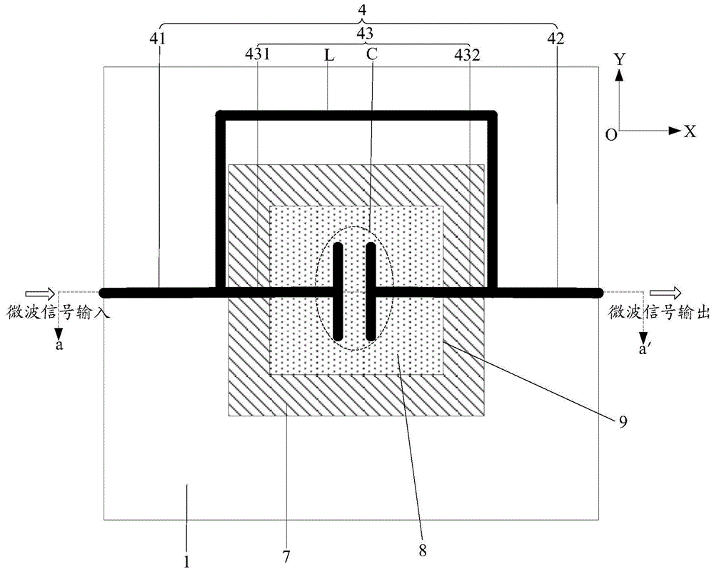
Referring to fig. 1, the resonant structure layer 4 includes: a composite resonant structure 43, a first signal line 41 and a second signal line. Wherein:
the composite resonant structure 43 includes a slot capacitor C and a cross-over conductive structure L connected in parallel to two ends of the slot capacitor C. When microwave is input, the microwave can cause the gap capacitor C to be coupled to generate resonance, the resonance effect on the gap capacitor C can induce the cross-over conductive structure L, and the cross-over conductive structure L can adversely affect the resonance on the gap capacitor C, so that the whole composite resonance structure 43 generates a resonance effect with a very high quality factor.
The first signal line 41 and the second signal line 42 are respectively disposed at two ends of the slot capacitor C and electrically connected to the two ends of the slot capacitor C. The first signal line 41 serves as a microwave signal input end of the resonant structure layer 4, that is, a microwave signal input end of the entire microwave amplitude-phase controller 100, and is configured to receive a microwave signal to be regulated. The first signal line 42 serves as a microwave signal output end of the resonant structure layer 4, that is, a microwave signal output end of the entire microwave amplitude-phase controller 100, and is configured to output a regulated microwave signal.
The composite resonant structure 43 further comprises: one end of the gap capacitor C is electrically connected to one end of the cross-over conductive structure L and the first signal line 41 through the first connection line 431, and the other end of the gap capacitor C is electrically connected to the other end of the cross-over conductive structure L and the second signal line 42 through the second connection line 432.
As a possible design, please continue to refer to fig. 1, the slot capacitor C includes two metal strips that are opposite and spaced apart from each other, and the two metal strips of the slot capacitor C have the same length and the same width; the bridging conductive structure L is a metal strip and is an axisymmetric structure; further, the first connecting line 431 and the second connecting line 432 have the same length and the same width; the metal strip of the slot capacitor C is perpendicular to the first connection line 431 and the second connection line 432; the two metal strips of the slot capacitor C are symmetrically arranged with respect to the symmetry axis of the bridging conductive structure L; so that the composite resonance structure 43 formed by the gap capacitor C, the cross-over conductive structure L, the first connection line 431 and the second connection line 432 has an axisymmetric structure, which is beneficial to enhancing resonance and improving quality factor.
For each dimension design of the resonant structure layer 4, microwave amplitude and phase controllers 100 with different dimension specifications, working frequency requirements and the like should have different dimension design schemes.
For example, taking the structure of the resonant structure layer 4 shown in fig. 1 as an example, it is assumed that one set of sides of the liquid crystal layer 8 in the microwave amplitude-phase controller 100 is parallel to the X direction and the other set of sides is parallel to the Y direction. The metal strips of the slot capacitances C of the composite resonant structure 43 in the resonant structure layer 4 are parallel to the Y-direction. Referring to fig. 3, the following design can be adopted for each dimension parameter (in the following description, it is assumed that the operating wavelength of the microwave to be modulated input to the microwave amplitude and phase controller 100 is λ):
the length x1 (the sum of the lengths of the part parallel to the x direction and the parts parallel to the Y direction on two sides) of the bridging conductive structure L is less than or equal to 1 lambda, optionally less than or equal to 0.5 lambda, and the width d1 is less than or equal to 0.5 lambda;
the length x2 of the metal strip of the gap capacitor C is less than or equal to 0.5 lambda, the width d2 of the metal strip of the gap capacitor C is less than or equal to 0.5 lambda, and the gap d3 between the two metal strips is less than or equal to 0.5 lambda;
the length x3 of the first signal line 41 and the second signal line 42 is less than or equal to 0.5 lambda, and the width d3 is less than or equal to 0.5 lambda.
In another embodiment, referring to fig. 4, the slot capacitor C may include two opposing metal electrodes spaced apart from each other, and the metal electrodes are interdigitated metal electrodes.
In the embodiment of the present disclosure, the materials of the conductive layer 3 and the resonance structure layer 4 are conductive materials; further, the materials of the two are metals, such as: gold, silver, copper, aluminum, and the like. The wire for supplying the first voltage signal may be connected to an arbitrary position on the conductive layer 3, and the wire for supplying the second voltage signal may be connected to an arbitrary position on the resonance structure layer 4.
The thickness of the conductive layer 3 and the resonant structure layer 4 can be less than or equal to 0.5 lambda.
The preparation process of the conductive layer 3 may be: the conductive layer material is adopted to carry out the processes of evaporation, coating, printing or deposition and the like to form a whole layer of conductive film. The preparation process of the resonant structure layer 4 may be: firstly, a whole layer of film with designed thickness is formed by using the resonance structure material, then a specific part in the formed film is removed by using a photoetching process, and the remaining part forms a required resonance structure layer 4 pattern.
In some embodiments, the conductive layer 3 may be grounded, that is, the first voltage signal connected to the conductive layer 3 is a ground voltage, so that the potential of the conductive layer 3 may be fixed, and when the voltage difference between the conductive layer 3 and the resonant structure layer 4 is adjusted, only the second voltage signal connected to the resonant structure layer 4 may be adjusted, which simplifies the operation.
The alignment directions of the first alignment film 5 and the second alignment film 6 are uniform so that the liquid crystal molecules in the liquid crystal layer 8 have uniform alignment. The alignment directions of the first alignment film 5 and the second alignment film 6, i.e., the orientations of the liquid crystal molecules in the liquid crystal layer 8 (the orientations described herein refer to the orientations of the long axes of the liquid crystal molecules), may be along the positive and negative directions of the X axis, or along the positive and negative directions of the Y axis, or along any other directions on the XOY plane.
The liquid crystal display device comprises a frame 7 arranged between the first substrate 1 and the second substrate 2, wherein the frame 7 is matched with the first substrate 1 and the second substrate 2 to form a cavity 9 for containing liquid crystal to be measured, the frame 7 is used for preventing the liquid crystal from leaking, maintaining a gap between the first substrate 1 and the second substrate 2 and providing a supporting space for the liquid crystal clamped between the first substrate 1 and the second substrate 2.
The thickness of the liquid crystal layer 8 may be in a range of 0.5 λ or less. The liquid crystal material can be nematic liquid crystal.
The value range of the dielectric constant of the first substrate 1 and the second substrate 2 can be 1.1-20, and can be 4.
Referring to fig. 1 and fig. 2 again, the microwave amplitude and phase controller 100 provided in the embodiment of the present disclosure may further include: and the frame 7 is arranged between the first substrate 1 and the second substrate 2, the frame 7 is matched with the first substrate 1 and the second substrate 2 to form a cavity 9, and the liquid crystal layer 8 is filled in the cavity 9. The frame 7 functions to prevent liquid crystal molecules in the liquid crystal layer 8 from leaking, maintain a gap between the first substrate 1 and the second substrate 2, and provide a supporting space for the liquid crystal layer 8 sandwiched between the first substrate 1 and the second substrate 2. The frame 7 can be made of frame sealing glue.
As a possible design, the orthographic projection of the liquid crystal layer 8 on the first substrate 1 at least covers the orthographic projection of the slot capacitor C on the first substrate 1, so that the equivalent dielectric constant of the liquid crystal layer 8 can have a relatively sufficient influence on the resonance effect on the slot capacitor C, thereby sufficiently influencing the microwaves transmitted in the composite resonance structure 43.
The above is an explanation of the structure of the microwave amplitude and phase controller 100 provided in the present disclosure, and a method for controlling the amplitude and/or phase of the microwave by using the above microwave amplitude and phase controller 100 will be described below.
It should be noted that the microwave amplitude and phase controller 100 in the present embodiment has different operating frequencies and different control effects on microwaves. Specifically, when the operating frequency of the microwave amplitude-phase controller 100 is a certain frequency, it can simultaneously generate a regulating effect on the amplitude and phase of the microwave; when the working frequency of the microwave amplitude-phase controller 100 is another frequency, it can only regulate and control the amplitude of the microwave; when the operating frequency of the microwave amplitude-phase controller 100 is another frequency, it can only regulate the phase of the microwave. In practical applications, the internal structure of the microwave amplitude and phase controller 100 is adjusted, for example: the length, width, shape, etc. of the cross-over conductive structure L are adjusted and optimized, the length, width, shape, gap between two metal electrodes, etc. of the metal electrode of the slot capacitor C are adjusted and optimized, the coverage area of the liquid crystal layer 8 is adjusted, etc., so as to achieve the purpose of adjusting the working frequency of the microwave amplitude-phase controller 100.
Referring to fig. 5, an embodiment of the present disclosure provides a method for controlling amplitude and phase of microwave, where the method includes the following steps:
s11: the first voltage signal is connected to the conductive layer 3 of the microwave amplitude and phase controller 100 provided in the embodiment of the present disclosure, and the second voltage signal is connected to the resonant structural layer 4 of the microwave amplitude and phase controller 100.
S12: inputting a microwave signal to be regulated to the resonant structural layer 4 of the microwave amplitude-phase controller 100, and adjusting a voltage difference between the first voltage signal and the second voltage signal to change an equivalent dielectric constant of the liquid crystal layer 8, thereby affecting the amplitude and the phase of the microwave until the regulated microwave signal output by the resonant structural layer 4 has the required amplitude and phase.
Before the above method steps are performed, the internal structure of the microwave amplitude and phase controller 100 needs to be designed in advance so that the operating frequency is suitable for the case of controlling the amplitude and phase of the microwave at the same time.
Referring to fig. 6, an embodiment of the present disclosure provides a control method of a microwave phase, where the control method includes the following steps:
s21: the first voltage signal is connected to the conductive layer 3 of the microwave amplitude and phase controller 100 provided in the embodiment of the present disclosure, and the second voltage signal is connected to the resonant structural layer 4 of the microwave amplitude and phase controller 100.
S22: inputting a microwave signal to be regulated to the resonant structural layer 4 of the microwave amplitude-phase controller 100, and adjusting a voltage difference between the first voltage signal and the second voltage signal to change an equivalent dielectric constant of the liquid crystal layer 8 to influence a phase of the microwave until the regulated microwave signal output by the resonant structural layer 4 has a required phase.
Before the above method steps are performed, the internal structure of the microwave amplitude and phase controller 100 needs to be designed in advance so that the operating frequency is suitable for the case where only the phase of the microwave is controlled.
Referring to fig. 7, an embodiment of the present disclosure provides a method for controlling microwave amplitude, where the method includes the following steps:
s31: the first voltage signal is connected to the conductive layer 3 of the microwave amplitude and phase controller 100 provided in the embodiment of the present disclosure, and the second voltage signal is connected to the resonant structural layer 4 of the microwave amplitude and phase controller 100.
S32: inputting a microwave signal to be regulated to the resonant structural layer 4 of the microwave amplitude-phase controller 100, and adjusting a voltage difference between the first voltage signal and the second voltage signal to change an equivalent dielectric constant of the liquid crystal layer 8 to influence the amplitude of the microwave until the regulated microwave signal output by the resonant structural layer 4 has a required amplitude.
Before the above method steps are performed, the internal structure of the microwave amplitude and phase controller 100 needs to be designed in advance so that the operating frequency is suitable for controlling the amplitude of the microwave.
As an example, a simulation model is built with the structure shown in fig. 1 and 3, assuming that the dielectric constant of the first substrate 1 and the second substrate 2 is 4 in the microwave amplitude phase controller 100; the thickness of the liquid crystal layer 8 is 1 mm; the length of the bridging conductive structure L parallel to the X direction is 6mm, the length parallel to the Y direction is 6mm, and the total length X1 is 18 mm; the width is 0.6 mm; the length x2 of the metal strip of the gap capacitor C is 2mm, the width d2 is 0.7mm, and the gap d3 between the two metal strips is 0.7 mm; the first signal line 41 and the second signal line 42 have a length x3 of 4mm and a width d3 of 1 mm. Through simulation, the working frequency of the microwave amplitude-phase controller 100 is adjustable between 2.5GHz and 3 GHz.
The course of change in the equivalent dielectric constant of the liquid crystal layer 8 from 2.5 to 3.3 represents the course of change in the liquid crystal molecules from a horizontal orientation (parallel to the XOY plane) to a vertical orientation (parallel to the Z axis).
Referring to fig. 8, the variation of the amplitude of the microwave output from the microwave amplitude phase controller 100 is shown when the equivalent dielectric constant of the liquid crystal layer 8 is changed from 2.5 to 3.3. A curve S1 shows the variation of the amplitude of the microwave at each operating frequency of the microwave amplitude-phase controller 100 when the liquid crystal molecules are aligned from the horizontal; the curve S2 shows the variation of the amplitude of the microwave at each operating frequency of the microwave amplitude-phase controller 100 when the liquid crystal molecules are aligned from vertical.
The amplitude change rate of the microwave is (maximum amplitude value-minimum amplitude value)/amplitude median value, and the amplitude median value is (maximum amplitude value + minimum amplitude value)/2. Under the premise that the working frequency of the microwave amplitude-phase controller 100 is constant, after the equivalent dielectric constant is changed from 2.5 to 3.3, according to the curves S1 and S2, the amplitude change rate of the microwave can be calculated to be very large and close to 100%.
For example: when the operating frequency of the microwave amplitude phase controller 100 is 2.8909 GHz: when the equivalent dielectric constant ∈ is 2.5, the amplitude of the microwave is 0.72734204 (maximum amplitude value); when the equivalent dielectric constant ∈ is 3.3, the amplitude of the microwave is 0.25685124 (minimum amplitude value). Therefore, the rate of change in the amplitude of the microwave was calculated to be 95%, which was close to 100%. This indicates that the microwave amplitude phase controller 100 has a large adjustable range for the microwave amplitude.
Referring to fig. 9, the change of the phase of the microwave output from the microwave amplitude phase controller 100 is shown when the equivalent dielectric constant of the liquid crystal layer 8 changes from 2.5 to 3.3. A curve S3 shows the change of the phase of the microwave at each operating frequency of the microwave amplitude-phase controller 100 when the liquid crystal molecules are aligned horizontally; the curve S4 shows the phase change of the microwave at each operating frequency of the microwave amplitude-phase controller 100 when the liquid crystal molecules are aligned vertically.
The absolute phase shift of the microwave is the maximum phase value-the minimum phase value. Under the premise that the working frequency of the microwave amplitude-phase controller 100 is fixed, after the equivalent dielectric constant is changed from 2.5 to 3.3, the absolute phase shift of the microwave can be calculated to reach about 50 degrees according to the curves S3 and S4.
For example: when the operating frequency of the microwave amplitude phase controller 100 is 2.7001 GHz: when the equivalent dielectric constant ∈ is 2.5, the phase of the microwave becomes-286.90065 (maximum amplitude value); when the equivalent dielectric constant ∈ is 3.3, the phase of the microwave becomes-333.60157 (minimum amplitude value). Thus, the absolute phase shift calculated for the microwave is 46.7 degrees. This means that the adjustable range of the microwave amplitude phase controller 100 for the microwave phase is not small, and a plurality of microwave amplitude phase controllers 100 can be used in a superimposed manner if a larger phase shift amount is to be obtained in practical use.
Furthermore, combining fig. 8 and 9, it is easy to find that:
when the operating frequency of the microwave amplitude and phase controller 100 is about 2.7GHz, the change of the equivalent dielectric constant of the liquid crystal layer 8 causes the amplitude and the phase of the microwave to change simultaneously, which means that when the microwave amplitude and phase controller 100 operates at about 2.7GHz, the amplitude and the phase of the microwave can change simultaneously, and the microwave amplitude and phase controller is suitable for a scene needing to control the amplitude and the phase of the microwave simultaneously.
When the operating frequency of the microwave amplitude and phase controller 100 is 2.5GHz, the change of the equivalent dielectric constant of the liquid crystal layer 8 cannot cause the amplitude of the microwave to change (see fig. 8), and can cause the phase of the microwave to change (see fig. 9), which means that when the microwave amplitude and phase controller 100 operates at 2.5GHz, only the phase of the microwave can be changed, and the microwave amplitude and phase controller is suitable for a scene in which only the phase of the microwave needs to be controlled.
As for the scenario that only the amplitude of the microwave needs to be controlled, since it is usually not concerned whether the phase changes or not when the amplitude of the microwave is controlled, when the microwave amplitude-phase controller 100 operates at more than 2.5GHz, the requirement of only controlling the amplitude of the microwave can be satisfied.
It should be noted that, in the embodiment of the present disclosure, although the electrodes used for driving the liquid crystal layer 8 are linear electrodes (i.e., electrodes in the resonant structure layer 4), effective driving of the liquid crystal can still be ensured. Referring to fig. 10, the liquid crystal molecules within the line-type electrode and its periphery can be effectively driven; in addition, the setting that the equivalent dielectric constant of the liquid crystal layer just below the linear electrode changes under the action of the driving voltage, and the liquid crystal layer at other places keeps unchanged for any driving voltage shows that the microwave amplitude and phase controller 100 in the embodiment of the disclosure can still effectively control the amplitude and/or phase of the microwave signal even under the setting through analog simulation.
The above description is only for the specific embodiments of the present disclosure, but the scope of the present disclosure is not limited thereto, and any changes or substitutions that can be easily conceived by those skilled in the art within the technical scope of the present disclosure should be covered within the scope of the present disclosure. Therefore, the protection scope of the present disclosure shall be subject to the protection scope of the claims.