Disclosure of Invention
In order to solve the problems of high antenna complexity and large overall antenna size in the prior art, the embodiment of the invention provides an antenna array and a terminal. The technical scheme is as follows:
in a first aspect, an antenna array is provided, which includes: a first antenna, a second antenna and a ground plane; the first antenna comprises a first metal frame in a terminal, the first metal frame is coplanar with the grounding plate, the first metal frame is respectively connected with the grounding plate and a first feeding point, and a gap is formed between the first metal frame and the grounding plate; the second antenna comprises a second metal frame in the terminal, the second metal frame is not coplanar with the grounding plate, the second metal frame is parallel to the grounding plate, and the second metal frame is respectively connected with the grounding plate and a second feeding point.
The first antenna provided by the embodiment of the invention comprises a first metal frame serving as a radiator, wherein the first metal frame is coplanar with the ground plate, and a gap exists between the first metal frame and the ground plate. The loop antenna can generate fundamental mode resonance with one time of wavelength at the required low frequency close to the central frequency point, and can obtain a relatively wide resonance frequency band, so that the low frequency band of the mobile terminal equipment can be covered.
Similarly, when feeding is performed at the second feeding point, a loop antenna may be formed between the ground plane and the second metal frame serving as a radiator of the second antenna, so as to generate radiation. In contrast, the second antenna element is not coplanar with the ground plane but is supported by the dielectric plate to form a loop antenna in a vertical plane. Thus, the requirement that the second antenna element be free of system ground meets the current narrow-frame or even frameless design requirements. Further, the feeding point of the second antenna element is selected at the middle portion of the top frame, thereby dividing the second antenna element into two loop antennas. By reasonably selecting the feed point and the grounding point, the matching of the resonance lengths of the two loop antennas in the second antenna component can be respectively controlled, so that reasonable resonance points are generated, and the combination of the two resonance points jointly covers the required frequency band. In addition, the second metal frame is not coplanar with the ground plate, and the second metal frame is parallel to the ground plate, so that the polarization direction of the second antenna is perpendicular to the ground plate.
Because the polarization directions of the first antenna and the second antenna are orthogonal, the electromagnetic waves radiated by the first antenna and the second antenna have small influence on each other, so that the coupling between the first antenna and the second antenna is small, the first antenna and the second antenna provided by the embodiment of the invention can avoid the coupling between the antennas on the premise of not arranging a decoupling component, thereby reducing the design complexity of the first antenna and the second antenna on one hand, and reducing the sizes of the first antenna and the second antenna on the other hand.
Optionally, two ends of the first metal frame are respectively connected to the ground plate to form a ring structure coplanar with the ground plate; the first feeding point is connected with a first feeding connection point on the first metal frame, and the distances between the first feeding connection point and two ends of the first metal frame are unequal, so that a loop antenna is formed.
In practical application, the size of the radiation section is inversely proportional to the frequency point of the radiation section generating resonance, so that when a fundamental mode resonance of one time of wavelength is required to be generated at the central frequency point of low frequency, the size of the radiation section of the first antenna generating the fundamental mode resonance needs to be larger.
Optionally, the first antenna includes two first grounding switches and two first reconfiguration switch sets, and two ends of the first metal frame are connected to the ground plane through one first grounding switch respectively; the first reconfiguration switch group is respectively arranged adjacent to two ends of the first metal frame and comprises at least one first reconfiguration switch; each of the first reconfiguration switches is connected to the first metal bezel and the ground plane, respectively.
By arranging the first grounding switch and the first reconstruction switch group and controlling the on and off of each reconstruction switch in the first grounding switch and the first reconstruction switch group, the position where the first metal frame is connected with the grounding plate can be changed, so that the size of the radiation section of the first antenna is changed, and the first antenna can work on different frequency bands according to requirements.
Optionally, the first metal frame is a U-shaped frame composed of a first left side frame, a first middle frame and a first right side frame which are connected in sequence, the first left side frame is located on the left side of the terminal, the first right side frame is located on the right side of the terminal, and the first middle frame is located at the top or the bottom of the terminal; the first feed connection point is disposed on a side of the first left side frame remote from the first center frame.
Optionally, two ends of the second metal frame are respectively connected to the ground plate; and a second feeding connection point arranged in the middle of the second metal frame is connected with the second feeding point to form a loop antenna.
Optionally, the second feeding connection point is connected to the second feeding point by a lumped inductance; the second metal frame comprises a first capacitor partition and a second capacitor partition; the first capacitor partition is located between the second feed connection point and one end of the second metal frame, and the second capacitor partition is located between the second feed connection point and the other end of the second metal frame.
The frequency point of the second antenna generating fundamental mode resonance can be reduced by arranging the lumped inductor, the first capacitor partition and the second capacitor partition, so that the size of the second antenna is objectively reduced.
Optionally, the second antenna includes two second ground switches and two second reconfiguration switch sets, and two ends of the second metal frame are connected to the ground plane through one second ground switch respectively; the second reconfiguration switch group is respectively arranged adjacent to two ends of the second metal frame and comprises at least one second reconfiguration switch; each second reconfiguration switch is respectively connected with the second metal frame and the grounding plate.
The second grounding switch and the second reconfiguration switch group are arranged, and the on-off of each second reconfiguration switch in the second grounding switch and the second reconfiguration switch group is controlled, so that the connection position of the second metal frame and the grounding plate can be changed, the size of the radiation section of the second antenna is changed, and the second antenna can work on different frequency bands according to requirements.
Optionally, the second metal frame is a U-shaped frame composed of a second left side frame, a second middle frame and a second right side frame which are sequentially arranged, the second left side frame is located on the left side of the terminal, the second right side frame is located on the right side of the terminal, and the second middle frame is located at the top or the bottom of the terminal;
the second feed connection point is located in the middle of the second middle rim.
Optionally, the first capacitor partition is arranged between the second left side frame and the second middle frame; and the second capacitor partition is arranged between the second right side frame and the second middle frame.
In a second aspect, a terminal is provided, which includes the antenna array of any one of the above first aspects.
The technical scheme provided by the embodiment of the invention has the following beneficial effects:
the first metal frame serving as the first antenna radiator is coplanar with the ground plate, the second metal frame serving as the second antenna is not coplanar with the ground plate and is parallel to the ground plate, and the polarization directions of the first antenna and the second antenna are orthogonal, so that the influence of electromagnetic waves radiated by the first antenna and the second antenna on each other is small, namely the coupling between the first antenna and the second antenna is small.
Detailed Description
To make the objects, technical solutions and advantages of the present application more clear, embodiments of the present application will be described in further detail below with reference to the accompanying drawings.
Currently, Multiple-Input Multiple-Output (MIMO) technology has become one of the core technologies in the field of wireless communication. Generally, a MIMO communication system generally includes two antennas, and in practical applications, a coupling phenomenon may occur between the two antennas, that is, a phenomenon that signals may affect each other between the two antennas, which may seriously affect communication quality of the MIMO communication system.
In order to avoid coupling between antennas, the distance between two antennas in a MIMO communication system should generally be greater than 1/2 times the wavelength of an electromagnetic wave radiated by an antenna, however, when the two antennas operate at a lower frequency band, the distance between the two antennas is likely not to be as large as 1/2 times the wavelength of an electromagnetic wave radiated by an antenna due to a limitation in the size of a terminal. For example, when the antenna operates at a frequency of 900mhz and the wavelength of the electromagnetic wave radiated by the antenna is 333 mm, the distance between the two antennas needs to be set to 166 mm or more to avoid coupling between the antennas, which is not practical for a terminal such as a mobile phone.
The phenomenon of strong coupling between the two antennas can be caused due to the fact that the distance between the antennas cannot be guaranteed, decoupling assemblies such as a neutralization line and a ground seam branch section can be arranged on the two antennas according to the situation, and therefore the distance between the antennas is reduced on the premise that coupling between the antennas is avoided. However, the addition of decoupling components is likely to increase the complexity and overall size of the antenna.
Fig. 1-1 is a schematic structural diagram of an antenna array according to an exemplary embodiment of the present invention, as shown in fig. 1-1, the antenna array may include: a first antenna, a second antenna and a ground plane D.
As shown in fig. 1-1, the first antenna includes a first metal frame 101 in a terminal, the first metal frame 101 is coplanar with the ground plane D, the first metal frame 101 is connected to the ground plane D and a first feeding point P1, respectively, and a gap J exists between the first metal frame 101 and the ground plane D.
In addition, the second antenna includes a second metal frame 201 in the terminal, the second metal frame 201 is not coplanar with the ground plane D, the second metal frame 201 is parallel to the ground plane D, and the second metal frame 201 is connected to the ground plane D and the second feeding point P2 respectively.
In practical applications, the ground plate D may be a metal back cover of a terminal or a circuit board, and the embodiment of the invention is not limited thereto. In addition, in practical applications, the gap J may be made of an insulating substance such as a dielectric material or air, and is used to ensure that the portion of the first metal frame 101 that is not connected to the ground plane D is insulated from the ground plane D. As shown in fig. 1-1, since the second metal frame 201 and the ground plate D are not coplanar and parallel, a gap X exists between the second metal frame 201 and the ground plate D, and the gap X may also be made of an insulating substance such as a dielectric material or air, and is used to ensure that the portion of the second metal frame 201 that is not connected to the ground plate D is insulated from the ground plate D. In one embodiment of the present invention, the second antenna may include a dielectric plate, which is located between the second metal frame 201 and the ground plate D, that is, the gap X may be formed by a dielectric plate.
In practical applications, the first metal frame 101 is a radiator of the first antenna, and when the first feeding point P1 feeds power, a loop antenna may be formed between the first metal frame 101 and the ground plane D, and the loop antenna may radiate electromagnetic waves. Since the first metal bezel 101 and the ground plane D are coplanar, the polarization direction of the first antenna is parallel to the ground plane D, wherein the polarization direction of the antenna refers to the direction of the electric field intensity of the electromagnetic wave radiated by the antenna.
Similarly, the second metal frame 201 is a radiator of the second antenna, when the second feeding point P2 feeds, another loop antenna may be formed between the second metal frame 201 and the ground plane D, and the loop antenna may radiate electromagnetic waves, because the second metal frame 201 is not coplanar with the ground plane D, and the second metal frame 201 is parallel to the ground plane D, the polarization direction of the second antenna is perpendicular to the ground plane D.
As can be seen from the above analysis, the polarization directions of the first antenna and the second antenna are orthogonal, and the orthogonal polarization directions result in less influence of electromagnetic waves radiated by the first antenna and the second antenna on each other, that is, less coupling between the first antenna and the second antenna. Therefore, the first antenna and the second antenna provided by the embodiment of the invention can reduce the coupling between the antennas on the premise of not providing a decoupling component and ensuring that the distance between the first antenna and the second antenna is not more than 1/2 times of the wavelength of the radiated electromagnetic wave, thereby reducing the complexity of the antennas on one hand and reducing the size of the antennas on the other hand. In addition, because the first metal frame 101 is coplanar with the ground plate D, the manufacturing difficulty is low, and meanwhile, because the second metal frame 201 is not coplanar with the ground plate D, the second antenna has no clearance requirement on the ground plate D, so that the overall size of the second antenna can be reduced, and the terminal design requirements of narrow frame, no frame and high screen occupation ratio are met.
In summary, in the antenna array provided in the embodiment of the present invention, the first metal frame serving as the first antenna radiator is disposed to be coplanar with the ground plane, and the second metal frame serving as the second antenna radiator is disposed to be not coplanar with the ground plane and parallel to the ground plane, so that the polarization directions of the first antenna and the second antenna are orthogonal, and thus the influence between the electromagnetic waves radiated by the first antenna and the second antenna is smaller, that is, the coupling between the first antenna and the second antenna is smaller.
With continued reference to fig. 1-1, the first metal frame 101 is a U-shaped frame formed by a first left frame 1011, a first middle frame 1012 and a first right frame 1013 connected in sequence, wherein the first left frame 1011 is located at the left side of the terminal, the first right frame 1013 is located at the right side of the terminal, and the first middle frame 1012 is located at the top or bottom of the terminal. Two ends L1, L2 of the first metal frame 101 are respectively connected to the ground plane D, the first feeding point P1 is connected to a first feeding connection point K1 on the first metal frame 101, the first feeding connection point K1 is disposed on a side of the first left side frame 1011 away from the first middle frame 1012, and distances from two ends L1, L2 of the first metal frame 1011 are unequal.
As shown in fig. 1-1, the second metal frame 201 is a U-shaped frame composed of a second left frame 2011, a second middle frame 2012 and a second right frame 2013, which are sequentially arranged, the second left frame 2011 is located on the left side of the terminal, the second right frame 2013 is located on the right side of the terminal, and the second middle frame 2012 is located at the top or bottom of the terminal. Two ends Q1 and Q2 of the second metal frame 201 are respectively connected to the ground plane D, and a second feeding connection point K2, which is arranged in the middle of the second metal frame 201, that is, in the middle of the second middle frame 2012, is connected to the second feeding point P2.
In the embodiment of the present invention, the first antenna may be used as a main antenna of an antenna array in the terminal, and the second antenna may be used as a secondary antenna of the antenna array in the terminal, where the first antenna is configured to generate a fundamental mode resonance with a wavelength twice at a central frequency point of a frequency band in which the antenna array operates, and the second antenna is configured to generate a fundamental mode resonance at two edge frequency points of the frequency band in which the antenna array operates, so that the first antenna and the second antenna can implement complete coverage on the frequency band in which the antenna array operates.
For example, when the antenna array operates in a Long Term Evolution (LTE) 700 frequency band, the operating frequency band is 698 MHz to 806MHz, where the first antenna may generate fundamental mode resonance at 740MHz, and the second antenna may generate fundamental mode resonance at 720MHz and 760 MHz. When the antenna array works on a Global System for Mobile Communication (GSM) 850/900 frequency band, the working frequency band is 890MHz to 960MHz, at this time, the first antenna can generate fundamental mode resonance at 900MHz, and the second antenna can generate fundamental mode resonance at 850MHz and 950 MHz.
In practical applications, in order to enable the second antenna to generate fundamental mode resonance at two edge frequency points of the frequency band in which the antenna array operates, the second feed point connection point K2 may be disposed in the middle of the second metal frame 201. Thus, the second feed connection point K2 may divide the second metal frame 201 into two radiating sections (i.e. two loop antennas): in practical application, because the size of the radiation section is inversely proportional to the frequency point generating resonance, the setting of appropriate lengths for the two radiation sections can ensure that the second antenna generates basic mode resonance at two edge frequency points of the frequency band in which the antenna array works.
Likewise, the first feed connection point K1 may also divide the first metal rim 101 into two radiating sections: in the radiation section between K1 and L2 and the radiation section between K1 and L1, since the first antenna only needs to generate fundamental mode resonance at the central frequency point of the frequency band in which the antenna array operates, the first feed connection point K1 may divide the first metal frame 101 into two radiation sections with a large size difference, and in practical application, the radiation section with a large size (the radiation section between K1 and L2 in fig. 1-1) generates fundamental mode resonance at the central frequency point of the frequency band in which the antenna array operates.
As mentioned above, the size of the radiation section is inversely proportional to the frequency point of the radiation section generating resonance, that is, the smaller the frequency point generating resonance is, the larger the size of the radiation section needs to be. Therefore, when the antenna array operates in a lower frequency band, the sizes of the two radiation sections of the second antenna are both required to be larger, which results in the size of the second metal frame 201 being larger, and theoretically, the size of the second metal frame 201 is required to be about twice as large as that of the first metal frame 101, which is not practical in a terminal or other equipment sensitive to the size of the antenna. In order to reduce the size of the two radiating sections of the second antenna, embodiments of the present invention may provide a capacitance and an inductance in the second antenna.
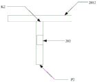
Referring to fig. 1-2, fig. 1-2 is a schematic diagram illustrating the connection between the second feeding connection point K2 and the second feeding point P2, and as shown in fig. 1-2, the second feeding connection point K2 may be connected to the second feeding point P2 through the lumped inductor 202. In addition, in the embodiment of the present invention, a first capacitor partition G1 and a second capacitor partition G2 may be respectively disposed between the second feeding connection point K2 and the one end Q2 of the second metal bezel 201, and between the second feeding connection point K2 and the other end Q1 of the second metal bezel 201, fig. 1 to 3 are enlarged top views of adjacent portions of the second left bezel 2011 and the second middle bezel 2012, as shown in fig. 1 to 3, the second left bezel 2011 and the second middle bezel 2012 are not connected, a gap exists between the second left bezel 2011 and the second middle bezel 2012, the gap is the above-mentioned first capacitor partition G1, fig. 1 to 4 are enlarged top views of adjacent portions of the second right bezel 2013 and the second middle bezel 2012, as shown in fig. 1 to 4, the second right bezel 2013 and the second middle bezel 2012 are not connected, and a gap exists between the second right bezel 2013 and the second middle bezel 2012, this gap is the second capacitive partition G2.
The first capacitor partition G1 and the second capacitor partition G2 disposed on the second metal frame 201 are equivalent to disposing capacitors on two radiation segments of the second antenna, and the lumped inductor 202 disposed between the second feeding connection point K2 and the second feeding point P2 is equivalent to disposing inductors on two radiation segments of the second antenna. The arrangement of the capacitor and the inductor can reduce the frequency point of the fundamental mode resonance generated by the two radiation sections, thereby reducing the size required by the two radiation sections.
In addition, in order to enable the antenna array to operate in different frequency bands, that is, to enable the first antenna and the second antenna to generate fundamental mode resonance at different frequency points, in the embodiments of the present invention, the sizes of the radiation sections of the first antenna and the second antenna may be changed by using a reconfigurable technology.
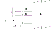
Referring to fig. 1-5, fig. 1-5 are enlarged schematic views of an end L2 of the first metal bezel 101, as shown in fig. 1-5, an end L2 of the first metal bezel 101 may be connected to the ground plane D through a first ground switch H1, and a first reconfiguration switch group F1 is disposed adjacent to the end L2 of the first metal bezel 101, the first reconfiguration switch group F1 includes at least one first reconfiguration switch F1 (fig. 1-5 only show that the first reconfiguration switch group F1 includes two first reconfiguration switches F1), and each first reconfiguration switch F1 is respectively connected to the first metal bezel 101 and the ground plane D. In practical applications, the other end L1 of the first metal frame 101 may also be provided with a first grounding switch H1 and a first reconfiguration switch group F1 similarly to the one end L2 of the first metal frame 101, which is not described again in this embodiment of the present invention.
The position of the connection of the first metal bezel 101 to the ground plane D can be changed by controlling the closing and opening of the first grounding switch H1 and each of the first reconfiguration switches f1, thereby changing the size of the first antenna radiation segment.
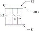
Referring to fig. 1-6, fig. 1-6 are enlarged schematic views of an end Q1 of the second metal frame 201, as shown in fig. 1-6, the end Q1 of the second metal frame 201 is connected to the ground plate D through a second ground switch H2, and a second reconfiguration switch group F2 is disposed adjacent to the end Q1 of the second metal frame 201, the second reconfiguration switch group F2 includes at least one second reconfiguration switch F2 (fig. 1-6 only show that the second reconfiguration switch group F2 includes two second reconfiguration switches F2), and each second reconfiguration switch F2 is respectively connected to the second metal frame 201 and the ground plate D. In practical applications, the other end Q2 of the second metal frame 201 may also be provided with a second grounding switch H2 and a second reconfiguration switch group F2 similarly to the one end Q1 of the second metal frame 201, which is not described again in the embodiment of the present invention.
Likewise, the position of the connection of the second metal bezel 201 to the ground plane D can be changed by controlling the closing and opening of the second ground switch H2 and each second reconfiguration switch f2, thereby changing the size of the second antenna radiation section.
It should be noted that, in practical applications, the closing and opening of the first grounding switch H1, each of the first reconfiguration switches f1, the second grounding switch H2, and each of the second reconfiguration switches f2 may be controlled by a processor in the terminal, and the embodiment of the present invention is not described herein again.
In the following, the embodiments of the present invention only describe the sizes of the first antenna and the second antenna with the antenna array operating in the LTE700 frequency band and the GSM850/900 frequency band, and it should be noted that the following description of the size of the antenna array is only exemplary and is not intended to limit the present application.
When the antenna array operates on the LTE700 frequency band, the length d1 of the first right side frame 1013 is 70 mm, the length d2 of the first middle frame 1012 is 70 mm, the distance d3 from the first feed connection point K1 to the first middle frame 1012 is 61 mm, and the distance d4 from the first feed connection point K1 to one end L1 of the first metal frame 101 is 61 mm. The gap width r1 between the first middle rim 1012 and the ground plate D is 12 mm, the gap width r2 between the first right rim 1013 and the ground plate D is 2 mm, and the gap width r3 between the first left rim 1011 and the ground plate D is 2 mm. The length s1 of the second left side frame 2011 is 77 mm, the length s2 of the second right side frame 2013 is 72 mm, the distance s3 from the second left side frame 2011 to the second feed connection point K2 is 31 mm, the distance s4 from the second feed connection point K2 to the second right side frame 2013 is 39 mm, the widths of the first capacitor partition G1 and the second capacitor partition G2 are 0.2 mm, the size of the lumped inductor 202 is 4.7 nanohenries, and the distance h from the second metal frame 201 to the ground plate D is 7 mm.
When the antenna array operates in the GSM850/900 band, the length d1 of the first right side frame 1013 is 58 mm, the length d2 of the first middle frame 1012 is 70 mm, the distance d3 from the first feed connection point K1 to the first middle frame 1012 is 41 mm, and the distance d4 from the first feed connection point K1 to the end L1 of the first metal frame 101 is 21 mm. The gap width r1 between the first middle rim 1012 and the ground plate D is 12 mm, the gap width r2 between the first right rim 1013 and the ground plate D is 2 mm, and the gap width r3 between the first left rim 1011 and the ground plate D is 2 mm. The length s1 of the second left side frame 2011 is 57 mm, the length s2 of the second right side frame 2013 is 62 mm, the distance s3 from the second left side frame 2011 to the second feed connection point K2 is 31 mm, the distance s4 from the second feed connection point K2 to the second right side frame 2013 is 39 mm, the widths of the first capacitor partition G1 and the second capacitor partition G2 are 0.2 mm, the size of the lumped inductor 202 is 2.1 nanohenry, and the distance h from the second metal frame 201 to the ground plate D is 7 mm.
Fig. 2 is a schematic diagram illustrating return loss of a first antenna when only the first antenna is disposed in a terminal and the first antenna operates in an LTE700 frequency band, where an x-axis in fig. 2 represents an electromagnetic frequency, and a unit is GHz, and a y-axis represents a port S parameter, and a unit is db. As can be seen from fig. 2, the first antenna can generate fundamental mode resonance at a frequency point of 760MHz, and can better cover various frequency points included in the LTE700 frequency band.
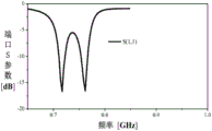
Fig. 3 is a schematic diagram illustrating a return loss of a second antenna when only the second antenna is disposed in a terminal and the second antenna operates in an LTE700 frequency band, where an x-axis in fig. 3 represents an electromagnetic frequency, and a unit is GHz, and a y-axis represents a port S parameter, and a unit is db. As can be seen from fig. 3, the second antenna can generate fundamental mode resonances at frequency points of 720MHz and 760MHz, and can better cover various frequency points included in the LTE700 frequency band.
Fig. 4 is a schematic diagram showing return loss of a first antenna when only the first antenna is disposed in a terminal and the first antenna operates in a GSM850/900 frequency band, where an x-axis in fig. 4 represents an electromagnetic wave frequency in GHz, and a y-axis represents a port S parameter in db. As can be seen from fig. 4, the first antenna can generate fundamental mode resonance at the frequency point of 900MHz, and can better cover various frequency points included in the GSM850/900 frequency band.
Fig. 5 is a schematic diagram showing return loss of a second antenna when only the second antenna is disposed in the terminal and the second antenna operates in the GSM850/900 frequency band, where in fig. 5, the x-axis represents electromagnetic wave frequency in GHz, and the y-axis represents port S parameter in db. As can be seen from FIG. 5, the second antenna can generate fundamental mode resonance at 870MHz and 950MHz frequency points, and can better cover various frequency points included in the GSM850/900 frequency band.
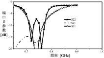
Fig. 6 is a schematic diagram showing return loss and isolation of a first antenna and a second antenna when the terminal is provided with the first antenna and the second antenna, and both the first antenna and the second antenna operate in an LTE700 frequency band, where an x-axis in fig. 6 represents an electromagnetic frequency, and a unit is GHz, and a y-axis represents a port S parameter, and a unit is db. As can be seen from fig. 6, the second antenna can generate fundamental mode resonance at the frequency points of 720MHz and 760MHz, and can better cover each frequency point included in the LTE700 frequency band, the first antenna can generate fundamental mode resonance at the frequency point of 740MHz, and can better cover each frequency point included in the LTE700 frequency band, the return loss curves of the first antenna and the second antenna are substantially the same as the return loss curves of the first antenna and the second antenna when one first antenna or one second antenna is separately disposed in the terminal, and the isolation between the first antenna and the second antenna is less than 15db, and the isolation is better.
Fig. 7 is a schematic diagram showing return loss and isolation of a first antenna and a second antenna when the first antenna and the second antenna are both operated in a GSM850/900 frequency band, where in fig. 7, an x axis represents electromagnetic wave frequency, and a unit is GHz, and a y axis represents a port S parameter, and a unit is db. As can be seen from fig. 7, the second antenna can generate fundamental mode resonance at the frequency points of 850MHz and 950MHz, and can better cover each frequency point included in the GSM850/900 frequency band, the first antenna can generate fundamental mode resonance at the frequency point of 900MHz, and can better cover each frequency point included in the GSM850/900 frequency band, the return loss curves of the first antenna and the second antenna are substantially the same as the return loss curves of the first antenna and the second antenna when one first antenna or one second antenna is separately disposed in the terminal, and the isolation between the first antenna and the second antenna is less than 15db, and the isolation is better.
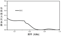
Fig. 8 is a schematic diagram illustrating an Envelope Correlation Coefficient (ECC) of an antenna array when the antenna array operates in an LTE700 frequency band according to an embodiment of the present invention, where an x-axis in fig. 8 represents an electromagnetic frequency, a unit is GHz, and a y-axis represents an ECC value. As shown in fig. 8, the ECC value of the antenna array is small, and therefore the envelope correlation of the first antenna and the second antenna in the antenna array is low.
Fig. 9 is a schematic diagram illustrating an ECC of an antenna array according to an embodiment of the present invention when the antenna array operates in a GSM850/900 frequency band, where an x-axis in fig. 9 represents an electromagnetic frequency, a unit is GHz, and a y-axis represents an ECC value, as shown in fig. 9, the ECC value of the antenna array is smaller, and therefore, the envelope correlation between a first antenna and a second antenna in the antenna array is lower.
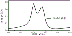
Fig. 10 is a schematic diagram illustrating the total efficiency of the first antenna when operating in the GSM850/900 frequency band, where the x-axis in fig. 10 represents the frequency of the electromagnetic wave, the unit is GHz, and the y-axis represents the value of the total efficiency, as shown in fig. 10, the total efficiency of the first antenna can reach more than 50%, and the efficiency is high.
Fig. 11 is a schematic diagram illustrating the total efficiency of the second antenna when operating in the GSM850/900 frequency band, where the x-axis in fig. 11 represents the frequency of the electromagnetic wave, the unit is GHz, and the y-axis represents the value of the total efficiency, as shown in fig. 11, the total efficiency of the second antenna can reach more than 35%.
Fig. 12 is a schematic diagram illustrating the total efficiency of the first antenna when operating in the LTE700 band, where the x-axis in fig. 12 represents the frequency of the electromagnetic wave, the unit is GHz, and the y-axis represents the value of the total efficiency, as shown in fig. 12, the total efficiency of the first antenna can reach more than 50%, and the efficiency is high.
Fig. 13 is a schematic diagram illustrating the total efficiency of the second antenna when operating in the LTE700 band, where the x-axis in fig. 13 represents the frequency of the electromagnetic wave, the unit is GHz, and the y-axis represents the value of the total efficiency, as shown in fig. 13, the total efficiency of the second antenna can reach more than 35%.
In summary, in the antenna array provided in the embodiment of the present invention, the first metal frame serving as the first antenna radiator is disposed to be coplanar with the ground plane, and the second metal frame serving as the second antenna radiator is disposed to be not coplanar with the ground plane and parallel to the ground plane, so that the polarization directions of the first antenna and the second antenna are orthogonal, and thus the influence between the electromagnetic waves radiated by the first antenna and the second antenna is smaller, that is, the coupling between the first antenna and the second antenna is smaller.
The embodiment of the invention also provides a terminal, wherein the terminal is provided with the antenna array shown in fig. 1-1, and the terminal can use the antenna array to receive and transmit communication information.
It should be noted that the terminal provided in the embodiment of the present invention may be an electronic device capable of sending and receiving communication information, such as a mobile phone, a tablet computer, and the like. Embodiments of the present invention provide a terminal that may include a processing component, a memory, a power component, a multimedia component, an audio component, an input/output interface, a sensor component, and a communication component.
Wherein the processing component is used to control overall operation of the terminal, such as operations associated with display, telephone calls, data communications, camera operations and recording operations. In one embodiment of the invention, the processing component may include one or more processors.
The memory is configured to store various types of data to support operation of the terminal. Examples of such data include instructions for any application or method operating on the terminal, contact data, phonebook data, messages, pictures, videos, etc. The memory may be implemented by any type or combination of volatile or non-volatile storage devices, such as static random access memory, electrically erasable programmable read only memory, magnetic memory, flash memory, magnetic or optical disks, or the like.
The power supply component may provide power to various components of the terminal.
The multimedia component includes a screen providing an output interface between the terminal and the user. In some embodiments of the present invention, the screen may include a liquid crystal display and a touch panel. In some embodiments of the present invention, the multimedia component may further comprise a front-facing camera and/or a rear-facing camera.
The audio component is configured to output and/or input an audio signal. For example, the audio component may include a microphone and, in some embodiments of the invention, the audio component may also include a speaker.
The input/output interface provides an interface between the processing component and a peripheral interface module, which may be a keyboard, click wheel, buttons, etc.
The sensor assembly includes one or more sensors for providing various aspects of status assessment to the terminal. In one embodiment of the invention, the sensor assembly may include a proximity sensor, a light sensor, an acceleration sensor, a gyroscope sensor, a magnetic sensor, a pressure sensor or a temperature sensor, or the like.
The communication component is configured to facilitate wired or wireless communication between the terminal and other devices. In one exemplary embodiment of the present invention, the communication part may include a near field communication module or the like.
The above description is only exemplary of the present application and should not be taken as limiting the present application, and any modifications, equivalents, improvements and the like that are made within the spirit and principle of the present application should be included in the protection scope of the present application.