CN109313402B - Alignment System Wafer Stacking Beam Profiler - Google Patents
Alignment System Wafer Stacking Beam Profiler Download PDFInfo
- Publication number
- CN109313402B CN109313402B CN201780034179.4A CN201780034179A CN109313402B CN 109313402 B CN109313402 B CN 109313402B CN 201780034179 A CN201780034179 A CN 201780034179A CN 109313402 B CN109313402 B CN 109313402B
- Authority
- CN
- China
- Prior art keywords
- substrate
- alignment system
- overlay
- targets
- light
- Prior art date
- Legal status (The legal status is an assumption and is not a legal conclusion. Google has not performed a legal analysis and makes no representation as to the accuracy of the status listed.)
- Active
Links
Images


Classifications
-
- G—PHYSICS
- G03—PHOTOGRAPHY; CINEMATOGRAPHY; ANALOGOUS TECHNIQUES USING WAVES OTHER THAN OPTICAL WAVES; ELECTROGRAPHY; HOLOGRAPHY
- G03F—PHOTOMECHANICAL PRODUCTION OF TEXTURED OR PATTERNED SURFACES, e.g. FOR PRINTING, FOR PROCESSING OF SEMICONDUCTOR DEVICES; MATERIALS THEREFOR; ORIGINALS THEREFOR; APPARATUS SPECIALLY ADAPTED THEREFOR
- G03F9/00—Registration or positioning of originals, masks, frames, photographic sheets or textured or patterned surfaces, e.g. automatically
- G03F9/70—Registration or positioning of originals, masks, frames, photographic sheets or textured or patterned surfaces, e.g. automatically for microlithography
- G03F9/7049—Technique, e.g. interferometric
-
- G—PHYSICS
- G03—PHOTOGRAPHY; CINEMATOGRAPHY; ANALOGOUS TECHNIQUES USING WAVES OTHER THAN OPTICAL WAVES; ELECTROGRAPHY; HOLOGRAPHY
- G03F—PHOTOMECHANICAL PRODUCTION OF TEXTURED OR PATTERNED SURFACES, e.g. FOR PRINTING, FOR PROCESSING OF SEMICONDUCTOR DEVICES; MATERIALS THEREFOR; ORIGINALS THEREFOR; APPARATUS SPECIALLY ADAPTED THEREFOR
- G03F9/00—Registration or positioning of originals, masks, frames, photographic sheets or textured or patterned surfaces, e.g. automatically
- G03F9/70—Registration or positioning of originals, masks, frames, photographic sheets or textured or patterned surfaces, e.g. automatically for microlithography
- G03F9/7073—Alignment marks and their environment
-
- G—PHYSICS
- G03—PHOTOGRAPHY; CINEMATOGRAPHY; ANALOGOUS TECHNIQUES USING WAVES OTHER THAN OPTICAL WAVES; ELECTROGRAPHY; HOLOGRAPHY
- G03F—PHOTOMECHANICAL PRODUCTION OF TEXTURED OR PATTERNED SURFACES, e.g. FOR PRINTING, FOR PROCESSING OF SEMICONDUCTOR DEVICES; MATERIALS THEREFOR; ORIGINALS THEREFOR; APPARATUS SPECIALLY ADAPTED THEREFOR
- G03F9/00—Registration or positioning of originals, masks, frames, photographic sheets or textured or patterned surfaces, e.g. automatically
- G03F9/70—Registration or positioning of originals, masks, frames, photographic sheets or textured or patterned surfaces, e.g. automatically for microlithography
- G03F9/7088—Alignment mark detection, e.g. TTR, TTL, off-axis detection, array detector, video detection
Landscapes
- Physics & Mathematics (AREA)
- General Physics & Mathematics (AREA)
- Engineering & Computer Science (AREA)
- Multimedia (AREA)
- Exposure And Positioning Against Photoresist Photosensitive Materials (AREA)
- Length Measuring Devices By Optical Means (AREA)
- Container, Conveyance, Adherence, Positioning, Of Wafer (AREA)
Abstract
一种对准系统获得从晶片堆叠返回的光的特性。光束分析器测量波长、偏振和光束轮廓的变化。该测得信息允许在线工艺变化校正。校正提供单个标记堆叠变化的光学监控,并接着提供信息以减小单个标记工艺变化诱发的精确性误差。
An alignment system acquires the properties of light returning from a wafer stack. A beam analyzer measures variations in wavelength, polarization, and beam profile. This measured information allows for in-line correction of process variations. The correction provides optical monitoring of individual marker stack variations and subsequently provides information to reduce accuracy errors induced by individual marker process variations.
Description
相关申请的交叉引用CROSS-REFERENCE TO RELATED APPLICATIONS
本申请要求享有于2016年6月3日提交的美国临时专利申请No.62/345,678的优先权,并且该申请在此通过全文引用的方式并入本文。This application claims priority to US Provisional Patent Application No. 62/345,678, filed June 3, 2016, and incorporated herein by reference in its entirety.
技术领域technical field
本公开涉及一种对准系统,其例如可以用于光刻设备中。The present disclosure relates to an alignment system, which may be used, for example, in a lithographic apparatus.
背景技术Background technique
光刻设备是将所需图案施加至衬底的目标部分上的机器。光刻设备可以用于例如集成电路(IC)的制造中。在该情形中,备选地称作掩模或刻线板的图案化装置可以用于产生与IC的单个层相对应的电路图案,并且可以将该图案成像至具有辐射敏感层(抗蚀剂)的衬底(例如硅晶片)上的目标部分(例如包括一个或数个管芯的一部分)上。一般地,单个衬底将包含后续曝光的相邻目标部分的网络。已知的光刻设备包括所谓的步进机,其中通过将整个图案一次性曝光至目标部分上而照射每个目标部分,以及所谓的扫描机,其中通过沿给定方向(“扫描”方向)扫描图案穿过光束而同时同步地平行于或反平行于该方向扫描衬底而照射每个目标部分。也可能通过将图案压印至衬底上而将图案从图案化装置转移至衬底。另一光刻系统是干涉仪光刻系统,其中没有图案化装置,而是相反地光束被分割成两个光束,以及通过使用反射系统使得两个光束在衬底的目标部分处相干。相干使得在衬底的目标部分上形成线条。A lithographic apparatus is a machine that applies a desired pattern to a target portion of a substrate. Lithographic apparatuses can be used, for example, in the manufacture of integrated circuits (ICs). In this case, a patterning device, alternatively referred to as a mask or reticle, can be used to create a circuit pattern corresponding to a single layer of the IC, and this pattern can be imaged to have a radiation-sensitive layer (resist ) on a target portion (eg, a portion comprising one or more dies) on a substrate (eg, a silicon wafer). Typically, a single substrate will contain a network of adjacent target portions for subsequent exposures. Known lithographic apparatuses include so-called steppers, in which each target portion is irradiated by exposing the entire pattern onto the target portion at once, and so-called scanners, in which the target portion is irradiated by exposing it in a given direction (the "scanning" direction) The scanning pattern passes through the beam while simultaneously scanning the substrate parallel or antiparallel to the direction to illuminate each target portion. It is also possible to transfer the pattern from the patterning device to the substrate by imprinting the pattern onto the substrate. Another lithography system is an interferometer lithography system, in which there is no patterning device, but instead the beam is split into two beams, and the two beams are made coherent at the target portion of the substrate by using a reflection system. Coherence causes lines to form on the target portion of the substrate.
在光刻操作期间,不同的处理步骤可以要求在衬底上顺序地形成不同层。因此,可以需要相对于形成在其上的现有的图案而以高精确度定位衬底。一般地,对准标记放置在待对准的衬底上并且定位参照第二目标。光刻设备可以使用对准系统以用于检测对准标记的位置并使用对准标记对准衬底以确保从掩模精确曝光。在两个不同层处对准标记之间未对准测量作为套刻误差。During a lithographic operation, different processing steps may require the sequential formation of different layers on the substrate. Therefore, it may be necessary to position the substrate with high accuracy relative to the existing pattern formed thereon. Typically, alignment marks are placed on the substrate to be aligned and positioned with reference to a second target. A lithographic apparatus can use an alignment system for detecting the location of alignment marks and aligning the substrate using the alignment marks to ensure accurate exposure from the mask. Misalignment between alignment marks at two different layers is measured as overlay error.
理想地,套刻误差仅仅是在光刻系统内衬底定位的产物。然而实际上,套刻误差源自对准系统与衬底之间的相互作用。对准系统和衬底中变化可以在评估对准标记的真实位置中产生误差。该误差已知为“工艺上”精确性误差。对准系统光学元件包含制造像差,并且因此无法等同。同样,衬底(例如晶片堆叠)具有源自制造和后制造工艺的特性变化。该“工艺上”精确性问题限制了对准系统的健壮性。Ideally, overlay errors are simply the product of substrate positioning within the lithography system. In practice, however, overlay errors arise from the interaction between the alignment system and the substrate. Variations in the alignment system and substrate can create errors in evaluating the true position of the alignment marks. This error is known as an "craftsman" accuracy error. Alignment system optics contain manufacturing aberrations and are therefore not equivalent. Likewise, substrates (eg, wafer stacks) have characteristic variations derived from fabrication and post-fabrication processes. This "in-process" accuracy problem limits the robustness of the alignment system.
因此,需要补偿对准系统中变化和衬底中工艺变化。Therefore, there is a need to compensate for variations in the alignment system and process variations in the substrate.
发明内容SUMMARY OF THE INVENTION
根据一个实施例,一种对准系统包括产生光的辐射源、光学调制单元、光学分束器、干涉仪、一个或多个检测器、光束分析器以及处理器。According to one embodiment, an alignment system includes a radiation source that produces light, an optical modulation unit, an optical beam splitter, an interferometer, one or more detectors, a beam analyzer, and a processor.
在一个实施例中,将由辐射源产生的光引导朝向衬底。光学分束器将从衬底上图案衍射、或从衬底反射的光束分裂成子光束。干涉仪干涉至少一个子光束并根据干涉产生输出光。一个或多个检测器从干涉仪接收输出光,并且确定衬底的对准状态。光束分析器从光学分束器接收已经从衬底上图案衍射或从衬底反射的至少一个子光束,并且提供图案的套刻误差测量或者光束分布的光学状态。光束分析器也可以基于光束分布而确定产品堆叠分布。处理器利用相关性算法以基于从一个或多个检测器和光束分析器接收的信息而确定套刻偏移误差,以及使用所确定的套刻偏移误差和产品堆叠分布产生校正表。处理器使用校正表以确定对于每个掩模的校正,并将校正返回馈送至对准系统以用于校正套刻偏移中的误差。处理器可以重复对于每个标记的以上过程,并且可以产生自我学习反馈回路以用于改善衬底的对准状态。处理器随后可以引导对准系统在更新的位置放置衬底以用于改进对准精确性。In one embodiment, the light generated by the radiation source is directed towards the substrate. The optical beam splitter splits the beam diffracted from the pattern on the substrate, or reflected from the substrate, into sub-beams. The interferometer interferes with the at least one sub-beam and produces output light based on the interference. One or more detectors receive the output light from the interferometer and determine the alignment state of the substrate. The beam analyzer receives from the optical beam splitter at least one sub-beam that has been diffracted from the pattern on the substrate or reflected from the substrate, and provides an overlay error measure of the pattern or an optical state of the beam profile. The beam profiler can also determine the product stack distribution based on the beam distribution. The processor utilizes a correlation algorithm to determine the overlay offset error based on information received from the one or more detectors and the beam analyzer, and generates a correction table using the determined overlay offset error and product stack distribution. The processor uses the correction table to determine the correction for each mask and feeds the correction back to the alignment system for use in correcting errors in the overlay offset. The processor can repeat the above process for each mark, and can generate a self-learning feedback loop for improving the alignment state of the substrate. The processor may then direct the alignment system to place the substrate at the updated location for improved alignment accuracy.
以下参照附图详细描述本发明的其他特征和优点、以及本发明各个实施例的结构和操作。应该注意,本发明不限于在此所述的具体实施例。在此仅为了示意说明目的展示这些实施例。基于在此所包含的教导,额外的实施例对于本领域技术人员将是明显的。Other features and advantages of the present invention, as well as the structure and operation of various embodiments of the present invention, are described in detail below with reference to the accompanying drawings. It should be noted that the present invention is not limited to the specific embodiments described herein. These embodiments are shown here for illustrative purposes only. Additional embodiments will be apparent to those skilled in the art based on the teachings contained herein.
附图说明Description of drawings
在此所包含并形成了说明书的一部分的附图说明了本发明,并且与说明书一起进一步用于解释本发明的原理以及使得本领域技术人员制造和使用本发明。The accompanying drawings incorporated herein and forming a part of the specification illustrate the invention and, together with the description, further serve to explain the principles of the invention and to enable those skilled in the art to make and use the invention.
图1A是根据一个实施例的反射式光刻设备的示意图。Figure 1A is a schematic diagram of a reflective lithographic apparatus according to one embodiment.
图1B是根据一个实施例的透射式光刻设备的示意图。Figure IB is a schematic diagram of a transmissive lithographic apparatus according to one embodiment.
图2是根据一个实施例的反射式光刻设备的更详细示意图。Figure 2 is a more detailed schematic diagram of a reflective lithographic apparatus according to one embodiment.
图3是根据一个实施例的光刻单元的示意图。3 is a schematic diagram of a lithography cell according to one embodiment.
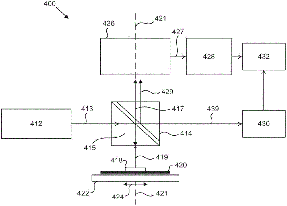
图4A和图4B是根据各种实施例的增强对准系统的示意图。4A and 4B are schematic diagrams of enhanced alignment systems according to various embodiments.
图5是可以用在根据一个实施例的设备中的计算机系统。Figure 5 is a computer system that may be used in an apparatus according to one embodiment.
图6是用于使用根据各个实施例的增强对准系统并使用信息以提供更精确对准的检查晶片的方法的流程图。6 is a flowchart of a method for inspecting a wafer using an enhanced alignment system and using information to provide more precise alignment in accordance with various embodiments.
当结合附图时本发明的特征和优点将从以下所阐述的详细说明书变得更明显,其中遍及全部相同的参考符号标识对应的元件。在附图中,相同的参考数字通常指示等同、功能类似、和/或结构类似的元件。其中元件首次出现的附图由对应参考数字中最左侧数位指示。除非另外指示,遍及本公开所提供的附图不应解释为按照比例绘制。The features and advantages of the present invention will become more apparent from the detailed description set forth below when taken in conjunction with the accompanying drawings, wherein like reference characters identify corresponding elements throughout. In the drawings, like reference numerals generally designate equivalent, functionally similar, and/or structurally similar elements. The drawing in which an element first appears is indicated by the leftmost digit in the corresponding reference number. Unless otherwise indicated, the drawings provided throughout this disclosure should not be construed as being drawn to scale.
具体实施方式Detailed ways
本说明书公开了包括本发明特征的一个或多个实施例。所公开的实施例仅仅示例化了本发明。本发明的范围不限于所公开的实施例。本发明由所附权利要求限定。This specification discloses one or more embodiments that incorporate the features of the invention. The disclosed embodiments merely illustrate the invention. The scope of the present invention is not limited to the disclosed embodiments. The invention is defined by the appended claims.
在说明书中描述为并参考“一个实施例”、“一实施例”、“示例性实施例”等的实施例指示了所述实施例可以包括特定的特征、结构或特性,但是并非每个实施例必须包括该特定特征、结构或特性。此外,该短语不必涉及相同的实施例。进一步,当结合实施例描述特定特征、结构或特性时,应该理解,不论是否明确描述,结合其他实施例而实现该特征、结构或特性在本领域技术人员的知识范围内。Embodiments described in the specification as "one embodiment," "an embodiment," "exemplary embodiment," etc., indicate that the embodiment may include a particular feature, structure, or characteristic, but not every implementation. The instance must include that particular feature, structure or characteristic. Furthermore, the phrases do not necessarily refer to the same embodiment. Further, when a particular feature, structure or characteristic is described in conjunction with one embodiment, it should be understood that it is within the knowledge of those skilled in the art to implement that feature, structure or characteristic in conjunction with other embodiments, whether explicitly described or not.
然而,在更详细描述这些实施例之前,展示其中可以实施本发明实施例的示例性环境是有益的。Before describing these embodiments in greater detail, however, it is beneficial to show an exemplary environment in which embodiments of the invention may be implemented.
反射式和透射式光刻系统的示例Examples of Reflective and Transmissive Lithography Systems
图1A和图1B分别是其中可以实施本发明的一个实施例的光刻设备100和光刻设备100’的示意图。光刻设备100和光刻设备100’均包括以下项:照射系统(照射器)IL,被配置用于调节辐射束B(例如深紫外或极紫外辐射);支撑结构(例如掩模工作台)MT,被配置用于支撑图案化装置(例如掩模、刻线板或动态图案化装置)MA并连接至被配置用于精确地定位图案化装置MA的第一定位器PM;以及衬底工作台(例如晶片工作台)WT,被配置用于固定衬底(例如涂覆了抗蚀剂的晶片)W并连接至配置用于精确地定位衬底W的第二定位器PW。光刻设备100和100’也具有投影系统PS,被配置用于将由图案化装置MA赋予辐射束B的图案投影至衬底W的目标部分(例如包括一个或多个管芯)C上。在光刻设备100中,图案化装置MA和投影系统PS是反射式的。在光刻设备100’中,图案化装置MA和投影系统PS是透射式的。Figures 1A and 1B are schematic diagrams, respectively, of a
照射系统IL可以包括用于引导、定形、或控制辐射束B的各种类型光学部件,诸如折射式、反射式、折反射式、磁性、电磁、静电、或其他类型光学部件、或其任意组合。The illumination system IL may include various types of optical components for directing, shaping, or steering the radiation beam B, such as refractive, reflective, catadioptric, magnetic, electromagnetic, electrostatic, or other types of optical components, or any combination thereof .
支撑结构MT以取决于图像化装置MA相对于参考框架的定向、光刻设备100和100’的至少一个的设计、以及诸如图案化装置MA是否固定在真空环境中的方式之类的其他条件而固定图案化装置MA。支撑结构MT可以使用机械、真空、静电或其他夹持技术以固定图案化装置MA。支撑结构MT可以是框架或工作台,例如,如需要的话,其可以是固定或可移动的。通过使用传感器,支撑结构MT可以确保图案化装置MA处于所需位置处,例如,相对于投影系统PS。The support structure MT depends on the orientation of the imaging device MA relative to the reference frame, the design of at least one of the
术语“图案化装置”MA应该广义地解释为涉及可以用于在其截面中赋予辐射束B图案以便于在衬底W的目标部分C中产生图案的任何装置。赋予辐射束B的图案可以对应于在目标部分C中所形成的器件中的特定功能层以形成集成电路。The term "patterning device" MA should be interpreted broadly to refer to any device that can be used to impart a pattern to the radiation beam B in its cross-section so as to create a pattern in the target portion C of the substrate W. The pattern imparted to the radiation beam B may correspond to specific functional layers in the device formed in the target portion C to form an integrated circuit.
图案化装置MA可以是透射式(如图1B的光刻设备100’中)或反射式(如图1A的光刻设备100中)。图案化装置MA的示例包括刻线板、掩模、可编程镜面阵列、以及可编程LCD面板。掩模在光刻中广泛已知,并且包括诸如二元、交替相移、和衰减相移的掩模类型,以及各种混合掩模类型。可编程镜面阵列的示例采用小镜面的矩阵布置,每个小镜面可以单独地倾斜以便于沿不同方向反射入射的辐射束。倾斜的镜面在由小镜面的阵列所反射的辐射束B中赋予图案。The patterning device MA may be transmissive (as in the lithographic apparatus 100' of FIG. IB) or reflective (as in the
术语“投影系统”PS可以包括任何类型投影系统,包括折射、反射、折反射、磁性、电磁或经典光学系统、或其任意组合,如对于所使用曝光辐射合适的,或者对于其他因素诸如在衬底W上使用沉浸液体或者使用真空合适的。真空环境可以用于EUV或电子束辐射,因为其他气体可以吸收太多辐射或电子。可以因此借助于真空壁和真空泵而向整个光束路径提供真空环境。The term "projection system" PS may include any type of projection system, including refractive, reflective, catadioptric, magnetic, electromagnetic or classical optical systems, or any combination thereof, as appropriate for the exposure radiation used, or for other factors such as the Use an immersion liquid on the bottom or use a vacuum as appropriate. A vacuum environment can be used for EUV or electron beam radiation because other gases can absorb too much radiation or electrons. The entire beam path can thus be provided with a vacuum environment by means of a vacuum wall and a vacuum pump.
光刻设备100和/或光刻设备100’可以是具有两个(双平台)或更多衬底工作台WT(和/或两个或更多掩模工作台)的类型。在该“多平台”机器中,额外的衬底工作台WT可以并行使用,或者可以在一个或多个工作台上执行预备步骤而同时一个或多个其他衬底工作台用于曝光。在一些情形中,额外的工作台可以不是衬底工作台WT。The
参照图1A和图1B,照射器IL从辐射源SO接收辐射束。源SO和光刻设备100、100’可以是分离的物理实体,例如,当源SO是受激准分子激光器时。在该情形中,源SO不应视作形成了光刻设备100或100’的一部分,并且辐射束B借助于包括例如合适的引导镜面和/或扩束器的光束输送系统BD(在图1B中)而从源SO传至照射器IL。在其他情形中,源SO可以是光刻设备100、100’的整体部分-例如当源SO是汞灯时。源SO和照射器IL以及如果需要的话与光束输送系统BD一起可以称作辐射系统。1A and 1B, the illuminator IL receives a radiation beam from a radiation source SO. The source SO and the
照射器IL可以包括调节器AD(在图1B中)用于调节辐射束的角强度分布。一般地,可以调节在照射器的光瞳面中强度分布的至少外侧和/或内侧径向范围(通常分别称作“σ-外侧”和“σ-内侧”)。此外,照射器IL可以包括各种其他部件(在图1B中),诸如积分器IN和聚光器CO。照射器IL可以用于调节辐射束B以在其截面中具有所需均匀性和强度分布。The illuminator IL may include an adjuster AD (in Figure IB) for adjusting the angular intensity distribution of the radiation beam. Generally, at least the outer and/or inner radial extent (commonly referred to as "σ-outer" and "σ-inner", respectively) of the intensity distribution in the pupil plane of the illuminator can be adjusted. In addition, the illuminator IL may include various other components (in FIG. 1B ), such as the integrator IN and the concentrator CO. The illuminator IL can be used to condition the radiation beam B to have the desired uniformity and intensity distribution in its cross section.
参照图1A,辐射束B入射在图案化装置(例如掩模)MA上,其被固定在支撑结构(例如掩模工作台)MT上,并由图案化装置MA图案化。在光刻设备100中,辐射束B从图案化装置(例如掩模)MA反射。在从图案化装置(例如掩模)MA反射之后,辐射束B穿过投影系统PS,其将辐射束B聚焦至衬底W的目标部分C上。借助于第二定位器PW和位置传感器IF2(例如干涉仪装置、线性编码器或电容性传感器),衬底工作台WT可以精确地移动(例如以便于在辐射束B的路径中定位不同目标部分C)。类似地,第一定位器PM和另一位置传感器IF1可以用于相对于辐射束B的路径精确地定位图案化装置(例如掩模)MA。可以使用掩模对准标记M1、M2以及衬底对准标记P1、P2对准图案化装置(例如掩模)MA和衬底W。1A, a radiation beam B is incident on a patterning device (eg, a mask) MA, which is fixed on a support structure (eg, a mask table) MT, and is patterned by the patterning device MA. In the
参照图1B,辐射束B入射在图案化装置(例如掩模MA)上,其被固定在支撑结构(例如掩模工作台MT)上,并由图案化装置图案化。已经横越了掩模MA,辐射束B穿过投影系统PS,其将光束聚焦至衬底W的目标部分C上。投影系统具有与照射系统光瞳IPU共轭的光瞳PPU。辐射的一部分从在照射系统光瞳IPU处强度分布发源并横越掩模图案而并未受到在掩模图案处衍射的影响,并且在照射系统光瞳IPU处产生强度分布的图像。Referring to Figure IB, a radiation beam B is incident on a patterning device (eg, mask MA), which is fixed on a support structure (eg, mask table MT), and is patterned by the patterning device. Having traversed the mask MA, the radiation beam B passes through the projection system PS, which focuses the beam onto the target portion C of the substrate W. The projection system has a pupil PPU that is conjugate to the illumination system pupil IPU. A portion of the radiation originates from the intensity distribution at the illumination system pupil IPU and traverses the mask pattern unaffected by diffraction at the mask pattern and produces an image of the intensity distribution at the illumination system pupil IPU.
借助于第二定位器PW和位置传感器IF(例如干涉仪装置、线性编码器、或电容性传感器),可以精确地移动衬底工作台WT(例如,以便于在辐射束B的路径中定位不同目标部分C)。类似地,可以使用第一定位器PM和另一位置传感器(图1B中未示出)以相对于辐射束B的路径精确地定位掩模MA(例如,在从掩模库机械检索之后或者在扫描期间)。By means of a second positioner PW and a position sensor IF (eg an interferometer arrangement, a linear encoder, or a capacitive sensor), the substrate table WT can be moved precisely (eg, in order to position the difference in the path of the radiation beam B) Objective section C). Similarly, a first positioner PM and another position sensor (not shown in FIG. 1B ) can be used to precisely position the mask MA relative to the path of the radiation beam B (eg, after mechanical retrieval from a mask library or at during scanning).
一般地,可以借助于形成了第一定位器PM部件的长冲程模块(粗略定位)和短冲程模块(精细定位)而实现掩模工作台MT的移动。类似地,可以使用形成了第二定位器PW部件的长冲程模块和短冲程模块实现衬底工作台WT的移动。在步进机(与扫描机相反)的情形中,掩模工作台MT可以仅连接至短冲程促动器或者可以固定。掩模MA和衬底W可以使用掩模对准标记M1、M2以及衬底对准标记P1、P2对准。尽管衬底对准标记(如所示)占据了专用目标部分,它们可以位于目标部分之间的空间中(已知为划片线对准标记)。类似地,在其中在掩模MA上提供多于一个管芯的情形中,掩模对准标记可以位于管芯之间。Generally, the movement of the mask table MT can be achieved by means of a long stroke module (coarse positioning) and a short stroke module (fine positioning) forming the first positioner PM part. Similarly, movement of the substrate table WT may be accomplished using a long stroke module and a short stroke module forming the second positioner PW component. In the case of a stepper (as opposed to a scanner), the mask table MT may only be connected to a short-stroke actuator or may be fixed. Mask MA and substrate W may be aligned using mask alignment marks M1, M2 and substrate alignment marks P1, P2. Although substrate alignment marks (as shown) occupy dedicated target portions, they may be located in spaces between target portions (known as scribe line alignment marks). Similarly, in cases where more than one die is provided on the mask MA, the mask alignment marks may be located between the dies.
掩模工作台MT和图案化装置MA可以在真空腔室中,其中真空中的机器人IVR可以用于将图案化装置诸如掩模移入和移出真空腔室。备选地,当掩模工作台MT和图案化装置MA在真空腔室外时,真空外机器人可以用于各种运输操作,类似于真空中机器人IVR。真空中和真空外机器人两者均需要校正以用于将任何载荷(例如掩模)平滑转移至转运站的固定运动安装架。The mask stage MT and the patterning device MA may be in a vacuum chamber, where the in-vacuum robot IVR may be used to move the patterning device, such as a mask, into and out of the vacuum chamber. Alternatively, when the mask stage MT and the patterning device MA are outside the vacuum chamber, the out-of-vacuum robot can be used for various transport operations, similar to the in-vacuum robot IVR. Both in-vacuum and out-of-vacuum robots require calibration for smooth transfer of any loads (eg masks) to the stationary kinematic mounts of the transfer station.
光刻设备100和100’可以用于以下至少一个模式:The
1.在步进模式中,支撑结构(例如掩模工作台)MT和衬底工作台WT保持基本上固定,此时将赋予辐射束B的整个图案一次性投影至目标部分C上(也即单次静态曝光)。衬底工作台WT随后沿X和/或Y方向偏移以便可以曝光不同目标部分C。1. In step mode, the support structure (eg mask table) MT and substrate table WT remain substantially stationary, when the entire pattern imparted to the radiation beam B is projected onto the target portion C at once (i.e. single static exposure). The substrate table WT is then shifted in the X and/or Y direction so that different target portions C can be exposed.
2.在扫描模式中,同步地扫描支撑结构(例如掩模工作台)MT和衬底工作台WT而此时将赋予辐射束B的图案投影至目标部分C上(也即单次动态曝光)。衬底工作台WT相对于支撑结构(例如掩模工作台)MT的速率和方向可以由投影系统PS的缩放和图像反转特性确定。2. In scan mode, the support structure (eg mask table) MT and substrate table WT are scanned synchronously while the pattern imparted to the radiation beam B is now projected onto the target portion C (ie a single dynamic exposure) . The velocity and orientation of the substrate table WT relative to the support structure (eg mask table) MT may be determined by the zoom and image inversion properties of the projection system PS.
3.在另一模式中,支撑结构(例如掩模工作台)MT保持基本上固定而固定了可编程图案化装置,并且移动或扫描衬底工作台WT,此时将赋予辐射束B的图案投影至目标部分C上。可以采用脉冲辐射源SO,并且如需要的话在每次衬底工作台WT移动之后或者在扫描期间在连续辐射脉冲之间更新可编程图案化装置。该操作模式可以容易地应用于无掩模光刻,其利用可编程图案化装置诸如可编程镜面阵列。3. In another mode, the support structure (eg mask table) MT remains substantially stationary with the programmable patterning device fixed, and the substrate table WT is moved or scanned, at which point the pattern of radiation beam B will be imparted Projected onto the target portion C. A pulsed radiation source SO can be employed and the programmable patterning device updated between successive radiation pulses after each substrate table WT movement or during a scan, if desired. This mode of operation can be readily applied to maskless lithography, which utilizes programmable patterning devices such as programmable mirror arrays.
也可以采用对所述使用模式的组合和/或变化,或者使用完全不同的使用模式。Combinations and/or variations of the described usage patterns may also be employed, or entirely different usage patterns may be used.
在另一实施例中,光刻设备100包括极紫外(EUV)光源,其被配置用于产生用于EUV光刻的EUV辐射束。一般地,EUV源被配置在辐射系统中,并且对应的照射系统被配置为调节EUV源的EUV辐射束。In another embodiment, the
图2更详细示出了光刻设备100,包括源收集器设备SO、照射系统IL以及投影系统PS。源收集器设备So被构造并设置为使得可以在源收集器设备SO的包围结构220中维持真空环境。可以由放电产生的等离子体源形成发生EUV辐射的等离子体210。可以由气体或蒸气,例如Xe气、Li蒸气或Sn蒸气,产生EUV辐射,其中产生非常热的等离子体210以发出在电磁频谱的EUV范围内的辐射。非常热的等离子体210由例如引起至少部分电离化等离子体的放电而形成。对于辐射的高效产生可以需要Xe、Li、Sn蒸气或任何其他合适气体或蒸气的例如10Pa的分压。在一个实施例中,提供受激锡(Sn)的等离子体以产生EUV辐射。FIG. 2 shows the
由热等离子体210发出的辐射从源腔室211经由任选的位于源腔室211中开口中或背后的气体阻隔壁或污染物陷阱230(在一些情形中也称作污染物阻隔壁或箔陷阱)而传至收集器腔室212中。污染物陷阱230可以包括通道结构。污染物陷阱230也可以包括气体阻隔壁,或者气体阻隔壁与通道结构的组合。进一步在此所示的污染物陷阱或污染物阻隔壁230至少包括通道结构,如本领域已知的那样。Radiation emitted by
收集器腔室212可以包括辐射收集器CO,其可以是所谓的掠入射收集器。辐射收集器CO具有上游辐射收集器侧251和下游辐射收集器侧252。横越收集器CO的辐射可以反射离开光栅频谱过滤器240以聚焦在虚源点IF中。虚源点IF通常称作中间焦点,并且源收集器设备被设置为使得中间焦点IF位于包围结构220中开口219处或附近。虚源点IF是发出辐射等离子体210的图像。光栅频谱过滤器240特别用于抑制红外(IR)辐射。
随后辐射横越照射系统IL,其可以包括多面场镜面装置222和多面光瞳镜面装置224,设置用于在图案化装置MA处提供辐射束221的所需角度分布,以及在图案化装置MA处辐射强度的所需均匀性。一旦在由支撑结构MT所固定的图案化装置MA处反射了辐射束221,形成图案化的光束226并且由投影系统PS经由反射元件228、230将图案化的光束226成像至由晶片平台或衬底工作台WT所固定的衬底W上。The radiation then traverses the illumination system IL, which may include a polygonal
一般可以在照射光学单元IL和投影系统PS中存在比所示更多的元件。光栅频谱过滤器240可以任选地存在,取决于光刻设备的类型。进一步,可以比附图中所示那些存在更多镜面,例如可以比图2中所示在投影系统PS中存在1-6个额外反射元件。There may generally be more elements than shown in the illumination optics unit IL and the projection system PS. A grating
收集器光学元件CO如图2中所示描绘为具有掠入射反射器253、254和255的嵌套收集器,仅作为收集器(或收集器镜面)的示例。掠入射反射器253、254和255围绕光轴O轴向对称布置,并且该类型的收集器光学元件CO优选地与放电产生等离子体源通常称作DPP源组合使用。Collector optics CO is depicted in FIG. 2 as a nested collector with
示例性光刻单元Exemplary Lithography Cell
图3示出了光刻单元300,有时也称作光刻单元或集群。光刻设备100或100’可以形成光刻单元300的部分。光刻单元300也可以包括用于在衬底上执行曝光前和曝光后工艺的设备。常规地,这些包括用于沉积抗蚀剂层的旋涂器SC、用于显影已曝光抗蚀剂的显影器DE、冷却板CH和烘焙板BK。衬底固定器或机器人RO从输入/输出端口I/O1、I/O2拾取衬底,在不同工艺设备之间移动它们,并随后将它们输送至光刻设备的进料台LB。通常共同地称作轨道的这些装置在轨道控制单元TCU控制之下,TCU自身由监管控制系统SCS控制,SCS也经由光刻控制单元LACU控制了光刻设备。因此,可以操作不同的设备以最大化产量和处理效率。Figure 3 shows a
示例性对准系统Exemplary Alignment System
为了控制光刻工艺以将器件特征精确地放置在衬底上,一般在衬底上提供对准标记,并且光刻设备包括由此必须精确地测量衬底上标记的位置的一个或多个对准系统。这些对准系统是有效的位置测量设备。从不同时刻和不同制造者已知不同类型掩模和不同类型对准系统。当前光刻设备中广泛使用的系统类型是基于如美国专利序列号6,961,116(den Boef等人)中所述的自参考干涉仪。通常分立地测量标记以获得X和Y位置。然而,可以使用在已公开专利申请US2009/195769A(Bijnen等人)中所述的技术执行X和Y测量的组合。在此通过全文引用的方式将其全部内容并入本文。In order to control a lithographic process to precisely place device features on a substrate, alignment marks are typically provided on the substrate, and the lithographic apparatus includes one or more pairs whereby the positions of the marks on the substrate must be accurately measured barebones. These alignment systems are effective position measurement devices. Different types of masks and different types of alignment systems are known from different times and from different manufacturers. The type of system widely used in current lithographic apparatuses is based on a self-referencing interferometer as described in US Patent Serial No. 6,961,116 (den Boef et al.). Markers are typically measured discretely to obtain X and Y positions. However, a combination of X and Y measurements can be performed using the techniques described in published patent application US2009/195769A (Bijnen et al.). It is hereby incorporated by reference in its entirety.
图4A说明了根据一个实施例的可以实施作为光刻设备100或100’的一部分的对准系统400的剖视图的示意图。在该实施例的示例中,对准系统400可以被配置为相对于图案化装置(例如图案化装置MA)对准衬底(例如衬底W)。对准系统400可以被进一步配置为检测在衬底上对准标记的位置,并使用对准标记的所检测位置相对于图案化装置或光刻设备100或100’的其他部件而对准衬底。该衬底的对准可以确保在衬底上一个或多个图案的精确曝光。4A illustrates a schematic diagram of a cross-sectional view of an
根据一个实施例,对准系统400可以包括照射系统412、分束器414、干涉仪426、检测器428、光束分析器430以及套刻计算处理器432,根据该实施例的示例。照射系统412可以被配置为提供具有一个或多个通带的电磁窄波段辐射束413。在示例中,一个或多个通带可以在大约500nm至大约900nm之间的波长频谱内。在另一示例中,一个或多个通带可以是在大约500nm至大约900nm之间的波长频谱内的离散窄通带。照射系统412可以被进一步配置为提供在长时间段期间(例如照射系统412的寿命期间)具有基本上恒定中心波长(CWL)值的一个或多个通带。照射系统412的该配置可以帮助防止实际CWL值从所需CWL值偏移,如上所述,在当前对准系统中。并且因此,恒定CWL值的使用可以与当前对准系统相比改进对准系统(例如对准系统400)的长期稳定性和精确性。According to one embodiment,
根据一个实施例,分束器414可以被配置为接收辐射束413,并将辐射束413分割成至少两个辐射子束。在一个示例中,辐射束413可以分割成辐射子束415和417,如图4A中所示。分束器414可以被进一步配置以将辐射子束415引导至防止在平台422上的衬底420上。在一个示例中,平台422沿方向424可移动。辐射子束415可以被配置为照射对准标记或位于衬底420上的目标418。在该实施例的示例中,可以采用辐射敏感薄膜涂覆对准标记或目标418。在另一示例中,对准标记或目标418可以具有一百八十度对称性。也即,当对准标记或目标418围绕垂直于对准标记或目标418平面的对称轴线旋转一百八十度时,已旋转的对准标记或目标418可以基本上等同于未旋转的对准标记或目标418。衬底420上目标418可以是(a)包括由固体抗蚀剂线条形成的条棒的抗蚀剂层光栅,或(b)产品层光栅,或(c)套刻目标结构中的合成光栅堆叠,其包括套刻在或交织在产品层光栅上的抗蚀剂光栅。条棒可以备选地刻蚀至衬底中。该图案对于光刻投影设备,特别是投影系统PL,中的色像差(chromaticaberration)敏感,并且照射对称性以及该像差的存在将在印刷光栅的变化中表明它们自己。在器件制造中用于测量线条宽度、间距和关键尺寸的一个线内(in-line)方法采用了已知为“散射测量”的技术。散射测量的方法描述在Raymond等人的“Multiparameter GratingMetrology Using Optical Scatterometry”,J.Vac.Sci.Tech.B,Vol.15,no.2,pp.361-368(1997)以及Niu等人的“Specular Spectroscopic Scatterometry in DUVLithography”,SPIE,Vol.3677(1999)中,在此通过全文引用的方式将其并入本文。在散射测量中,由目标中周期性结构反射光,并检测在给定角度下得到的反射光谱。重构了引起反射光谱的结构,例如使用严格耦合波分析(RCWA)或者通过与模拟所获得图案库比较。因此,印刷光栅的散射测量数据用于重构光栅。光栅的参数诸如线条宽度和形状可以输入至由处理单元PU所执行、从印刷步骤和/或其他散射测量工艺已知的重构进程中。According to one embodiment, the
根据一个实施例,分束器414可以被进一步配置为接收衍射辐射束419并将衍射辐射束419分割成至少两个辐射子束。在一个示例中,辐射束419可以分割成衍射辐射子束429和439,如图4A中所示。According to one embodiment, the
应该注意,即使分束器414示出为引导辐射束415朝向对准标记或目标418并引导衍射的辐射子束429朝向干涉仪426,本公开并未限定于此。对于本领域技术人员明显的是,可以使用其他光学布置以获得照射在衬底420上对准标记或目标418并检测对准标记或目标418的图像的类似结果。It should be noted that even though the
如图4A中所示,干涉仪426可以被配置为通过分束器414接收辐射子束417和衍射辐射子束429。在一个示例性实施例中,衍射的辐射子束429可以是可以从对准标记或目标418反射的辐射子束415的至少一部分。在该实施例的示例中,干涉仪426包括光学元件的任何合适集合,例如,可以被配置用于基于接收到的衍射辐射子束429形成对准标记或目标418的两个图像的棱镜组合。应该知晓,无需形成良好品质的图像,但是应该知晓应该解析对准标记418的特征。干涉仪426可以被进一步配置为相对于两个图像中的另一个以一百八十度旋转两个图像的一个,并且干涉测量地重组已旋转和未旋转的图像。As shown in FIG. 4A ,
在一个实施例中,检测器428可以被配置为当对准系统400的对准轴线421穿过对准标记或目标418的对称中心(未示出)时,接收经重组的图像并检测干涉。该干涉可以是由于对准标记或目标418是一百八十度对称的,并且重组的图像相长或相消地干涉,根据示例性实施例。基于检测到的干涉,检测器428可以被进一步配置为确定对准标记或目标418的对称中心的位置,并且因此检测衬底420的位置。根据一个示例,对准轴线421可以与垂直于衬底420并穿过图像旋转干涉仪426中心的光束对准。检测器428可以被进一步配置为通过实施传感器特性并与晶片标记工艺变化相互作用而估算对准标记或目标418的位置。In one embodiment, the
在另一实施例中,检测器428通过执行以下测量中的一个或多个而确定对准标记或目标418的对称中心的位置:1.测量对于各个波长的位置变化(颜色之间位置偏移);2.测量对于各个阶量的位置变化(衍射阶量之间的位置偏移);以及3.测量对于各个偏振的位置变化(偏振之间的位置偏移)。该数据可以例如采用任何类型对准传感器获得,例如SMASH(智能对准传感器混合)传感器,如美国专利No.:6,961,116中所述,其采用了具有单个检测器和四个不同波长的自参考干涉仪,并且提取软件中对准标记,或者Athena(使用高阶对准增强的先进技术),如美国专利No.:6,297,876中所述,其将七个衍射阶量中的每一个引导至专用检测器,在此通过引用的方式将其并入本文。In another embodiment, the
在一个实施例中,光束分析器430可以被配置为接收并确定衍射辐射子束439的光学状态。光学状态可以是光束波长、偏振或光束分布的度量。光束分析器430可以被进一步配置为确定平台422的位置并将平台422的位置与对准标记或目标418的对称中心的位置相关联。就此而言,可以参照平台422精确地知晓对准标记或目标418的位置以及因此知晓衬底420的位置。备选地,光束分析器430可以被配置为确定对准系统400或任何其他参考元件的位置以使得可以参照对准系统400或任何其他参考元件而知晓对准标记或目标418的对称中心。光束分析器可以是具有一些形式的波段选择性的点或成像偏振计。根据一个实施例,光束分析器430可以直接地集成至对准系统400中,或者经由数种光纤连接:根据其他实施例的保留单模,多模或成像的偏振。In one embodiment,
在一个实施例中,光束分析器430可以被进一步配置为确定衬底420上两个图案之间的套刻数据。这些图案中的一个图案可以是在参考层上的参考图案。另一个图案可以在已曝光层上的已曝光图案。参考层可以是已经存在于衬底420上的已刻蚀层。参考层可以由光刻设备采用在衬底上曝光的参考图案而产生。已曝光层可以是与参考层相邻的已曝光的抗蚀剂层。已曝光层可以由光刻设备采用在衬底420上曝光的曝光图案而产生。衬底420上已曝光图案可以对应于由平台422引起衬底420的移动。在一个实施例中,测得的套刻数据也可以指示在参考图案与曝光图案之间的偏移。测得套刻数据可以用作校正数据以校正由光刻设备所曝光的曝光图案,从而在校正之后可以最小化在已曝光层与参考层之间的偏移。In one embodiment,
在一个实施例中,光束分析器430可以被进一步配置为确定衬底420的产品堆叠轮廓的模型,并且可以被配置用于在单次测量中测量目标418的套刻、关键尺寸和焦点。产品堆叠轮廓包含关于堆叠产品的信息,诸如对准标记、目标418或衬底420,并且可以包括作为照射变化的函数的标记工艺变化所诱导的光学签名度量。产品堆叠轮廓也可以包括产品光栅轮廓、标记堆叠轮廓、以及标记非对称性信息。光束分析器430的示例是由ASML,Veldhoven,The Netherlands制造的YieldstarTM,如美国专利No.8,706,442中所述,在此通过全文引用的方式并入本文。光束分析器430可以被进一步配置为处理与在该层中已曝光图案的特定属性相关的信息,并且可以是套刻参数(层相对于衬底上之前层的定位精确度或者第一层相对于衬底上标记的定位精确度的指示)、层中所描绘图像的焦点参数和/或关键尺寸参数(线条宽度及其变化)。其他参数是与已曝光图案的所示图像的品质相关的图像参数。检测器阵列可以连接至光束分析器430,并且允许如下所述的精确堆叠轮廓检测的可能性。对于检测器阵列,许多选项是可能的:一束多模光纤,每个信道的离散管脚检测器,或CDD或CMOS(线性)阵列。一束多模光纤的使用使得任何耗散元件为了稳定性原因而远程地定位。离散PIN检测器提供大的动态范围但是每个需要分立的预放大器。元件的数目因此受限。CCD线性阵列提供可以高速读出的许多元件,并且如果使用相位阶跃检测,这是特别感兴趣的。In one embodiment,
在一个实施例中,第二光束分析器430’可以被配置为接收并确定衍射辐射子束429的光学状态,如图4B中所示。光学状态可以是光束波长、偏振或光束轮廓的度量。第二光束分析器430’可以等同于光束分析器430,或者可以被配置用于执行光束分析器430的至少所有功能,诸如确定平台422的位置并且将平台422的位置与对准标记或目标418的对称中心的位置相关联。就此而言,对准标记或目标418的位置以及因此衬底420的位置可以参考平台422而精确地得知。第二光束分析器430’也可以被配置为确定对准系统400或任何其他参考元件的位置,从而对准标记或目标418的对称中心可以参考对准系统400或任何其他参考元件而得知。光束分析器430’可以被进一步配置为确定两个图案之间的套刻数据以及衬底420的产品堆叠轮廓的模型。第二光束分析器430’也可以被配置为在单次测量中测量目标418的套刻、关键尺寸和焦点。In one embodiment, the second beam analyzer 430' may be configured to receive and determine the optical state of the diffracted
在一个实施例中,第二光束分析器430’可以直接地集成至对准系统400中,或者其可以经由数种类型的光线而连接:根据其他一些实施例的保留了单模,多模或成像的偏振。备选地,可以组合第二光束分析器430’和光束分析器430以形成被配置用于接收并确定两个衍射辐射子束429和439的光学状态的单个分析器。In one embodiment, the second beam profiler 430' may be directly integrated into the
在一个实施例中,套刻计算处理器432从检测器428和光束分析器430接收信息。信息可以包括由光束分析器430所构造的产品堆叠轮廓的模型。备选地,套刻计算处理器432可以使用所接收的关于产品标记的信息而构造产品标记轮廓的模型。在任一情形中,套刻计算处理器432使用或包括产品标记轮廓的模型构造堆叠产品和套刻标记轮廓的模型。随后使用堆叠模型以确定套刻偏移并最小化对于套刻偏移测量的频谱效应。处理器432可以基于从检测器428和光束分析器430接收的信息而产生基本校正算法,该信息包括但不限于照射光束的光学状态,对准信号和相关位置估算,光瞳面、成像面以及额外平面中的光学状态。处理器432可以利用基本校正算法以参考晶片标记特征化对准系统400。In one embodiment,
在一个实施例中,套刻计算处理器432可以被进一步配置为基于从检测器428和光束分析器430接收的信息对于每个标记相对于传感器估算值而确定印刷图案位置偏移误差。信息包括但不限于产品堆叠轮廓、套刻的测量、衬底420上每个对准标记或目标418的关键尺寸和焦点。套刻计算处理器432可以利用集群算法以将标记分组成类似恒定偏移误差的集合,并基于信息创建对准误差偏移校正表。集群算法可以是基于套刻测量,与偏移误差的每个集合相关的位置估算和额外光学堆叠工艺信息。对于许多不同的标记计算套刻,例如,套刻目标具有围绕已编程套刻偏移的正和负偏置。测量了最小套刻的目标被视作参考(当以最佳精确性测量时)。从该测得小套刻,以及其对应目标的已知已编程套刻,可以推论得出套刻误差。表1示出了可以如何执行。所示的示例中最小测得套刻是-1nm。然而这与具有-30nm的已编程套刻的目标相关。因此工艺必须已经引入29nm的套刻误差。In one embodiment,

最小值可以视作参考点,并且相对于该点,可以计算在测得套刻与由于已编程套刻所预期的套刻之间的偏移。该偏移确定了对于具有类似偏移的每个标记或标记集合的套刻误差。因此,在表1的示例中,最小测得套刻是-1nm,在具有30nm已编程套刻的目标位置处。将预期与其他目标处测得套刻之间的差异与该参考比较。诸如表1的表也可以在不同照射设置之下从标记和目标418获得,可以确定并选择导致最小套刻误差的照射设置以及其对应的校正因子。接下来,套刻计算处理器432可以将标记分组成类似套刻误差的集合。可以基于不同的工艺控制诸如对于不同工艺的不同的误差容限而调节用于对标记分组的准则。The minimum value can be regarded as a reference point, and relative to this point, the offset between the measured overlay and the expected overlay due to the programmed overlay can be calculated. This offset determines the overlay error for each mark or set of marks with a similar offset. Thus, in the example of Table 1, the minimum measured overlay is -1 nm at the target location with a programmed overlay of 30 nm. Compare the difference between the expected and measured overlays at other targets to this reference. A table such as Table 1 can also be obtained from the marker and target 418 under different illumination settings, and the illumination setting resulting in the smallest overlay error and its corresponding correction factor can be determined and selected. Next, the
在一个实施例中,套刻计算处理器432可以确认群组的所有或大多数组元具有类似偏移误差,并且基于其额外的光学堆叠度量而将来自集群算法的单个偏移校正应用于每个标记。套刻计算处理器432可以确定对于每个标记的校正并且将校正反馈回至光刻设备100以用于校正套刻中的误差,例如通过将校正反馈至对准系统400中。In one embodiment,
应该理解,套刻计算处理器432可以实施在如图5中所示的一个或多个计算机系统50中。计算机系统50可以是形式为套刻计算处理器432的专用计算机,根据一些实施例,或者备选地,是控制了光刻设备的中央计算机。计算机系统50可以设置用于加载包括计算机可执行代码的计算机程序产品。这可以使得当下载了计算机程序产品时计算机系统50控制光刻和检查设备的前述使用。It should be understood that
连接至处理器27的存储器29可以存储可应用于选择的衬底对准标记或套刻度量目标的一个或多个集合的位置,以及用以从该至少一个集合选择合适的衬底对准标记或套刻度量目标的选择规则。选择规则是基于关于哪些衬底对准标记或套刻度量目标位置最佳取决于一个或多个选择准则的实验或理论知识。存储器29可以包括许多存储器部件,例如硬盘31,只读存储器(ROM)62,电可擦除可编程只读存储器(EEPROM)63或随机访问存储器(RAM)64。无需展示所有前述存储器部件。进一步,并非必要的是,前述存储器部件物理靠近处理器27或相互靠近。它们可以位于隔开一定距离处。A
处理器27也可以连接至用户接口,例如键盘65或鼠标66。也可以使用触摸屏、轨迹球、语音转换器或者对于本领域技术人员已知的其他接口。
处理器27可以连接至读取单元67,其设置用于从数据载体读取并在一些情形下在数据载体上存储例如形式为计算机可执行代码的数据,数据载体例如软盘68或CDROM 69。也可以使用DVD或对于本领域技术人员已知的其他数据载体。The
处理器27也可以连接至打印机70以在纸上打印输出数据,以及连接至对于本领域技术人员已知的任何其他类型显示器的显示器71,例如监视器或LCD(液晶显示器)。The
处理器27可以借由负责输入/输出(I/O)的发射器/接收器73而连接至通信网络72,例如公用交换电话网络(PSTN),局域网(LAN),广域网(WAN)等。处理器27可以设置用于经由通信网络72与其他通信系统通信。在本发明的实施例中,外部计算机(未示出)例如操作者的个人计算机可以经由通信网络72登录至处理器27。The
处理器27可以实施作为独立系统或者作为并行操作的许多处理单元,其中每个处理单元设置用于执行更大程序的子任务。处理单元也可以划分成具有数个子处理单元的一个或多个主处理单元。处理器27的一些处理单元可以甚至位于离开其他处理单元一定距离处并且经由通信网络72通信。The
校正对准系统的示例性方法Exemplary Method of Correcting an Alignment System
图6说明了根据一个实施例的用于使用增强对准系统以测量衬底上目标的位置的流程图600。增强对准系统提供了具有之前所述常规精确误差的标记位置的常规测量。此外,其提供了关于标记和传感器的额外光学信息,其可以用于减小产品上对准误差。仅为了示意说明目的,将参照图1-图5中所示的示例性操作环境而描述图6中所示步骤。然而,流程图600不限于这些实施例。应该知晓,可以取决于具体应用以不同顺序执行或者不执行该步骤。6 illustrates a
在步骤602中,使用监控晶片对于对准系统400执行基本校正校正。已经之前使用包含特殊散射测量标记的特殊刻线板曝光了监控晶片。根据一个实施例,监控晶片中的至少一个是衬底420。处理器432可以基于从检测器428和光束分析器430接收的信息而创建基本校正算法,信息包括但不限于照射光束的光学状态,对准信号和相关联位置估算、光瞳面、成像面和额外平面中的光学状态。处理器432可以利用基本校正算法以参考晶片标记特征化对准系统400。In step 602, basic calibration corrections are performed for
在步骤604中,使用处理晶片对于对准系统执行基本对准系统校正。处理器432可以更新基本校正算法并基于从检测器428、光束分析器430和第二光束分析器430’接收的信息参考晶片标记特征化对准系统400,信息包括但不限于照射光束的状态,对准标记和相关联位置估算,光瞳面、成像面和额外平面中的光学状态。In step 604, basic alignment system corrections are performed on the alignment system using the handle wafer. The
在步骤606中,套刻计算处理器432可以基于从检测器428和光束分析器430接收的信息针对每个标记相对于传感器估算来确定处理晶片上印刷图案位置偏移误差。套刻计算处理器432可以利用集群算法以将标记分组为类似恒定偏移误差的集合,并基于信息创建对准误差偏移校正表。套刻计算处理器432也可以利用从步骤602和604获得的校正信息以对于每个标记确定校正。In step 606, the
在步骤608中,套刻计算处理器432可以将校正反馈回至光刻设备100用于校正套刻偏移的误差,例如通过将校正馈送至对准系统400中,并且使用已校正的系统来处理衬底420。可以使用已知制造工艺由光刻投影设备来处理衬底420,并将图案(例如套刻标记或刻线板中产品图案)成像至至少部分地由辐射敏感材料(抗蚀剂)层所覆盖的衬底420上。在该成像之前,衬底420可以经受各种工序,诸如涂底、抗蚀剂涂覆和软烘焙。可以在曝光之前在已校正的对准系统400中对准衬底420。在曝光之后,衬底420可以经受其他工序,诸如曝光后烘焙(PEB)、显影、硬烘焙以及所成像特征的测量/检查。因此,将衬底420与套刻标记以及产品图案一起曝光,并且显影抗蚀剂以在堆叠晶片上印刷套刻标记。In step 608,
在步骤610中,套刻计算处理器432可以针对已曝光衬底420上的每个对准标记或目标418来相对于传感器估算测量印刷图案位置偏移误差。测量信息包括但不限于衬底420上每个对准标记或目标418的产品堆叠轮廓、套刻测量、关键尺寸和焦点。套刻计算处理器432可以利用集群算法以将标记分组成类似恒定偏移误差的集合,并且基于信息来创建对准误差偏移校正表。集群算法可以是基于套刻测量、位置估算以及与偏移误差的每个集合相关联的额外光学堆叠工艺信息。从该测得的套刻以及其对应目标的已知已编程套刻,可以推论得出套刻误差。In step 610, the
在步骤612中,套刻计算处理器432可以对于每个标记确定校正并将校正反馈回至光刻设备100以用于校正套刻中的误差,例如通过将校正馈送至对准系统400中。因此工艺创建用于校正对准系统400的自学习反馈回路。In step 612 , the
最终标记final mark
尽管在本文中已经对于在IC制造中使用光刻设备做了参考,应该理解,在此所述的光刻设备可以具有其他应用,诸如集成光学系统、用于磁畴存储器的引导和检测图案、平板显示器、液晶显示器(LCD)、薄膜磁头等的制造。本领域技术人员一个个知晓,在该备选应用的上下文中,在此术语“晶片”或“管芯”的任何使用可以视作分别与更常用术语“衬底”或“目标部分”含义相同。可以在例如轨道(通常施加抗蚀剂层至衬底并显影已曝光抗蚀剂的工具)、度量工具和/或检查工具中在曝光之前或之后处理在此所涉及的衬底。其中可应用的,本公开在此可以适用于这些和其他衬底处理工具。进一步,可以多于一次处理衬底,例如以便于产生多层IC,因此在此所使用的术语衬底也可以涉及已经包含了多个已处理层的衬底。Although reference has been made herein to the use of lithographic apparatus in IC fabrication, it should be understood that the lithographic apparatus described herein may have other applications, such as integrated optical systems, guidance and detection patterns for magnetic domain memory, Manufacture of flat panel displays, liquid crystal displays (LCDs), thin film magnetic heads, etc. One skilled in the art will recognize that, in the context of this alternative application, any use of the terms "wafer" or "die" herein may be considered synonymous with the more commonly used terms "substrate" or "target portion", respectively . The substrates referred to herein may be processed before or after exposure, eg, in rails (tools that typically apply a resist layer to the substrate and develop the exposed resist), metrology tools, and/or inspection tools. Where applicable, the present disclosure may be applied herein to these and other substrate processing tools. Further, a substrate may be processed more than once, eg, to facilitate the production of multi-layer ICs, so the term substrate as used herein may also refer to a substrate that already contains multiple processed layers.
尽管可以已经对于在光学光刻的上下文中使用本发明实施例做了具体参考,应该知晓,本发明可以用于其他应用,例如压印、电子束和粒子光刻,以及其中上下文允许的,不限于光学光刻。在压印光刻中,图案化装置中的拓扑限定了在衬底上产生的图案。图案化装置的拓扑可以压入提供至衬底的抗蚀剂层中,通过施加电磁辐射、热量、压力或其组合而在衬底上固化抗蚀剂。在抗蚀剂固化了之后从抗蚀剂移出图案化装置而在其中留下图案。Although specific reference may have been made to the use of embodiments of the invention in the context of optical lithography, it should be appreciated that the invention may be used in other applications such as imprinting, electron beam and particle lithography, and where the context allows, not Limited to optical lithography. In imprint lithography, the topology in the patterned device defines the pattern created on the substrate. The topology of the patterning device can be pressed into a resist layer provided to the substrate, where the resist is cured by applying electromagnetic radiation, heat, pressure, or a combination thereof. After the resist has cured, the patterning device is removed from the resist leaving a pattern therein.
应该理解,在此短语或术语是为了描述而非限定的目的,以使得本说明书的术语或短语应由本领域技术人员依据在此的教导而解释。It is to be understood that the phrases or terms herein are for the purpose of description and not limitation so that the terms or phrases of this specification should be construed by those skilled in the art in light of the teachings herein.
在此所述的实施例中,术语“透镜”和“透镜元件”如上下文所允许的,可以涉及各种类型光学部件的任意一个或组合,包括折射、反射、折反射、电磁和静电光学部件。In the embodiments described herein, the terms "lens" and "lens element", as the context allows, may refer to any one or combination of various types of optical components, including refractive, reflective, catadioptric, electromagnetic and electrostatic optical components .
进一步,在此使用的术语“辐射”、“光束”和“光”包括所有类型电磁辐射,包括紫外(UV)辐射(例如具有365、298、193、157或126nm波长λ)、极紫外(EUV或软X射线)辐射(例如具有在5-20nm范围内诸如例如13.5nm的波长)、或工作在小于5nm下的硬X射线、以及粒子束诸如离子束、电子束、原子或分子。它们可以曝光抗蚀剂层或直接地产生图案。一般地,具有在大约400至大约700nm之间波长的辐射视为可见辐射;具有在大约780-3000nm之间波长的辐射(或更大)视作IR辐射。UV涉及具有大约100-400nm波长的辐射。在光刻内,术语“UV”也适用于可以由水印放电等产生的波长:G线436nm;H线405nm;和/或I线365nm。真空UV或VUV(也即由气体吸收的UV)涉及具有范围大约100-200nm波长的辐射。深UV(DUV)通常涉及具有范围从126nm至428nm波长的辐射,并且在实施例中,受激准分子激光器可以产生在光刻设备内使用的DUV辐射。应该知晓,具有范围在例如5-20nm内波长的辐射涉及具有某一波段的辐射,其至少一部分在5-20nm范围内。Further, the terms "radiation," "beam," and "light" as used herein include all types of electromagnetic radiation, including ultraviolet (UV) radiation (eg, having a wavelength λ of 365, 298, 193, 157, or 126 nm), extreme ultraviolet (EUV) or soft X-rays) radiation (eg having wavelengths in the range 5-20 nm such as eg 13.5 nm), or hard X-rays operating at less than 5 nm, and particle beams such as ion beams, electron beams, atoms or molecules. They can expose resist layers or create patterns directly. Generally, radiation having wavelengths between about 400 and about 700 nm is considered visible radiation; radiation (or greater) having wavelengths between about 780-3000 nm is considered IR radiation. UV refers to radiation having a wavelength of approximately 100-400 nm. Within lithography, the term "UV" also applies to wavelengths that can be produced by watermark discharges, etc.: G-lines 436 nm; H-lines 405 nm; and/or I-lines 365 nm. Vacuum UV or VUV (ie UV absorbed by gases) involves radiation having wavelengths in the range of about 100-200 nm. Deep UV (DUV) generally involves radiation having wavelengths ranging from 126 nm to 428 nm, and in embodiments, excimer lasers may generate DUV radiation for use within lithographic apparatus. It should be understood that radiation having a wavelength in the range, eg, 5-20 nm, refers to radiation having a certain wavelength band, at least a portion of which is in the range of 5-20 nm.
如在此所使用的术语“衬底”通常描述了其上添加后续材料层的材料。在实施例中,衬底自身可以图案化并且也可以图案化在其顶部上所添加的材料,或者可以保留并未图案化。The term "substrate" as used herein generally describes the material upon which subsequent layers of material are added. In an embodiment, the substrate itself can be patterned and also the material added on top of it, or can be left unpatterned.
尽管以上已经描述了本发明的具体实施例,应该知晓,可以与如所述不同实践本发明。说明书并未意在限定本发明。While specific embodiments of the invention have been described above, it should be appreciated that the invention may be practiced otherwise than as described. The description is not intended to limit the invention.
应该知晓,详细说明书部分而非发明内容和摘要部分意在用于解释权利要求。发明内容和摘要部分可以产生如由本发明人所设想的本发明的一个或多个而非全部示例性实施例,并且因此,并非意在以任何方式限定本发明及其所附权利要求。It should be understood that the Detailed Description section, rather than the Summary and Abstract sections, is intended to interpret the claims. The Summary and Abstract sections may yield one or more, but not all, exemplary embodiments of the invention as contemplated by the inventors, and, therefore, are not intended to limit the invention and its appended claims in any way.
以上已经借助于说明了具体功能的实施方式及其相互关系的功能构建组块而描述了本发明。为了描述说明的方便已经在此任意定义了这些功能构建组块的边界。可以定义备选边界,只要合适地执行了所指定功能及其相互关系。The present invention has been described above with the aid of functional building blocks illustrating the implementation of specific functions and their interrelationships. The boundaries of these functional building blocks have been arbitrarily defined herein for convenience of description. Alternative boundaries may be defined so long as the specified functions and their interrelationships are appropriately performed.
具体实施例的前述说明也完全揭示了本发明的普遍性本质以使得他人可以通过应用在本领域技术人员能力范围内的认知而容易地对于各种应用修改和/或改变该具体实施例,而并未采用过度的实验,并未脱离本发明的通常概念。因此,基于在此所展示的教导和指引,这些修改和改变有意设计为在所公开实施例的含义和等价形式范围内。The foregoing description of the specific embodiment also fully discloses the general nature of the invention so that others can easily modify and/or change the specific embodiment for various applications by applying knowledge within the purview of those skilled in the art, Without undue experimentation, without departing from the general concept of the invention. Therefore, such modifications and changes are intended to be within the meaning and range of equivalents of the disclosed embodiments, based on the teaching and guidance presented herein.
尽管以上已经描述了本发明的具体实施例,应该知晓的是可以除了所述那些之外实践本发明。例如,本发明可以采取计算机程序的形式,包含了描述了如上所述方法的机器可读指令的一个或多个序列,或者具有存储在其中的该计算机程序的数据存储媒介(例如半导体存储器、磁盘或光盘)。While specific embodiments of the invention have been described above, it is to be understood that the invention may be practiced in addition to those described. For example, the present invention may take the form of a computer program containing one or more sequences of machine-readable instructions describing the methods described above, or a data storage medium (eg, semiconductor memory, magnetic disk) having the computer program stored therein or CD).
本发明的宽度和范围不应受限于任意上述示例性实施例,而是应该仅根据以下权利要求和它们等价形式而限定。The breadth and scope of the present invention should not be limited by any of the above-described exemplary embodiments, but should be defined only in accordance with the following claims and their equivalents.
Claims (20)
Applications Claiming Priority (3)
| Application Number | Priority Date | Filing Date | Title |
|---|---|---|---|
| US201662345678P | 2016-06-03 | 2016-06-03 | |
| US62/345,678 | 2016-06-03 | ||
| PCT/EP2017/061779 WO2017207269A1 (en) | 2016-06-03 | 2017-05-17 | Alignment system wafer stack beam analyzer |
Publications (2)
| Publication Number | Publication Date |
|---|---|
| CN109313402A CN109313402A (en) | 2019-02-05 |
| CN109313402B true CN109313402B (en) | 2020-08-28 |
Family
ID=58765823
Family Applications (1)
| Application Number | Title | Priority Date | Filing Date |
|---|---|---|---|
| CN201780034179.4A Active CN109313402B (en) | 2016-06-03 | 2017-05-17 | Alignment System Wafer Stacking Beam Profiler |
Country Status (5)
| Country | Link |
|---|---|
| US (1) | US10488767B2 (en) |
| JP (1) | JP6678253B2 (en) |
| CN (1) | CN109313402B (en) |
| NL (1) | NL2018931A (en) |
| WO (1) | WO2017207269A1 (en) |
Families Citing this family (11)
| Publication number | Priority date | Publication date | Assignee | Title |
|---|---|---|---|---|
| NL2024850A (en) | 2019-02-21 | 2020-08-31 | Asml Holding Nv | Wafer alignment using form birefringence of targets or product |
| CN121510896A (en) * | 2019-06-11 | 2026-02-10 | 库力索法荷兰有限公司 | Methods and Systems |
| NL2025685A (en) * | 2019-06-14 | 2020-12-22 | Asml Holding Nv | Lithographic patterning device multichannel position and level gauge |
| WO2021259618A1 (en) * | 2020-06-23 | 2021-12-30 | Asml Holding N.V. | Lithographic apparatus, metrology systems, illumination switches and methods thereof |
| US12572083B2 (en) * | 2020-12-10 | 2026-03-10 | Asml Netherlands B.V. | Intensity order difference based metrology system, lithographic apparatus, and methods thereof |
| WO2022135870A1 (en) * | 2020-12-23 | 2022-06-30 | Asml Netherlands B.V. | Lithographic apparatus, metrology systems, and methods thereof |
| CN112729113B (en) * | 2020-12-25 | 2022-03-18 | 长江存储科技有限责任公司 | Measuring method and measuring device for fitting accuracy |
| CN115616861B (en) * | 2021-07-15 | 2025-10-03 | 长鑫存储技术有限公司 | A measurement mark, a measurement layout and a measurement method |
| CN113534602B (en) * | 2021-07-16 | 2024-05-14 | 长鑫存储技术有限公司 | Method for preparing photomask and photomask |
| CN117882012A (en) * | 2021-08-30 | 2024-04-12 | Asml荷兰有限公司 | Metrology system, lithographic apparatus and method |
| TWI832479B (en) * | 2022-10-07 | 2024-02-11 | 普思半導體股份有限公司 | Alignment detection pattern, overlay error correction method, and alignment correction system for semiconductor manufacturing process |
Citations (2)
| Publication number | Priority date | Publication date | Assignee | Title |
|---|---|---|---|---|
| CN104321703A (en) * | 2012-04-12 | 2015-01-28 | Asml控股股份有限公司 | Position measuring method, position measuring apparatus, lithographic apparatus and device manufacturing method, optical element |
| CN105143986A (en) * | 2013-03-20 | 2015-12-09 | Asml荷兰有限公司 | Method and apparatus for measuring asymmetry of a microsutructure, position measuring method, position measuring apparatus, lithographic apparatus and device manufacturing method |
Family Cites Families (21)
| Publication number | Priority date | Publication date | Assignee | Title |
|---|---|---|---|---|
| JP3570728B2 (en) * | 1997-03-07 | 2004-09-29 | アーエスエム リソグラフィ ベスローテン フェンノートシャップ | Lithographic projector with off-axis alignment unit |
| WO2000057126A1 (en) * | 1999-03-24 | 2000-09-28 | Nikon Corporation | Position determining device, position determining method and exposure device, exposure method and alignment determining device, and alignment determining method |
| US6218200B1 (en) | 2000-07-14 | 2001-04-17 | Motorola, Inc. | Multi-layer registration control for photolithography processes |
| WO2002025708A2 (en) | 2000-09-20 | 2002-03-28 | Kla-Tencor-Inc. | Methods and systems for semiconductor fabrication processes |
| US6819426B2 (en) | 2001-02-12 | 2004-11-16 | Therma-Wave, Inc. | Overlay alignment metrology using diffraction gratings |
| US7804994B2 (en) | 2002-02-15 | 2010-09-28 | Kla-Tencor Technologies Corporation | Overlay metrology and control method |
| DE60319462T2 (en) * | 2002-06-11 | 2009-03-12 | Asml Netherlands B.V. | Lithographic apparatus and method for making an article |
| US6731374B1 (en) | 2002-12-02 | 2004-05-04 | Asml Holding N.V. | Beam-splitter optics design that maintains an unflipped (unmirrored) image for a catadioptric lithographic system |
| US7218399B2 (en) * | 2004-01-21 | 2007-05-15 | Nikon Corporation | Method and apparatus for measuring optical overlay deviation |
| TWI347428B (en) | 2007-11-02 | 2011-08-21 | Ind Tech Res Inst | Overlay alignment structure and method for overlay metrology using the same |
| NL1036476A1 (en) | 2008-02-01 | 2009-08-04 | Asml Netherlands Bv | Alignment mark and a method of aligning a substrate including such an alignment mark. |
| CN101286010B (en) * | 2008-04-25 | 2010-10-20 | 上海微电子装备有限公司 | Aligning system for photolithography equipment and its alignment method and photolithography equipment |
| US8706442B2 (en) * | 2008-07-14 | 2014-04-22 | Asml Netherlands B.V. | Alignment system, lithographic system and method |
| US8214771B2 (en) * | 2009-01-08 | 2012-07-03 | Kla-Tencor Corporation | Scatterometry metrology target design optimization |
| GB201000775D0 (en) * | 2010-01-18 | 2010-03-03 | Stfc Science & Technology | Interferometer spectrometer |
| NL2007215A (en) * | 2010-09-08 | 2012-03-12 | Asml Netherlands Bv | Lithographic apparatus, device manufacturing method, and method of applying a pattern to a substrate. |
| NL2007177A (en) * | 2010-09-13 | 2012-03-14 | Asml Netherlands Bv | Alignment measurement system, lithographic apparatus, and a method to determine alignment of in a lithographic apparatus. |
| NL2008197A (en) * | 2011-02-11 | 2012-08-14 | Asml Netherlands Bv | Inspection apparatus and method, lithographic apparatus, lithographic processing cell and device manufacturing method. |
| NL2009294A (en) * | 2011-08-30 | 2013-03-04 | Asml Netherlands Bv | Method and apparatus for determining an overlay error. |
| US10042268B2 (en) * | 2013-11-26 | 2018-08-07 | Asml Netherlands B.V. | Method, apparatus and substrates for lithographic metrology |
| NL2017584A (en) * | 2015-10-27 | 2017-05-19 | Asml Holding Nv | Polarization independent metrology system |
-
2017
- 2017-05-17 CN CN201780034179.4A patent/CN109313402B/en active Active
- 2017-05-17 WO PCT/EP2017/061779 patent/WO2017207269A1/en not_active Ceased
- 2017-05-17 US US16/301,521 patent/US10488767B2/en active Active
- 2017-05-17 JP JP2018559347A patent/JP6678253B2/en active Active
- 2017-05-17 NL NL2018931A patent/NL2018931A/en unknown
Patent Citations (2)
| Publication number | Priority date | Publication date | Assignee | Title |
|---|---|---|---|---|
| CN104321703A (en) * | 2012-04-12 | 2015-01-28 | Asml控股股份有限公司 | Position measuring method, position measuring apparatus, lithographic apparatus and device manufacturing method, optical element |
| CN105143986A (en) * | 2013-03-20 | 2015-12-09 | Asml荷兰有限公司 | Method and apparatus for measuring asymmetry of a microsutructure, position measuring method, position measuring apparatus, lithographic apparatus and device manufacturing method |
Also Published As
| Publication number | Publication date |
|---|---|
| WO2017207269A1 (en) | 2017-12-07 |
| JP2019519806A (en) | 2019-07-11 |
| US20190204759A1 (en) | 2019-07-04 |
| NL2018931A (en) | 2017-12-05 |
| CN109313402A (en) | 2019-02-05 |
| JP6678253B2 (en) | 2020-04-08 |
| US10488767B2 (en) | 2019-11-26 |
Similar Documents
| Publication | Publication Date | Title |
|---|---|---|
| TWI810281B (en) | Alignment sensor apparatus for process sensitivity compensation | |
| US8749786B2 (en) | Inspection method and apparatus, and corresponding lithographic apparatus | |
| US10488767B2 (en) | Alignment system wafer stack beam analyzer | |
| TWI790097B (en) | Systems and methods for measuring intensity in a lithographic alignment apparatus | |
| TWI797675B (en) | Spectrometric metrology systems based on multimode interference and lithographic apparatus | |
| JP7717792B2 (en) | Intensity imbalance measurement for lithographic apparatus, metrology system and error correction | |
| US20230341785A1 (en) | Lithographic apparatus, metrology systems, and methods thereof | |
| JP2024532692A (en) | Optical system, metrology system, lithographic apparatus and methods for correcting uneven surfaces - Patents.com | |
| CN114902142A (en) | Lithographic apparatus, metrology system, illumination source and method thereof | |
| CN116635795A (en) | Lithographic apparatus, metrology system and method thereof | |
| US20220121129A1 (en) | Metrology system, lithographic apparatus, and method | |
| US20250199418A1 (en) | Measuring contrast and critical dimension using an alignment sensor | |
| CN120641832A (en) | Lithographic apparatus, detection system with parallel sensors and method | |
| WO2024175304A1 (en) | Enabling more marks in alignment sensor | |
| WO2024175303A1 (en) | Lithographic apparatus, inspection system, and method of implementing parallel sensor-heads with a common radiation source | |
| CN118159913A (en) | Inspection device, rotatable polarization-maintaining beam shifter and method | |
| CN117581161A (en) | Metrology system with phased array for contaminant detection and microscopy |
Legal Events
| Date | Code | Title | Description |
|---|---|---|---|
| PB01 | Publication | ||
| PB01 | Publication | ||
| SE01 | Entry into force of request for substantive examination | ||
| SE01 | Entry into force of request for substantive examination | ||
| GR01 | Patent grant | ||
| GR01 | Patent grant |