CN109617543B - A method and circuit for accelerating power-down and reset with precise control of detection threshold - Google Patents
A method and circuit for accelerating power-down and reset with precise control of detection threshold Download PDFInfo
- Publication number
- CN109617543B CN109617543B CN201811181065.5A CN201811181065A CN109617543B CN 109617543 B CN109617543 B CN 109617543B CN 201811181065 A CN201811181065 A CN 201811181065A CN 109617543 B CN109617543 B CN 109617543B
- Authority
- CN
- China
- Prior art keywords
- power supply
- circuit
- mos transistor
- voltage
- mos tube
- Prior art date
- Legal status (The legal status is an assumption and is not a legal conclusion. Google has not performed a legal analysis and makes no representation as to the accuracy of the status listed.)
- Active
Links
Images


Classifications
-
- H—ELECTRICITY
- H03—ELECTRONIC CIRCUITRY
- H03K—PULSE TECHNIQUE
- H03K17/00—Electronic switching or gating, i.e. not by contact-making and –breaking
- H03K17/22—Modifications for ensuring a predetermined initial state when the supply voltage has been applied
-
- H—ELECTRICITY
- H03—ELECTRONIC CIRCUITRY
- H03K—PULSE TECHNIQUE
- H03K17/00—Electronic switching or gating, i.e. not by contact-making and –breaking
- H03K17/04—Modifications for accelerating switching
-
- Y—GENERAL TAGGING OF NEW TECHNOLOGICAL DEVELOPMENTS; GENERAL TAGGING OF CROSS-SECTIONAL TECHNOLOGIES SPANNING OVER SEVERAL SECTIONS OF THE IPC; TECHNICAL SUBJECTS COVERED BY FORMER USPC CROSS-REFERENCE ART COLLECTIONS [XRACs] AND DIGESTS
- Y02—TECHNOLOGIES OR APPLICATIONS FOR MITIGATION OR ADAPTATION AGAINST CLIMATE CHANGE
- Y02D—CLIMATE CHANGE MITIGATION TECHNOLOGIES IN INFORMATION AND COMMUNICATION TECHNOLOGIES [ICT], I.E. INFORMATION AND COMMUNICATION TECHNOLOGIES AIMING AT THE REDUCTION OF THEIR OWN ENERGY USE
- Y02D10/00—Energy efficient computing, e.g. low power processors, power management or thermal management
Landscapes
- Electronic Switches (AREA)
Abstract
本发明提供了一种可以精确控制掉电检测阈值的加速掉电和复位的方法及电路。具有以下特点:(1)可以准确可靠地检测掉电事件,并给出系统复位信号和开启加速掉电电路;可以稳定可靠地解决由于IC电源掉电不彻底而引起的IC无法复位导致的无法开机的问题,可以在不超过10μs的极短时间内将电源电压加速降低至0;(2)掉电检测阈值可精确控制,对系统电源电压和温度不敏感,所以也可以抑制系统电源的波动或者温度的变化对IC掉电检测的稳定性和可靠性的影响,避免由于系统电源的波动或者温度的变化引起IC误触发系统复位。(3)本发明电路可以工作在宽电源域范围的IC中,对于需要兼容类似1.8v~3.3v或者3.3v~5v等宽范围的系统电源都满足要求。
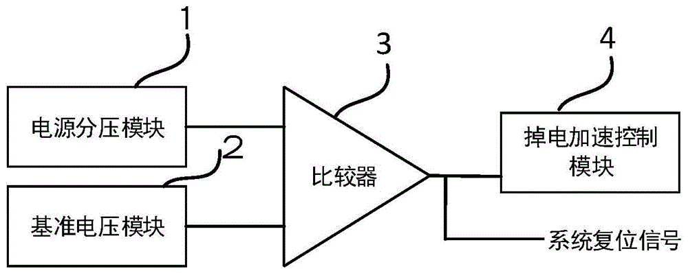
The invention provides a method and circuit for accelerating power-off and reset that can precisely control the power-off detection threshold. It has the following characteristics: (1) It can accurately and reliably detect the power-off event, and give the system reset signal and open the accelerated power-down circuit; it can stably and reliably solve the problem that the IC cannot be reset due to the incomplete power-down of the IC power supply. For the problem of starting up, the power supply voltage can be reduced to 0 within a very short time of no more than 10μs; (2) The power-off detection threshold can be precisely controlled, and it is not sensitive to the system power supply voltage and temperature, so it can also suppress the fluctuation of the system power supply Or the impact of temperature changes on the stability and reliability of IC power-off detection, to avoid IC falsely triggering system reset due to system power fluctuations or temperature changes. (3) The circuit of the present invention can work in ICs with a wide range of power supply domains, and can meet the requirements for system power supplies that need to be compatible with a wide range such as 1.8v-3.3v or 3.3v-5v.
Description
技术领域technical field
本发明涉及电子产品的放电电路领域,特别涉及一种精确控制检测阈值的加速掉电和复位方法及电路。The invention relates to the field of discharge circuits of electronic products, in particular to an accelerated power-down and reset method and circuit for precisely controlling a detection threshold.
背景技术Background technique
IC(Integrated Circuit)作为控制系统的核心元件,被用于众多控制系统中。当控制系统遭遇突然断电或者其他意外状况导致的IC掉电时,控制系统会快读响应并通过备用电源等方式再重新对IC进行上电。此时IC会经历一个短暂的掉电,再上电过程,这个掉电上电过程的时间最短可达到10毫秒的数量级。而IC在遭遇断电后,其电源电荷会依赖内部MOS管来泄放,在电源掉电至MOS阈值(一般约0.7v左右)附近时,由于MOS管关闭,掉电开始变得特别缓慢。一个典型的IC电源掉电曲线,从电源开始掉电到IC完全掉电到0,根据电源上的负载电容不同,可能需要几百毫秒,甚至是几秒。在遇到上述的快速掉电上电过程时,由于电源还没有完全掉电到0就要再次上电,这会导致IC无法完全复位,内部寄存器或者控制逻辑出错,进而导致无法正常启动。IC (Integrated Circuit), as the core component of the control system, is used in many control systems. When the control system encounters a sudden power failure or other unexpected situations that cause the IC to lose power, the control system will quickly read the response and re-power the IC through a backup power supply. At this time, the IC will experience a short power-off, and then power-on process. The shortest time of this power-off and power-on process can reach the order of magnitude of 10 milliseconds. After the IC encounters a power failure, its power supply charge will rely on the internal MOS tube to discharge. When the power supply is powered down to the vicinity of the MOS threshold (generally about 0.7v), the power down becomes very slow because the MOS tube is turned off. A typical IC power down curve, from the power down to the IC completely power down to 0, depending on the load capacitance on the power supply, it may take hundreds of milliseconds, or even a few seconds. When encountering the above-mentioned rapid power-off and power-on process, because the power supply has not been completely powered off to 0, it will be powered on again, which will cause the IC to not be completely reset, and the internal register or control logic will be wrong, which will lead to the failure to start normally.
发明内容Contents of the invention
本发明针对电源还没有完全掉电到0就要再次上电,这会导致IC无法完全复位,内部寄存器或者控制逻辑出错,进而导致无法正常启动的现有问题,提供了一种可以精确控制掉电检测阈值的加速掉电和复位的方法、电路及装置,具体如下。The present invention aims at the existing problems that the power supply will be powered on again before it is completely powered off to 0, which will cause the IC to be unable to be completely reset, internal registers or control logic errors, and thus lead to failure to start normally. The method, circuit and device for accelerating power-off and reset of the electrical detection threshold are as follows.
1.一种精确控制检测阈值的加速掉电和复位方法,包括以下步骤:1. A method for accelerating power-down and reset of a precise control detection threshold, comprising the following steps:
S100)生成跟随系统电源电压变化的分压电压及不随系统电源电压变化的参考电压;S100) Generate a divided voltage that follows the system power supply voltage change and a reference voltage that does not change with the system power supply voltage;
S200)比较跟随电压与参考电压的大小,若跟随电压小于参考电压,则继续执行以下步骤,否则结束;S200) Comparing the magnitude of the following voltage and the reference voltage, if the following voltage is less than the reference voltage, continue to perform the following steps, otherwise end;
S300)产生电路复位信号并对电路进行复位;S300) generating a circuit reset signal and resetting the circuit;
S400)在不超过10μs的极短时间内将电源电压加速降低至0。S400) Accelerating the reduction of the power supply voltage to 0 within a very short time of no more than 10 μs.
2.一种精确控制检测阈值的加速掉电和复位方法,步骤S400还包括以下前置步骤:2. An accelerated power-down and reset method for accurately controlling the detection threshold, step S400 also includes the following pre-steps:
S401)将系统电源电压降低至可预先设定的检测阈值电压。S401) Lowering the system power supply voltage to a preset detection threshold voltage.
3.一种精确控制检测阈值的加速掉电和复位电路,包括系统电源,电源分压电路,参考电压电路,比较电路和掉电加速控制电路;3. An accelerated power-down and reset circuit that precisely controls the detection threshold, including a system power supply, a power supply voltage divider circuit, a reference voltage circuit, a comparison circuit and a power-down acceleration control circuit;
所述系统电源与所述电源分压电路,参考电压电路,比较电路和掉电加速控制电路相连接;The system power supply is connected with the power supply voltage divider circuit, reference voltage circuit, comparison circuit and power-down acceleration control circuit;
所述电源分压电路输出端和参考电压电路的输出端分别与所述比较电路的两个输入端相连接;所述比较电路的输出端与所述掉电加速控制电路的输入端相连接;The output end of the power voltage divider circuit and the output end of the reference voltage circuit are respectively connected to the two input ends of the comparison circuit; the output end of the comparison circuit is connected to the input end of the power-down acceleration control circuit;
当系统电源掉电时,所述比较电路产生电路复位信号并使得所述掉电加速控制电路导通,所述掉电加速控制电路加速系统电源的掉电速度。When the system power supply is powered off, the comparison circuit generates a circuit reset signal and turns on the power-down acceleration control circuit, and the power-down acceleration control circuit accelerates the power-down speed of the system power supply.
4.一种精确控制检测阈值的加速掉电和复位电路,所述电源分压电路包括,第一电阻和第二电阻,其中第一电阻一端与所述系统电源相连,另一端与所述第二电阻一端串联连接并作为跟随电压的输出端,所述第二电阻另一端接地。4. An accelerated power-down and reset circuit that precisely controls the detection threshold, the power supply voltage divider circuit includes a first resistor and a second resistor, wherein one end of the first resistor is connected to the system power supply, and the other end is connected to the second resistor. One end of the two resistors is connected in series and serves as an output end following the voltage, and the other end of the second resistor is grounded.
5.一种精确控制检测阈值的加速掉电和复位电路,所述电源分压电路还可包括,第一MOS管和第二MOS管,其中,所述第一MOS管采用共漏极接法,其源极连接所述系统电源,其栅极及漏极连接第一电阻的一端,所述第二MOS管采用共漏极接法,其源极连接所述第一电阻的另一端并作为所述分压电路的输出端,输出分压电压,其栅极及漏极连接第二电阻的一端。5. An accelerated power-down and reset circuit that precisely controls the detection threshold, the power supply voltage divider circuit may also include a first MOS transistor and a second MOS transistor, wherein the first MOS transistor adopts a common drain connection , its source is connected to the system power supply, its gate and drain are connected to one end of the first resistor, the second MOS tube is connected to the common drain, its source is connected to the other end of the first resistor and used as The output end of the voltage divider circuit outputs a divided voltage, and its gate and drain are connected to one end of the second resistor.
6.一种精确控制检测阈值的加速掉电和复位电路,所述参考电压电路包括,第三电阻,第三MOS管和第四MOS管,所述第三电阻一端连接所述系统电源,另一端连接所述第三MOS管的漏极及栅极,所述第三MOS管采用共漏极接法,其源极作为所述参考电路的输出端,输出参考电压,源极与所述第四MOS管的漏极连接,所述第四MOS管的源极与系统电源连接,源极接地。6. An accelerated power-down and reset circuit that precisely controls the detection threshold, the reference voltage circuit includes a third resistor, a third MOS transistor and a fourth MOS transistor, one end of the third resistor is connected to the system power supply, and the other One end is connected to the drain and gate of the third MOS transistor, the third MOS transistor adopts a common drain connection method, and its source is used as the output end of the reference circuit to output a reference voltage, and the source is connected to the first The drains of the four MOS transistors are connected, the source of the fourth MOS transistor is connected to the system power supply, and the source is grounded.
7.一种精确控制检测阈值的加速掉电和复位电路,所述比较电路包括,第五MOS管,第六MOS管,第七MOS管,第八MOS管,第九MOS管,第十MOS管,第十一MOS管和第一比较器组成,其中,所述第五MOS管采用共漏极接法,其源极与系统电源连接,其栅极与所述第七MOS管的栅极连接,其漏极与所述第六MOS管的漏极连接,所述第六MOS管的栅极与参考电压的输出端连接,其源极与所述第八MOS管源极连接,所述第七MOS管的源极与所述系统电源连接,其漏极与所述第八MOS管的漏极及所述第九MOS管的栅极连接,所述第八MOS管的栅极与所述跟随电压的输出端连接,所述第九MOS管的源极与所述系统电源连接,其漏极与所述第十MOS管的漏极及所述第一比较器的输入端连接,所述第十MOS管的栅极与参考电压的输出端连接,其源极与所述第十一MOS管的漏极连接,所述第十一MOS管的栅极与所述系统电源相连接,其源极接地。7. An accelerated power-down and reset circuit that accurately controls the detection threshold, the comparison circuit includes a fifth MOS tube, a sixth MOS tube, a seventh MOS tube, an eighth MOS tube, a ninth MOS tube, and a tenth MOS tube tube, the eleventh MOS tube and the first comparator, wherein the fifth MOS tube adopts a common drain connection, its source is connected to the system power supply, and its gate is connected to the gate of the seventh MOS tube connected, its drain is connected to the drain of the sixth MOS transistor, the gate of the sixth MOS transistor is connected to the output terminal of the reference voltage, its source is connected to the source of the eighth MOS transistor, and the The source of the seventh MOS transistor is connected to the system power supply, its drain is connected to the drain of the eighth MOS transistor and the gate of the ninth MOS transistor, and the gate of the eighth MOS transistor is connected to the gate of the ninth MOS transistor. The output end of the following voltage is connected, the source of the ninth MOS transistor is connected to the system power supply, and its drain is connected to the drain of the tenth MOS transistor and the input end of the first comparator, so The gate of the tenth MOS transistor is connected to the output terminal of the reference voltage, the source thereof is connected to the drain of the eleventh MOS transistor, and the gate of the eleventh MOS transistor is connected to the system power supply, Its source is grounded.
8.一种精确控制检测阈值的加速掉电和复位电路,所述掉电加速控制电路包括,第一电容,第一二极管,第一反相器,第十二MOS管,所述第一电容一端接地,另一端与所述第一二极管负极连接,所述第一二极管正极与所述系统电源连接,所述第一反相器的输入端与所述第一比较器的输出端连接,其输出端与所述第十二MOS管的栅极连接,所述第十二MOS管的漏极与所述系统电源连接,其源极接地。8. An accelerated power-down and reset circuit that accurately controls the detection threshold, the power-down acceleration control circuit includes a first capacitor, a first diode, a first inverter, a twelfth MOS tube, and the first One end of a capacitor is grounded, the other end is connected to the cathode of the first diode, the anode of the first diode is connected to the system power supply, the input end of the first inverter is connected to the first comparator The output end of the MOS transistor is connected to the gate of the twelfth MOS transistor, the drain of the twelfth MOS transistor is connected to the system power supply, and the source is grounded.
9.一种精确控制检测阈值的加速掉电和复位装置,包括以下模块:9. An accelerated power-down and reset device that precisely controls the detection threshold, comprising the following modules:
生成模块,用于生成跟随系统电源电压变化的分压电压及不随系统电源电压变化的参考电压;A generating module, configured to generate a divided voltage that follows changes in the system power supply voltage and a reference voltage that does not change with the system power supply voltage;
比较模块,用于比较跟随电压与参考电压的大小,若跟随电压小于参考电压,则启动复位模块和加速掉电模块;The comparison module is used to compare the magnitude of the following voltage and the reference voltage, and if the following voltage is less than the reference voltage, start the reset module and the accelerated power-down module;
复位模块,用于产生电路复位信号并对电路进行复位;The reset module is used to generate a circuit reset signal and reset the circuit;
加速掉电模块,用于在不超过10μs的极短时间内将电源电压加速降低至0。The accelerated power-down module is used to accelerate the power supply voltage down to 0 within a very short time of no more than 10μs.
10.一种计算机可读存储介质,其上存储有计算机指令,其特征在于该指令被处理器执行时实现如权利要求1至2中任一项所述的方法的步骤。10. A computer-readable storage medium, on which computer instructions are stored, characterized in that the steps of the method according to any one of
本发明可以准确可靠地检测掉电事件,并给出系统复位信号和开启加速掉电电路,在不超过10μs级的极短时间内将电源电压加速降低至0,可以稳定可靠地解决由于IC电源掉电不彻底而引起的IC无法复位导致的无法开机的问题。The present invention can accurately and reliably detect the power-down event, and give the system reset signal and open the accelerated power-down circuit, and accelerate the power supply voltage down to 0 in a very short time of no more than 10 μs, which can stably and reliably solve the problem of IC power failure The problem that the IC cannot be reset due to incomplete power failure causes the problem that the device cannot be turned on.
附图说明Description of drawings
图1所示为本申请所提出的一种精确控制检测阈值的加速掉电和复位方法一个实施例的流程图;Fig. 1 shows the flowchart of an embodiment of a method for accelerating power-down and reset of a precise control detection threshold proposed by the present application;
图2所示为本申请所提出的一种精确控制检测阈值的加速掉电和复位电路的电源分压电路图;Fig. 2 shows the power voltage divider circuit diagram of a kind of accelerated power-down and reset circuit of precise control detection threshold proposed by the present application;
图3所示为本申请所提出的一种精确控制检测阈值的加速掉电和复位电路的参考电压电路图;Fig. 3 shows the reference voltage circuit diagram of a kind of accelerated power-down and reset circuit that precisely controls the detection threshold proposed by the present application;
图4所示为本申请所提出的一种精确控制检测阈值的加速掉电和复位电路的比较电路电路图;Fig. 4 shows a comparison circuit circuit diagram of a kind of accelerated power-down and reset circuit for accurately controlling the detection threshold proposed by the present application;
图5所示为本申请所提出的一种精确控制检测阈值的加速掉电和复位电路的掉电加速控制电路图;Fig. 5 shows the power-down acceleration control circuit diagram of a kind of accelerated power-down and reset circuit with precise control detection threshold proposed by the present application;
图6所示为本申请所提出的一种精确控制检测阈值的加速掉电和复位电路示意图;Figure 6 shows a schematic diagram of an accelerated power-down and reset circuit for precisely controlling the detection threshold proposed by the present application;
图7所示为本申请所提出的一种精确控制检测阈值的加速掉电和复位装置的框架图;Fig. 7 shows the frame diagram of a kind of accelerated power-down and reset device that precisely controls the detection threshold proposed by the present application;
图8所示为本申请所提出的一种精确控制检测阈值的加速掉电和复位电路的掉电曲线对比图。FIG. 8 is a comparison diagram of power-down curves of an accelerated power-down and reset circuit with precisely controlled detection thresholds proposed in the present application.
具体实施方式Detailed ways
以下将结合实施例和附图对本发明的构思、具体结构及产生的技术效果进行清楚、完整的描述,以充分地理解本发明的目的、方案和效果。需要说明的是,在不冲突的情况下,本申请中的实施例及实施例中的特征可以相互组合。附图中各处使用的相同的附图标记指示相同或相似的部分。The idea, specific structure and technical effects of the present invention will be clearly and completely described below in conjunction with the embodiments and accompanying drawings, so as to fully understand the purpose, scheme and effect of the present invention. It should be noted that, in the case of no conflict, the embodiments in the present application and the features in the embodiments can be combined with each other. The same reference numbers are used throughout the drawings to indicate the same or similar parts.
在说明书的结论部分中特别指出并清楚地要求保护本发明提出的主题。然而,当结合附图进行阅读时,通过参考以下详细描述,可以最好地理解本发明的组织和操作方法以及其目的,特征和优点。The subject matter presented herein is particularly pointed out and distinctly claimed in the concluding portion of the specification. However, the organization and method of operation of the invention, together with its objects, features and advantages, are best understood by referring to the following detailed description when read with the accompanying drawings.
因为本发明的所示实施例可以在大多数情况下使用本领域技术人员已知的电子部件和电路来实现,所以细节将只在如上所述认为必要的程度上进行解释,以便理解本发明的基本概念,以免混淆或分散本发明的教导。Since the illustrated embodiments of the invention can in most cases be implemented using electronic components and circuits known to those skilled in the art, details will be explained only to the extent deemed necessary as described above in order to understand the principles of the invention. basic concepts so as not to obscure or distract from the teachings of the present invention.
参照图1所示的一种精确控制检测阈值的加速掉电和复位方法的流程图,本发明提出一种精确控制检测阈值的加速掉电和复位方法,包括以下步骤:With reference to the flow chart of a kind of accelerated power-off and reset method of accurately controlling the detection threshold shown in Figure 1, the present invention proposes a kind of accelerated power-off and reset method of accurately controlling the detection threshold, comprising the following steps:
S100)生成跟随系统电源电压变化的分压电压及不随系统电源电压变化的参考电压;S100) Generate a divided voltage that follows the system power supply voltage change and a reference voltage that does not change with the system power supply voltage;
S200)比较跟随电压与参考电压的大小,若跟随电压小于参考电压,则继续执行以下步骤,否则结束;S200) Comparing the magnitude of the following voltage and the reference voltage, if the following voltage is less than the reference voltage, continue to perform the following steps, otherwise end;
S300)产生电路复位信号并对电路进行复位;S300) generating a circuit reset signal and resetting the circuit;
S400)在不超过10μs的极短时间内将电源电压加速降低至0。S400) Accelerating the reduction of the power supply voltage to 0 within a very short time of no more than 10 μs.
具体地,若检测出跟随电压小于参考电压,则可判断为电源掉电,通过合理设置跟随系统电源电压变化的分压电压及不随系统电源电压变化的参考电压,则可准确可靠地检测掉电事件。Specifically, if it is detected that the following voltage is lower than the reference voltage, it can be judged as a power failure. By reasonably setting the divided voltage that follows the system power supply voltage and the reference voltage that does not change with the system power supply voltage, the power failure can be detected accurately and reliably. event.
具体地,步骤S400还包括以下前置步骤:Specifically, step S400 also includes the following pre-steps:
S401)将系统电源电压降低至可预先设定的检测阈值电压。S401) Lowering the system power supply voltage to a preset detection threshold voltage.
具体地,参照图8(b),是加入本发明的电路的掉电曲线,由图中可以看出,系统电源电压vcc在t0时刻开始下降,到t1时刻下降到可预先设定的检测阈值电压Vth,并最终在t2时刻降至0,经过实验证明,从t1时刻到t2时刻所经历的时间不超过10μs,即在0到10μs之间完成加速掉电过程。Specifically, referring to Fig. 8(b), it is the power-down curve of the circuit of the present invention. It can be seen from the figure that the system power supply voltage vcc begins to drop at time t0, and drops to a preset detection threshold at time t1 The voltage Vth, and finally drops to 0 at the time t2. Experiments have proved that the time from the time t1 to the time t2 does not exceed 10 μs, that is, the accelerated power-down process is completed between 0 and 10 μs.
进一步,检测阈值电压Vth的计算过程为:Further, the calculation process of the detection threshold voltage Vth is:
Vf=R2/(R1+R2)×vcc,其中Vf为跟随电压,vcc为系统电源电压,R1,R2分别为图2中的第一电阻和第二电阻的电阻值。Vf=R2/(R1+R2)×vcc, where Vf is the follower voltage, vcc is the system power supply voltage, R1 and R2 are the resistance values of the first resistor and the second resistor in FIG. 2 respectively.
当vcc下降至Vth时,Vf=Vb,所以此时Vf=R2/(R1+R2)×Vth,其中Vb为参考电压,When vcc drops to Vth, Vf=Vb, so at this time Vf=R2/(R1+R2)×Vth, where Vb is the reference voltage,
由此,可计算出Vth=(R1+R2)/R2×VbFrom this, Vth=(R1+R2)/R2×Vb can be calculated
当图2中的电路尺寸确定后,参考电压Vb就确定了,此时可以通过调节R1和R2的分压比例来调整检测阈值电压Vth,即,可以根据实际的需要检测阈值电压,通过电路的设计,使得当系统电源电压低于检测阈值电压时,启动掉电加速控制模块,达到快速掉电的目的。When the size of the circuit in Figure 2 is determined, the reference voltage Vb is determined. At this time, the detection threshold voltage Vth can be adjusted by adjusting the voltage division ratio of R1 and R2, that is, the threshold voltage can be detected according to actual needs. Through the circuit It is designed so that when the system power supply voltage is lower than the detection threshold voltage, the power-down acceleration control module is started to achieve the purpose of fast power-down.
具体地,所述极短的不超过10μs(微秒)的时间是根据实际的测试情况得出的。Specifically, the extremely short time of no more than 10 μs (microsecond) is obtained according to actual test conditions.
优选地,在实验环境中,所述不超过10μs(微秒)的时间可进一步缩短到6μs。Preferably, in an experimental environment, the time of no more than 10 μs (microsecond) can be further shortened to 6 μs.
具体地,所述电路复位信号为比较器输出的低电平信号。Specifically, the circuit reset signal is a low-level signal output by the comparator.
电源电压vcc正常工作时,Vf值远大于Vb值,比较器的输出信号vcc_det为高电平,加速掉电电路关闭。当电源电压vcc开始下降时,Vf小于Vb时,比较器输出信号vcc_det为低电平,此时IC使用vcc_det作为复位信号对IC内部的逻辑电路进行复位,同时开启加速掉电电路,对电源vcc进行电荷泄放,达到快速掉电的目的。When the power supply voltage vcc works normally, the value of Vf is far greater than the value of Vb, the output signal vcc_det of the comparator is at a high level, and the accelerated power-down circuit is turned off. When the power supply voltage vcc starts to drop, when Vf is less than Vb, the comparator output signal vcc_det is low level, at this time, the IC uses vcc_det as a reset signal to reset the logic circuit inside the IC, and at the same time, the accelerated power-down circuit is turned on, and the power supply vcc Perform charge discharge to achieve the purpose of rapid power down.
具体地,参照图3至图7,本发明的整体电路架构如图7所示,由4个分电路模块组成。Specifically, referring to FIG. 3 to FIG. 7 , the overall circuit architecture of the present invention is shown in FIG. 7 and consists of four sub-circuit modules.
参照图2,是本发明的分压电路的电路图,图中分压电路包括第一电阻(R1)和第二电阻(R2),其中第一电阻一端与所述系统电源相连,另一端与所述第二电阻一端串联连接并作为跟随电压的输出端,所述第二电阻另一端接地。Referring to Fig. 2, it is the circuit diagram of the voltage divider circuit of the present invention, the voltage divider circuit comprises a first resistor (R1) and a second resistor (R2) among the figure, wherein one end of the first resistor is connected with the described system power supply, and the other end is connected with the described system power supply One end of the second resistor is connected in series and serves as an output end following the voltage, and the other end of the second resistor is grounded.
该分压电路通过电压电路来获得一个电源vcc的分压信号Vf,用于跟随电源变化,当电源掉电时,Vf也要跟随vcc下降。图2给出了两种实现方式,图2(a)产生的分压Vf=R2/(R1+R2)×vcc;若要产生一个1/2的vcc的分压,也可以使用图2(b)的方式实现,其中图2(b)包括第一MOS管(M1)和第二MOS管(M2),其中,所述第一MOS管采用共漏极接法,其源极连接所述系统电源,其栅极及漏极连接第一电阻的一端,所述第二MOS管采用共漏极接法,其源极连接所述第一电阻的另一端并作为所述分压电路的输出端,输出分压电压,其栅极及漏极连接第二电阻的一端。The voltage divider circuit obtains a voltage divider signal Vf of the power supply vcc through the voltage circuit, which is used to follow the change of the power supply. When the power supply is powered off, the Vf also follows the drop of the vcc. Figure 2 shows two implementations, the divided voltage Vf=R2/(R1+R2)×vcc generated in Figure 2(a); if you want to generate a divided voltage of 1/2 vcc, you can also use Figure 2 ( b) is implemented, wherein Fig. 2(b) includes a first MOS transistor (M1) and a second MOS transistor (M2), wherein the first MOS transistor adopts a common drain connection method, and its source is connected to the System power supply, its gate and drain are connected to one end of the first resistor, the second MOS tube is connected to the common drain, and its source is connected to the other end of the first resistor as the output of the voltage divider circuit The terminal outputs the divided voltage, and its gate and drain are connected to one terminal of the second resistor.
参照图3,是本发明的参考电压的电路图,所述参考电压电路包括,第三电阻(R3),第三MOS管(M3)和第四MOS管(M4),所述第三电阻一端连接所述系统电源,另一端连接所述第三MOS管的漏极及栅极,所述第三MOS管采用共漏极接法,其源极作为所述参考电路的输出端,输出参考电压,源极与所述第四MOS管的漏极连接,所述第四MOS管的源极与系统电源连接,源极接地。With reference to Fig. 3, it is the circuit diagram of the reference voltage of the present invention, and described reference voltage circuit comprises, the 3rd resistor (R3), the 3rd MOS tube (M3) and the 4th MOS tube (M4), described 3rd resistor one end connects The other end of the system power supply is connected to the drain and gate of the third MOS transistor, the third MOS transistor adopts a common drain connection method, and its source is used as the output terminal of the reference circuit to output a reference voltage, The source is connected to the drain of the fourth MOS transistor, the source of the fourth MOS transistor is connected to the system power supply, and the source is grounded.
所述参考电压电路产生一个对系统电源波动和温度变化不敏感的参考电压Vb,这就意味着,在系统电源掉电时或者温度变化时,产生的Vb还可以保持稳定,或者变化很小。图4是一种实现形式,由一个较大的电阻R3和两个MOS管M3和M4组成。R3采用较大阻值,这样支路电流I就会很小;M3采用二极管的连接方式,工作在亚阈值区,所以M3上的压降约等于一个MOS阈值;M4的栅极接电源电压,M4工作在线性区,等效成一个电阻Rx,产生的参考电压Vb就等于M3的阈值电压Vth3加上M4上的压降Vds4。即,Vb=Vth3+Vds4,其中Vds=Rx×I。The reference voltage circuit generates a reference voltage Vb that is insensitive to system power fluctuations and temperature changes, which means that when the system power supply is powered off or the temperature changes, the generated Vb can remain stable or change very little. Figure 4 is an implementation form, which consists of a larger resistor R3 and two MOS transistors M3 and M4. R3 adopts a large resistance value, so that the branch current I will be very small; M3 adopts a diode connection mode and works in the sub-threshold region, so the voltage drop on M3 is approximately equal to a MOS threshold; the gate of M4 is connected to the power supply voltage, M4 works in the linear region, which is equivalent to a resistor Rx, and the generated reference voltage Vb is equal to the threshold voltage Vth3 of M3 plus the voltage drop Vds4 on M4. That is, Vb=Vth3+Vds4, where Vds=Rx×I.
(1)当电源vcc开始掉电时,R3上的压降会变小,支路电流I也会变小,但是对于工作在亚阈值区的M3来说,压降变化非常小,同时由于M4的栅极电压随vcc的下降,M4的等效电阻Rx变大,这样Vds4会由于Rx的增加,与I的变小形成对冲作用,所以Vds4也基本可以保持稳定。这样Vb就几乎不随电源vcc掉电的影响。(1) When the power supply vcc starts to lose power, the voltage drop on R3 will become smaller, and the branch current I will also become smaller, but for M3 working in the sub-threshold region, the change in voltage drop is very small, and because M4 As the gate voltage of VCC decreases, the equivalent resistance Rx of M4 increases, so that Vds4 will form a hedging effect with the decrease of I due to the increase of Rx, so Vds4 can basically remain stable. In this way, Vb is almost not affected by power failure of the power supply vcc.
(2)MOS管阈值是随着温度增加而减小,而工作在线性区的MOS管阻抗是随温度增加而增加的。这样的话,只要M4的尺寸取值合适,那么M3的阈值的变化量刚好和M4的压降变化相抵消。这样产生的Vb也几乎不随温度变化的影响。(2) The threshold value of the MOS tube decreases as the temperature increases, while the impedance of the MOS tube working in the linear region increases as the temperature increases. In this case, as long as the size of M4 is appropriate, the variation of the threshold of M3 just offsets the variation of the pressure drop of M4. Vb thus generated is also hardly affected by temperature changes.
参照图4,是本发明的比较电路的电路图,所述比较电路包括,第五MOS管(M5),第六MOS管(M6),第七MOS管(M7),第八MOS管(M8),第九MOS管(M9),第十MOS管(M10),第十一MOS管(M11)和第一比较器(BUF1)组成,其中,所述第五MOS管采用共漏极接法,其源极与系统电源连接,其栅极与所述第七MOS管的栅极连接,其漏极与所述第六MOS管的漏极连接,所述第六MOS管的栅极与参考电压的输出端连接,其源极与所述第八MOS管源极连接,所述第七MOS管的源极与所述系统电源连接,其漏极与所述第八MOS管的漏极及所述第九MOS管的栅极连接,所述第八MOS管的栅极与所述跟随电压的输出端连接,所述第九MOS管的源极与所述系统电源连接,其漏极与所述第十MOS管的漏极及所述第一比较器的输入端连接,所述第十MOS管的栅极与参考电压的输出端连接,其源极与所述第十一MOS管的漏极连接,所述第十一MOS管的栅极与所述系统电源相连接,其源极接地。With reference to Fig. 4, it is the circuit diagram of the comparison circuit of the present invention, and described comparison circuit comprises, the 5th MOS tube (M5), the 6th MOS tube (M6), the 7th MOS tube (M7), the 8th MOS tube (M8) , the ninth MOS transistor (M9), the tenth MOS transistor (M10), the eleventh MOS transistor (M11) and the first comparator (BUF1), wherein the fifth MOS transistor adopts a common drain connection method, Its source is connected to the system power supply, its gate is connected to the gate of the seventh MOS transistor, its drain is connected to the drain of the sixth MOS transistor, and the gate of the sixth MOS transistor is connected to the reference voltage connected to the output terminal, its source is connected to the source of the eighth MOS transistor, the source of the seventh MOS transistor is connected to the system power supply, and its drain is connected to the drain of the eighth MOS transistor and the The gate of the ninth MOS transistor is connected, the gate of the eighth MOS transistor is connected to the output terminal of the following voltage, the source of the ninth MOS transistor is connected to the system power supply, and its drain is connected to the The drain of the tenth MOS transistor is connected to the input end of the first comparator, the gate of the tenth MOS transistor is connected to the output end of the reference voltage, and its source is connected to the drain of the eleventh MOS transistor pole connection, the gate of the eleventh MOS transistor is connected to the system power supply, and its source is grounded.
该比较电路实现比较器功能,但是需要比较器在掉电加速模块开启之前能够保持正常工作,也就是说需要在电源电压降至图8(b)中的Vth时依然保持工作。图4即为一种可以满足要求的比较器电路实现方法,电源电压vcc正常工作时,Vf值远大于Vb值,比较器的输出信号vcc_det为高电平,加速掉电电路关闭。当电源电压vcc开始下降时,Vf小于Vb时,比较器输出信号vcc_det为低电平,此时IC使用vcc_det作为复位信号对IC内部的逻辑电路进行复位,同时开启加速掉电电路,对电源vcc进行电荷泄放,达到快速掉电的目的。The comparison circuit implements the comparator function, but the comparator needs to be able to keep working normally before the power-down acceleration module is turned on, that is to say, it needs to keep working when the power supply voltage drops to Vth in Figure 8(b). Figure 4 is a comparator circuit implementation method that can meet the requirements. When the power supply voltage vcc is working normally, the value of Vf is much greater than the value of Vb. The output signal vcc_det of the comparator is at a high level, and the accelerated power-down circuit is turned off. When the power supply voltage vcc starts to drop, when Vf is less than Vb, the comparator output signal vcc_det is low level, at this time, the IC uses vcc_det as a reset signal to reset the logic circuit inside the IC, and at the same time, the accelerated power-down circuit is turned on, and the power supply vcc Perform charge discharge to achieve the purpose of rapid power down.
参照图5,是本发明的掉电加速控制电路的电路图,所述掉电加速控制电路包括,第一电容(C1),第一二极管(D1),第一反相器(INV1),第十二MOS管(M12),所述第一电容一端接地,另一端与所述第一二极管负极连接,所述第一二极管正极与所述系统电源连接,所述第一反相器的输入端与所述第一比较器的输出端连接,其输出端与所述第十二MOS管的栅极连接,所述第十二MOS管的漏极与所述系统电源连接,其源极接地。Referring to Fig. 5, it is a circuit diagram of the power-down acceleration control circuit of the present invention, and the power-down acceleration control circuit includes a first capacitor (C1), a first diode (D1), a first inverter (INV1), In the twelfth MOS transistor (M12), one end of the first capacitor is grounded, the other end is connected to the cathode of the first diode, the anode of the first diode is connected to the system power supply, and the first inverter The input terminal of the phaser is connected to the output terminal of the first comparator, the output terminal thereof is connected to the gate of the twelfth MOS transistor, and the drain of the twelfth MOS transistor is connected to the system power supply, Its source is grounded.
掉电加速控制电路,受比较电路的输出信号vcc_det控制。图5是掉电加速电路的实现形式。电源vcc通过二极管D1对节点vcc_in进行充电,同时vcc_in节点有一个电容C1来存储电荷,vcc_in的电位为vcc-Vthd,Vthd为D1的阈值电压。D1也可以使用一个二极管连接的PMOS实现。当电源vcc掉电时,由于vcc_in节点无直流通路,所以电荷只能通过下面的反相器INV1来慢慢漏掉,所以vcc_in节点在相当长时间内都会保持vcc-Vthd的电位。当比较器输出的vcc_det信号由1变为0之后,INV1输出的控制信号ctrl由0变为1,此时MOS管M12导通,开始对vcc进行加速掉电,直到vcc掉电至0。The power-down acceleration control circuit is controlled by the output signal vcc_det of the comparison circuit. Fig. 5 is the implementation form of the power-down acceleration circuit. The power supply vcc charges the node vcc_in through the diode D1. At the same time, the vcc_in node has a capacitor C1 to store the charge. The potential of vcc_in is vcc-Vthd, and Vthd is the threshold voltage of D1. D1 can also be implemented using a diode-connected PMOS. When the power supply vcc is powered off, since the vcc_in node has no DC path, the charge can only be slowly leaked through the inverter INV1 below, so the vcc_in node will maintain the potential of vcc-Vthd for a long time. When the vcc_det signal output by the comparator changes from 1 to 0, the control signal ctrl output by INV1 changes from 0 to 1. At this time, the MOS transistor M12 is turned on, and the vcc is accelerated to power down until vcc is powered down to 0.
在IC中加入本发明之后,电源的掉电曲线由图8(a)变为图8(b),即在vcc掉电至Vth时,会迅速掉电至0。可以将电源的加速掉电时间缩短到10毫秒(us)以内。After the present invention is added to the IC, the power-down curve of the power supply is changed from Fig. 8(a) to Fig. 8(b), that is, when vcc is powered down to Vth, it will be powered down to 0 rapidly. The accelerated power-down time of the power supply can be shortened to less than 10 milliseconds (us).
掉电检测阈值Vth的计算过程:The calculation process of the power-down detection threshold Vth:
Vf=R2/(R1+R2)×vccVf=R2/(R1+R2)×vcc
当vcc下降至Vth时,Vf=Vb,所以此时Vf=R2/(R1+R2)×VthWhen vcc drops to Vth, Vf=Vb, so at this time Vf=R2/(R1+R2)×Vth
由此,可计算出Vth=(R1+R2)/R2×VbFrom this, Vth=(R1+R2)/R2×Vb can be calculated
当图2中的电路尺寸确定后,Vb就确定了,此时可以通过调节R1和R2的分压比例来调整检测阈值Vth。When the size of the circuit in Figure 2 is determined, Vb is determined. At this time, the detection threshold Vth can be adjusted by adjusting the voltage division ratio of R1 and R2.
由此,本发明实现了掉电检测阈值可精确控制的加速掉电和复位电路。Thus, the present invention realizes an accelerated power-down and reset circuit whose power-down detection threshold can be precisely controlled.
参照图7所示的一种精确控制检测阈值的加速掉电和复位装置的框架图,包括以下模块:With reference to the frame diagram of an accelerated power-down and reset device for accurately controlling the detection threshold shown in Figure 7, it includes the following modules:
生成模块,用于生成跟随系统电源电压变化的分压电压及不随系统电源电压变化的参考电压;A generating module, configured to generate a divided voltage that follows changes in the system power supply voltage and a reference voltage that does not change with the system power supply voltage;
比较模块,用于比较跟随电压与参考电压的大小,若跟随电压小于参考电压,则启动复位模块和加速掉电模块;The comparison module is used to compare the magnitude of the following voltage and the reference voltage, and if the following voltage is less than the reference voltage, start the reset module and the accelerated power-down module;
复位模块,用于产生电路复位信号并对电路进行复位;The reset module is used to generate a circuit reset signal and reset the circuit;
加速掉电模块,用于在不超过10μs的极短时间内将电源电压加速降低至0。The accelerated power-down module is used to accelerate the power supply voltage down to 0 within a very short time of no more than 10μs.
本发明电路可以工作在宽电源域范围的IC中,对于需要兼容类似1.8v~3.3v或者3.3v~5v等宽范围的电源都满足要求。The circuit of the invention can work in an IC with a wide range of power supply domains, and meets the requirements for being compatible with power supplies with a wide range such as 1.8v-3.3v or 3.3v-5v.
在本说明书的描述中,参考术语“一个实施方式”、“一些实施方式”、“一个实施例”、“一些实施例”、“示例”、“具体示例”、或“一些示例”等的描述意指结合该实施例或示例描述的具体特征、结构、材料或者特点包含于本发明的至少一个实施例或示例中。在本说明书中,对上述术语的示意性表述不一定指的是相同的实施例或示例。而且,描述的具体特征、结构、材料或者特点可以在任何的一个或多个实施例或示例中以合适的方式结合。In the description of this specification, reference is made to descriptions of the terms "one embodiment", "some embodiments", "an embodiment", "some embodiments", "examples", "specific examples", or "some examples" etc. It means that a specific feature, structure, material or characteristic described in connection with the embodiment or example is included in at least one embodiment or example of the present invention. In this specification, schematic representations of the above terms do not necessarily refer to the same embodiment or example. Furthermore, the specific features, structures, materials or characteristics described may be combined in any suitable manner in any one or more embodiments or examples.
本发明并不限于上文讨论的实施方式。以上对具体实施方式的描述旨在于为了描述和说明本发明涉及的技术方案。基于本发明启示的显而易见的变换或替代也应当被认为落入本发明的保护范围。以上的具体实施方式用来揭示本发明的最佳实施方法,以使得本领域的普通技术人员能够应用本发明的多种实施方式以及多种替代方式来达到本发明的目的。The invention is not limited to the embodiments discussed above. The above description of specific implementations is intended to describe and illustrate the technical solutions involved in the present invention. Obvious changes or substitutions based on the teachings of the present invention should also be deemed to fall within the protection scope of the present invention. The above specific implementation manners are used to reveal the best implementation method of the present invention, so that those skilled in the art can apply various implementation manners and various alternative modes of the present invention to achieve the purpose of the present invention.
Claims (9)


Priority Applications (1)
| Application Number | Priority Date | Filing Date | Title |
|---|---|---|---|
| CN201811181065.5A CN109617543B (en) | 2018-10-11 | 2018-10-11 | A method and circuit for accelerating power-down and reset with precise control of detection threshold |
Applications Claiming Priority (1)
| Application Number | Priority Date | Filing Date | Title |
|---|---|---|---|
| CN201811181065.5A CN109617543B (en) | 2018-10-11 | 2018-10-11 | A method and circuit for accelerating power-down and reset with precise control of detection threshold |
Publications (2)
| Publication Number | Publication Date |
|---|---|
| CN109617543A CN109617543A (en) | 2019-04-12 |
| CN109617543B true CN109617543B (en) | 2023-06-27 |
Family
ID=66001758
Family Applications (1)
| Application Number | Title | Priority Date | Filing Date |
|---|---|---|---|
| CN201811181065.5A Active CN109617543B (en) | 2018-10-11 | 2018-10-11 | A method and circuit for accelerating power-down and reset with precise control of detection threshold |
Country Status (1)
| Country | Link |
|---|---|
| CN (1) | CN109617543B (en) |
Families Citing this family (1)
| Publication number | Priority date | Publication date | Assignee | Title |
|---|---|---|---|---|
| CN112671205A (en) * | 2019-10-16 | 2021-04-16 | 中兴通讯股份有限公司 | Time sequence control device and method and single-board power supply |
Citations (7)
| Publication number | Priority date | Publication date | Assignee | Title |
|---|---|---|---|---|
| US4611126A (en) * | 1984-10-04 | 1986-09-09 | Werkzeugmaschinenfabrik Oerlikon-Buehrle Ag | Power on/off reset generator |
| JPH0474208A (en) * | 1990-07-16 | 1992-03-09 | Nissan Motor Co Ltd | Power-on reset circuit |
| CN1713526A (en) * | 2004-06-15 | 2005-12-28 | 富士通株式会社 | Reset circuit |
| CN102931959A (en) * | 2012-02-13 | 2013-02-13 | 北京七芯中创科技有限公司 | Circuit for quickly discharging power-on resetting circuit subjected to power failure |
| CN103095265A (en) * | 2012-11-13 | 2013-05-08 | 长沙景嘉微电子股份有限公司 | Automatic reset detection circuit for power up and power failure |
| US9407254B1 (en) * | 2014-10-15 | 2016-08-02 | Xilinx, Inc. | Power on-reset with built-in hysteresis |
| CN107835006A (en) * | 2017-12-19 | 2018-03-23 | 电子科技大学 | Low-power consumption electrification reset power-off reset circuit |
-
2018
- 2018-10-11 CN CN201811181065.5A patent/CN109617543B/en active Active
Patent Citations (7)
| Publication number | Priority date | Publication date | Assignee | Title |
|---|---|---|---|---|
| US4611126A (en) * | 1984-10-04 | 1986-09-09 | Werkzeugmaschinenfabrik Oerlikon-Buehrle Ag | Power on/off reset generator |
| JPH0474208A (en) * | 1990-07-16 | 1992-03-09 | Nissan Motor Co Ltd | Power-on reset circuit |
| CN1713526A (en) * | 2004-06-15 | 2005-12-28 | 富士通株式会社 | Reset circuit |
| CN102931959A (en) * | 2012-02-13 | 2013-02-13 | 北京七芯中创科技有限公司 | Circuit for quickly discharging power-on resetting circuit subjected to power failure |
| CN103095265A (en) * | 2012-11-13 | 2013-05-08 | 长沙景嘉微电子股份有限公司 | Automatic reset detection circuit for power up and power failure |
| US9407254B1 (en) * | 2014-10-15 | 2016-08-02 | Xilinx, Inc. | Power on-reset with built-in hysteresis |
| CN107835006A (en) * | 2017-12-19 | 2018-03-23 | 电子科技大学 | Low-power consumption electrification reset power-off reset circuit |
Non-Patent Citations (1)
| Title |
|---|
| MCU电源监控芯片的设计与实现;吴斯敏;《中国优秀硕士论文电子期刊网》;20090515;第1-65页 * |
Also Published As
| Publication number | Publication date |
|---|---|
| CN109617543A (en) | 2019-04-12 |
Similar Documents
| Publication | Publication Date | Title |
|---|---|---|
| US10503189B1 (en) | Voltage regulator and dynamic bleeder current circuit | |
| US10090833B2 (en) | Low power reset circuit | |
| US7417476B1 (en) | Power-on-reset circuit with output reset to ground voltage during power off | |
| CN102455730A (en) | Semiconductor integrated circuit for regulator | |
| JP2000031807A (en) | Power-on reset circuit for integrated circuits | |
| CN110957713B (en) | Electrostatic discharge clamping circuit | |
| TW201509086A (en) | Voltage regulator soft start | |
| CN115189681A (en) | Power-on reset circuit capable of stabilizing pulse output | |
| WO2020018681A1 (en) | Power-on reset circuit | |
| US7099223B2 (en) | Semiconductor memory device | |
| JP2009098801A (en) | Power supply circuit and internal power supply voltage generation method using the same | |
| US20180204626A1 (en) | Circuits For Bleeding Supply Voltage From A Device In A Power Down State | |
| CN112187232A (en) | Power-on detection circuit and power-on detection method | |
| US10367499B2 (en) | Power supply ready indicator circuit | |
| WO2008064030A2 (en) | Method for providing a power on reset signal with a logarithmic current compared to a quadratic current | |
| US20160294193A1 (en) | Voltage generator | |
| CN108111150B (en) | Power-on reset circuit, integrated circuit and EEPROM system | |
| CN112947661A (en) | Quick power-on voltage stabilizer circuit and method | |
| EP2899523B1 (en) | Circuit designs for induced transient immunity | |
| JP4080696B2 (en) | Semiconductor integrated circuit | |
| CN108776501B (en) | Multiplexing circuit of LDO and POR | |
| US10691151B2 (en) | Devices and methods for dynamic overvoltage protection in regulators | |
| US20120062284A1 (en) | Low-voltage data retention circuit and method | |
| JP5971604B2 (en) | Voltage detection circuit | |
| CN113972637B (en) | Discharge device |
Legal Events
| Date | Code | Title | Description |
|---|---|---|---|
| PB01 | Publication | ||
| PB01 | Publication | ||
| SE01 | Entry into force of request for substantive examination | ||
| SE01 | Entry into force of request for substantive examination | ||
| GR01 | Patent grant | ||
| GR01 | Patent grant |