Detailed Description
Next, an image display device according to each embodiment will be described with reference to the drawings. In the following, the one-frame period is a period required for refreshing (rewriting a display image) one screen amount, and the length of the "one-frame period" is the length of the one-frame period (16.67ms) in a general display device having a refresh rate of 60 Hz. The term "calculation" included in the following description includes "calculation result obtained by using an arithmetic unit" and "calculation result obtained by storing calculation result in advance in a table and extracting the table".
<1 > first embodiment >
<1.1 Overall configuration >
Fig. 1 is a block diagram showing a configuration of an image display device according to a first embodiment. The image display device 1 shown in fig. 1 includes an image data conversion unit 10 and a display unit 20. The image data conversion unit 10 includes a parameter storage unit 11 and a driving image data calculation unit 33. The display unit 20 includes: a liquid crystal panel 24 as a light modulation section; a backlight 25 as a light source unit including a red light source 27r, a green light source 27g, a blue light source 27b, and a light guide plate; a timing control circuit 21; a panel drive circuit 22 as a light modulation section drive circuit; a backlight driver circuit 23 as a light source section driver circuit.
The image display device 1 is a field-sequential liquid crystal display device. The image display device 1 divides one frame period into a plurality of sub-frame periods, and displays sub-frames of different colors in each sub-frame period. In a conventional field-sequential image display device (hereinafter, simply referred to as "conventional image display device"), for example, as shown in fig. 4, one frame period is divided into four subframe periods, and green, red, white, and blue subframes are displayed in the first to fourth subframe periods, respectively. In this conventional image display apparatus, the white sub-frame forms a common color sub-frame. In any of the conventional image display device and the image display device 1 of the present embodiment, the "color" in each sub-frame refers to the light source color, and the display unit 20 of the image display device 1 is configured to display "white" as a desired color temperature when "1" (maximum value) is given to each of red, green, and blue as the light source driving data for driving the backlight 25 (the same applies to other embodiments described later).
The image display device 1 according to the present embodiment divides one frame period into a plurality of sub-frame periods, and displays any one of a sub-frame having a color determined by a light source in a lit state (hereinafter, referred to as a "display color sub-frame") and a sub-frame having a background that can be viewed through (hereinafter, referred to as a "transparent sub-frame") in each sub-frame period. In the period of displaying the transparent sub-frame, the light sources 27r, 27g, and 27b are turned off, and the light guide plate described later is transparent. In this embodiment, the one frame period Tfr includes eight sub-frame periods Ts1 to Ts8, and the transparent sub-frame is displayed in at least one sub-frame period, and the color sub-frame is displayed in the remaining sub-frame periods, but the number of sub-frame periods included in the one frame period Tfr is not limited to eight. For example, red, green, and blue subframes may be provided as the display color subframes. In addition, in order to reduce color division or the like, a subframe of white as a common color may be further provided in addition to the red, green, and blue subframes, and other colors may be used instead of white as a common color. In addition, in consideration of the optical response characteristics of the liquid crystal panel 24, it is preferable that a plurality of subframe periods in which color subframes are displayed be adjacent to each other in one frame period Tfr, and when a plurality of subframe periods in which transparent subframes are displayed are included in one frame period Tfr, it is preferable that the plurality of subframe periods be adjacent to each other. When a monochrome color image is displayed, the following configuration may be adopted: only the sub-frame of any one of white, red, green, blue, or other colors is set as the display color sub-frame.
Information indicating which color is set or whether the light source is turned off (transparent) or not in each of eight sub-frame periods Ts1 to Ts8 included in one frame period Tfr is stored in the parameter storage unit 11 in advance, and is input to the driving image data calculation unit 33 and the backlight drive circuit 23 as a sub-frame color indication signal BLD. Preferably, the parameter storage unit 11 is implemented as a register in which data to be stored can be externally set. Next, as shown in fig. 5 and fig. 8 (G), in the present embodiment, in eight sub-frame periods Ts1 to Ts8 in one frame period Tfr, the first to fourth sub-frame periods Ts1 to Ts4 are first to fourth transparent sub-frame periods Tt1 to Tt4, respectively, in each transparent sub-frame period Ttk, transparent sub-frames (k 1 to 4) are displayed, the fifth sub-frame period Ts5 is a blue sub-frame period Tb in which blue sub-frames are displayed, the sixth sub-frame period Ts6 is a green sub-frame period Tg in which green sub-frames are displayed, the seventh sub-frame period Ts7 is a white sub-frame period Tw in which white sub-frames are displayed, and the eighth sub-frame period Ts8 is a red sub-frame period Trb in which red sub-frames are displayed. In the following description, the period formed by the first to fourth transparent sub-frame periods Tt1 to Tt4 is referred to as a "transparent display sub-frame period Tt", and the period formed by the blue, green, white, and red sub-frame periods Tb, Tg, Tw, and Tr is referred to as a "normal display sub-frame period Tn" (see fig. 5).
The image display device 1 according to the present embodiment receives input image data D1, and the input image data D1 includes image data of red, green, blue, and transparent colors. The image data conversion unit 10 obtains driving image data D2 corresponding to transparent, green, red, white, and blue sub-frames from the input image data D1. Hereinafter, this process is referred to as "image data conversion process", and the driving image data D2 corresponding to the transparent, green, red, white, and blue sub-frames are referred to as "transparent, green, red, white, and blue image data included in the driving image data D2", respectively. The display unit 20 displays transparent, green, red, white, and blue sub-frames in one frame period Tfr based on the driving image data D2. The driving image data D2 corresponds to transmittance control data because it specifies the transmittance of light in the liquid crystal panel 24 in the display unit 20 for each pixel.
As described above, the image data conversion unit 10 can be realized as software by executing a predetermined program on a microcomputer using the microcomputer (hereinafter, simply referred to as "microcomputer") including, for example, a CPU (central processing unit) and a memory. A part or all of the image data conversion unit 10 may be implemented as dedicated hardware (typically, a specially designed application-specific integrated circuit).
The timing control circuit 21 outputs a timing control signal TC to the panel drive circuit 22 and the backlight drive circuit 23. The panel drive circuit 22 drives the liquid crystal panel 24 based on the timing control signal TC and the driving image data D2. The backlight driving circuit 23 drives the backlight 25 based on the timing control signal TC, the sub-frame color indication signal BLD from the parameter storage unit 11, and a lighting control signal Cbl, which will be described later, generated by the driving image data calculation unit 33. The liquid crystal panel 24 includes a plurality of pixels 26 arranged in a two-dimensional shape. As described above, the backlight 25 includes the red light source 27r, the green light source 27g, and the blue light source 27b (hereinafter, these light sources 27r, 27g, and 27b may be collectively referred to as "light source 27") and the light guide plate. The backlight 25 may also include a white light source. For the Light source 27, for example, an LED (Light Emitting Diode) is used. The lighting control signal Cbl is a signal for specifying a light source among the light sources 27r, 27g, and 27b (which will be described later in detail).
Fig. 2 is a perspective view schematically showing an example of the configuration of the backlight 25. The backlight 25 in this configuration example includes: a light guide plate 270 disposed to face the back surface of the liquid crystal panel 24, and edge lights 271 and 272 (such a backlight unit is also referred to as an "edge light type backlight") disposed on the side surfaces opposite to the light guide plate 270. Each of the sidelight lamps 271 and 272 has a configuration in which a plurality of sets of light source units, each set including a red LED27r as a red light source, a green LED27g as a green light source, and a blue LED27b as a blue light source, are arranged in a linear shape. The backlight 25 functions as a planar lighting device that irradiates light to the back surface of the liquid crystal panel 24 by light from the light emitting diodes 27r, 27g, and 27b entering from the opposite side surfaces of the light guide plate 270 and exiting from the main surface. When all of the light emitting diodes 27r, 27g, and 27b in each light source unit are turned off, the light guide plate 270 is in a transparent state. In the configuration shown in fig. 2, the edge light lamps are disposed on two opposing side surfaces among the four side surfaces of the light guide plate 270, and any configuration may be adopted among a configuration in which the edge light lamps are disposed on only one side surface, a configuration in which the edge light lamps are disposed on three side surfaces, and a configuration in which the edge light lamps are disposed on all four side surfaces. That is, the side surface of the light guide plate 270 on which light is incident from the edge light may be any one of only one side surface, two side surfaces, three side surfaces, and all four side surfaces.
Next, details of driving the backlight 25 as the light source section and driving the liquid crystal panel 24 as the light modulation section will be described with reference to fig. 3, 4, and 5. In the following, the backlight 25 is configured using a Light Emitting Diode (LED), but the configuration of the backlight is not limited thereto (the same applies to other embodiments).
Fig. 3 is a block diagram showing the configuration of the backlight driving circuit 23. The backlight driving circuit 23 includes a lighting control circuit 230 and a backlight power supply circuit 232. As shown in fig. 3, the lighting control circuit 230 includes an LED control circuit 231, a red light source switch 23r, a green light source switch 23g, and a blue light source switch 23 b. The LED control circuit 231 generates a red light source control signal CswR, a green light source control signal CswG, and a blue light source control signal CswB based on the timing control signal TC from the timing control circuit 21, the sub-frame color instruction signal BLD from the parameter storage unit 11, and a lighting control signal Cbl described later generated by the driving image data calculation unit 33, and supplies the red light source control signal CswR, the green light source control signal CswG, and the blue light source control signal CswB to the red light source switch 23r, the green light source switch 23g, and the blue light source switch 23b, respectively. When the red light source control signal CswR is at a high level (H level), the red light source switch 23r is turned on, and when the red light source control signal CswR is at a low level (L level), the red light source switch 23r is turned off. When the green light source control signal CswG is at the H level, the green light source switch 23g is turned on, and when it is at the L level, the green light source switch 23g is turned off. When the blue light source control signal CswB is at the H level, the blue light source switch 23b is turned on, and when it is at the L level, the blue light source switch 23b is turned off.
The red light source 27r, the green light source 27g, and the blue light source 27b (in each light source unit) included in the backlight 25 are connected to the backlight power supply circuit 232 via the red light source switch 23r, the green light source switch 23g, and the blue light source switch 23b, respectively. Thereby, the red light source drive signal SdvR, the green light source drive signal SdvG, and the blue light source drive signal SdvB are supplied to the red light source 27r, the green light source 27g, and the blue light source 27b, respectively, as drive signals. Therefore, the red light source 27r is turned on when the red light source control signal CswR is at the H level, the red light source 27r is turned off when the L level is reached, the green light source 27g is turned on when the green light source control signal CswG is at the H level, the green light source 27g is turned off when the L level is reached, the blue light source 27b is turned on when the blue light source control signal CswB is at the H level, and the blue light source 27b is turned off when the L level is reached.
Fig. 4 is a timing chart for explaining driving of the backlight in the conventional image display device. This conventional image display device also includes a backlight drive circuit similar to the backlight drive circuit 23 configured as shown in fig. 3. Before describing the driving of the backlight in the present embodiment, the driving of the backlight in the conventional image display device will be described as a comparative example. In the following, in the configuration of the conventional image display device, the same reference numerals are given to the same or corresponding portions as those of the image display device 1 according to the present embodiment.
As shown in fig. 4, in the conventional image display device, the first half of each of the sub-frame periods Tg, Tr, Tw, and Tb is a light-off period Toff during which light is not emitted from the backlight 25 to the liquid crystal panel 24, and the second half thereof is a light-on period Ton during which light is emitted from the backlight 25 to the liquid crystal panel 24. The panel driving circuit 22 scans the liquid crystal panel 24 and writes each pixel data constituting the driving image data D2 into the liquid crystal panel 24 during a scanning period Tsc corresponding to a light-off period Toff of each sub-frame period Tx (x ═ g, r, w, b). The backlight driving circuit 23 selectively drives the red light source 27r, the green light source 27g, and the blue light source 27b in the backlight 25 based on the red light source control signal CswR, the green light source control signal CswG, and the blue light source control signal CswB. As is clear from the waveforms of the light source control signals CswR, CswG, and CswB shown in fig. 4, only the green light source 27g is turned on in the green sub-frame period Tg, only the red light source 27r is turned on in the red sub-frame period Tr, only the blue light source 27b is turned on in the blue sub-frame period Tb, and the red light source 27r, the green light source 27g, and the blue light source 27b are simultaneously turned on in the white sub-frame period Tw. Accordingly, white light, blue light, green light, and red light are irradiated to the rear surface of the liquid crystal panel 24 in the white sub-frame period Tw, the blue sub-frame period Tb, the green sub-frame period Tg, and the red sub-frame period Tr, respectively.
By driving the backlight 25 at the same time as the liquid crystal panel 24 is driven (writing of pixel data to the liquid crystal panel 24), based on the input image data D1, a green sub-frame (green image) is displayed in the green sub-frame period Tg, a red sub-frame (red image) is displayed in the red sub-frame period Tr, a white sub-frame (white image) is displayed in the white sub-frame period Tw, a blue sub-frame (blue image) is displayed in the blue sub-frame period Tb, and a color image resulting from temporal additive color mixing is displayed on the liquid crystal panel 24. A specific display operation of the conventional image display device will be described later (see fig. 6 and 7).
Fig. 5 is a timing chart for explaining driving of the backlight 25 in the present embodiment. As shown in fig. 5, in the present embodiment, one subframe period Tfr includes a transparent display subframe period Tt and a normal display subframe period Tn. As described above, the transparent display sub-frame period Tt includes the first to fourth transparent sub-frame periods Tt1 to Tt4, and the first half of each transparent sub-frame period Ttk corresponds to the scanning period Tsc (k 1 to 4). In the first to fourth transparent sub-frame periods Tt1 to Tt4, the light sources 27r, 27g, and 27b are in the off state. In the scanning period Tsc within each transparent sub-frame period Ttk, the panel drive circuit 22 scans the liquid crystal panel 24 and sequentially writes each pixel data constituting the image data of the transparent color in the driving-use image data D2 to the liquid crystal panel 24. Note that, when the transparent image data composed of the pixel data written in the liquid crystal panel 24 is the same in the first to fourth transparent sub-frame periods Tt1 to Tt4, writing of the pixel data to the liquid crystal panel 24 in the second to fourth transparent sub-frame periods Tt2 to Tt4 may be omitted.
As shown in fig. 5, the normal display sub-frame period Tn includes a blue sub-frame period Tb, a green sub-frame period Tg, a white sub-frame period Tw, and a red sub-frame period Tr in this order, and the first half of each of these sub-frame periods (a period in which a display color sub-frame is displayed, hereinafter collectively referred to as "display color sub-frame period") Tb, Tg, Tw, and Tr corresponds to the scanning period Tsc. In the first half of each display color sub-frame period Tb, Tg, Tw, Tr, the light sources 27r, 27g, 27b are turned off. In the scanning period Tsc corresponding to the first half of each display color sub-frame period Tb, Tg, Tw, Tr, the panel drive circuit 22 scans the liquid crystal panel 24, and sequentially writes each pixel data constituting image data of a corresponding color in the driving image data D2 to the liquid crystal panel 24. That is, the panel drive circuit 22 writes each pixel data constituting blue image data to the liquid crystal panel 24 in the scanning period Tsc within the blue subframe period Tb, writes each pixel data constituting green image data to the liquid crystal panel 24 in the scanning period Tsc within the green subframe period Tg, writes each pixel data constituting white image data to the liquid crystal panel 24 in the scanning period Tsc within the white subframe period Tw, and writes each pixel data constituting red image data to the liquid crystal panel 24 in the scanning period Tsc within the red subframe period Tr.
On the other hand, in the latter half of each display color sub-frame period Tb, Tg, Tw, Tr, the backlight drive circuit 23 drives the light sources 27r, 27g, 27b in the backlight 25 to obtain the light source colors of the corresponding colors. That is, the backlight driving circuit 23 drives the light sources 27r, 27g, and 27b as follows: in the second half of the blue sub-frame period Tb, only the blue light source 27b is turned on, in the second half of the green sub-frame period Tg, only the green light source 27g is turned on, in the second half of the white sub-frame period Tw, all of the red, green, and blue light sources 27r, 27g, and 27b are turned on, and in the second half of the red sub-frame period Tr, only the red light source 27r is turned on.
By driving the backlight 25 at the same time as the liquid crystal panel 24 is driven (writing of pixel data to the liquid crystal panel 24), based on the input image data D1, a transparent sub-frame (transparent color image) is displayed in each of the transparent sub-frame periods Tt1 to Tt4, a blue sub-frame (blue image) is displayed in the blue sub-frame period Tb, a green sub-frame (green image) is displayed in the green sub-frame period Tg, a white sub-frame (white image) is displayed in the white sub-frame period Tw, a red sub-frame (red image) is displayed in the red sub-frame period Tr, and a color image and a transparent color image, which are generated by additive color mixing with time, are displayed on the liquid crystal panel 24. A transparent region is formed on the liquid crystal panel 24 for displaying the transparent color image. As described above, according to the present embodiment, white display (color image display), black display, and transparent display (hereinafter, referred to as "three states are simultaneously displayed on the same screen") can be simultaneously performed on the same screen. The specific display operation in the present embodiment as described above will be described later (see fig. 8 and 9).
<1.2 display action >
Fig. 6 is a timing chart and a waveform diagram for explaining a display operation of the conventional image display device that drives the backlight 25 as shown in fig. 4, and fig. 7 is a schematic diagram showing a display example of the conventional image display device. In fig. 6, rectangles with diagonal hatching indicate the intensity and emission period of green (G) light, rectangles with vertical hatching indicate the intensity and emission period of red (R) light, rectangles with horizontal hatching indicate the intensity and emission period of blue (B) light, rectangles without hatching indicate the intensity and emission period of white (W) light, and thick dotted lines indicate the optical response (change in transmittance with time) of liquid crystal (transmittance represented by a value equivalent to a gray scale value of 0 to 255). In fig. 6, a time axis (not shown) extends in the horizontal direction (lateral direction) in the drawing. In fig. 7, the rectangles hatched with vertical lines represent red (R) images, which are red regions in the display image, the rectangles hatched with oblique lines represent green (G) images, which are green regions in the display image, the rectangles hatched with horizontal lines represent blue (B) images, which are blue regions in the display image, and the graphics BG1 and BG2 hatched with double oblique dashed lines or grid-like hatching represent persons or objects behind the liquid crystal panel 24. The expression methods shown in fig. 6 and 7 are employed in fig. 8 to 16 and 20 to 23 described later.
When the light source 27 ( light sources 27r, 27g, and 27B) of the backlight (B/L)25 is turned on, the liquid crystal panel 24 is driven as shown in fig. 6(B) to (E) to control the transmittance of the liquid crystal panel for each pixel, whereby black display, white display, and monochrome display such as red or blue display can be performed as shown in fig. 7 (a). When the light source 27 of the backlight (B/L)25 is turned on, the light guide plate 270 provided on the back surface side of the liquid crystal panel 24 emits light, and therefore the backgrounds (people and objects behind) BG1 and BG2 cannot be seen through the liquid crystal panel 24. On the other hand, when the light source 27 of the backlight (B/L)25 is not lit, the light guide plate 270 is in a transparent state, and therefore, by controlling the transmittance of the liquid crystal panel for each pixel by driving the liquid crystal panel 24, as shown in fig. 7(B), transparent display and black display can be performed. However, when the light source 27 of the backlight (B/L)25 is not turned on, white display, color image display, and monochrome display cannot be performed (these are collectively referred to as "white display" as described above). As described above, in the conventional image display device, white display, black display, and transparent display cannot be simultaneously performed on the same screen. The "monochrome display" means displaying an image of any one color of the light sources 27r, 27g, and 27b of the backlight 25.
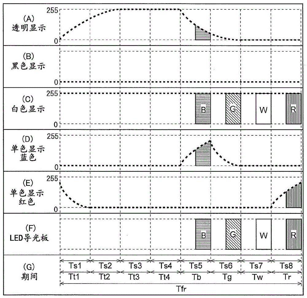
Fig. 8 is a timing chart and a waveform diagram for explaining a display operation of the image display device 1 according to the present embodiment in which the backlight 25 is driven as shown in fig. 5, and fig. 9 is a schematic diagram showing a display example of the image display device 1. The image display device 1 includes a display operation mode in which the backlight 25 is turned on (hereinafter, referred to as "B/L lighting mode") and a display operation mode in which the backlight is not turned on (hereinafter, referred to as "B/L lighting mode"), and fig. 5 and 8 show the display operation of the image display device 1 in the B/L lighting mode. In the present embodiment, the input image data D1 includes control information for specifying which of the B/L lighting mode and the B/L lighting-off mode to operate in, for example, frame units, and the backlight drive circuit 23 receives the lighting control signal Cbl generated by the drive image data calculation unit 33 based on the control information to switch between the B/L lighting mode and the B/L lighting-off mode. However, the following configuration may be adopted: an operation part for switching between a B/L lighting mode and a B/L extinguishing mode is arranged; or a control signal applied to designate any one of the B/L lighting mode and the B/L lighting-off mode is inputted from the outside. Hereinafter, the display operation in the B/L lighting mode will be described with emphasis on the display operation in the B/L lighting mode, and the display operation in the B/L lighting mode will be described later.
In the B/L lighting mode of the present embodiment, as described above, as shown in fig. 5 and 8(F), in the one-frame period Tfr, only the blue light source 27B is in a lit state in the second half of the blue sub-frame period Tb, only the green light source 27g is in a lit state in the second half of the green sub-frame period Tg, all of the red, green, and blue light sources 27r, 27g, and 27B are in a lit state in the second half of the white sub-frame period Tw, only the red light source 27r is in a lit state in the second half of the red sub-frame period Tr, and all of the red, green, and blue light sources 27r, 27g, and 27B are in a lit-off state in the other periods.
In the B/L lighting mode, the driving image data D2 is generated by the driving image data arithmetic unit 33, and the driving image data D2 is used to cause the panel drive circuit 22 to drive the liquid crystal panel 24 as follows. That is, regarding the transparent region of an image to be displayed on the liquid crystal panel 24 (hereinafter, simply referred to as "display image"), in order to form the pixels of the transparent region, pixel data representing a gradation value 255 (maximum transmittance) is written to the liquid crystal panel 24 in the first half (scanning period Tsc) of each of the first to fourth transparent sub-frame periods Tt1 to Tt4 constituting the transparent display sub-frame period Tt, and pixel data representing a gradation value 0 (minimum transmittance) is written to the liquid crystal panel 24 in the first half (scanning period Tsc) of each of the blue, green, white, and red sub-frame periods Tb, Tg, Tw, and Tr constituting the normal display sub-frame period Tn (see fig. 5 and 8 a). Accordingly, in each frame period Tfr, the transmittance of the liquid crystal corresponding to the transparent region changes as indicated by the thick dotted line in fig. 8 (a). In the first to fourth transparent sub-frame periods Tt1 to Tt4, all of the red, green, and blue light sources 27r, 27g, and 27b in the backlight 25 are turned off, and thus the light guide plate 270 is in a transparent state. Therefore, the transparent region in the display image can be seen as a transparent state (a state in which the background is transparently visible).
Regarding a black region in a display image, in order to form the pixels of the black region, pixel data representing a gradation value 0 (minimum transmittance) is also written to the liquid crystal panel 24 in the first half (scanning period Tsc) of an arbitrary subframe period within each frame period Tfr (see fig. 5, fig. 8 (B)). Accordingly, as shown by the thick dotted line in fig. 8B, the transmittance of the liquid crystal corresponding to the black region is constant and is a value (minimum transmittance) corresponding to the gradation value 0 in each frame period Tfr. Thereby, the color of the black region in the display image is seen as black.
Regarding a white area in a display image, in order to form a pixel of the white area, pixel data representing a gradation value 255 (maximum transmittance) is also written to the liquid crystal panel 24 in the first half (scanning period Tsc) of an arbitrary subframe period within each frame period Tfr (see fig. 5, fig. 8 (C)). Accordingly, as shown by the thick dotted line in fig. 8C, the transmittance of the liquid crystal corresponding to the white region is constant in each frame period Tfr, and is a value (maximum transmittance) corresponding to the gradation value 255. In each frame period Tfr, the backlight 25 emits light of a corresponding color in the second half of each of the blue, green, white, and red sub-frame periods Tb, Tg, Tw, and Tr constituting the normal display sub-frame period Tn. By driving the liquid crystal panel 24 and the backlight 25 in this manner, the color of the white region in the display image is seen as white.
When the display image includes a blue single-color region (the gray scale value of the single-color region is set to 255), regarding the single-color region, that is, the blue region, in each frame period Tfr, in the first half of the blue subframe period Tb (scanning period Tsc), pixel data representing a gray scale value 255 (maximum transmittance) is written in the liquid crystal panel 24, and in the first half of the other subframe periods (scanning period Tsc), pixel data representing a gray scale value 0 (minimum transmittance) is written in the liquid crystal panel 24 (refer to fig. 5 and fig. 8 (D)). Accordingly, in each frame period Tfr, the transmittance of the liquid crystal corresponding to the blue region changes as indicated by the thick dotted line in fig. 8 (D). As described above, in the second half of the blue subframe period Tb, only the blue light source 27b is turned on in the backlight 25. By driving the liquid crystal panel 24 and the backlight 25 in this manner, the color of the blue region in the display image is seen as blue.
When the display image includes a monochromatic area of red (the grayscale value of the monochromatic area is made 255), regarding the monochromatic area, that is, the red area, in order to form the pixels of the red area, in each frame period Tfr, pixel data representing a grayscale value 255 (maximum transmittance) is written to the liquid crystal panel 24 in the first half (scanning period Tsc) of the red subframe period Tr, and pixel data representing a grayscale value 0 (minimum transmittance) is written to the liquid crystal panel 24 in the first half (scanning period Tsc) of the other subframe periods (see fig. 5, fig. 8 (E)). Accordingly, in each frame period Tfr, the transmittance of the liquid crystal corresponding to the red region changes as indicated by the thick dotted line in fig. 8 (E). As described above, in the second half of the red subframe period Tr, only the red light source 27r is turned on in the backlight 25. By driving the liquid crystal panel 24 and the backlight 25 in this manner, the color of the red region in the display image is seen as red.
In the B/L lighting mode, by the display operation shown in fig. 8, for example, as shown in fig. 9 a, white display (white display and color display), black display, and transparent display can be simultaneously performed on the same screen.
Fig. 10 is a timing chart and waveform chart for explaining a display operation in the B/L light-off mode of the image display device 1 according to the present embodiment. In the B/L light-off mode, as shown in fig. 10(F), in any period of the sub-frame periods Ts1 to Ts8 in each frame period Tfr, all the light sources 27r, 27g, and 27B of the backlight 25 are in a light-off state, and therefore, neither white display nor color display (including monochrome display) is realized (see fig. 10(C) to (E)).
In the B/L light-off mode, the driving image data D2 is generated by the driving image data arithmetic unit 33, and the driving image data D2 is used to cause the panel drive circuit 22 to drive the liquid crystal panel 24 as follows. That is, regarding the transparent region in the display image, in order to form the pixels of the transparent region, pixel data representing a gradation value 255 (maximum transmittance) is written to the liquid crystal panel 24 in the first half (scanning period Tsc) of an arbitrary subframe period in each frame period Tfr. Accordingly, in each frame period Tfr, as shown in fig. 10 a, the transmittance of the liquid crystal corresponding to the transparent region is constant, and is a value (maximum transmittance) corresponding to the gradation value 255. In addition, the B/L extinction mode light guide plate 270 is maintained in a transparent state. Therefore, the transparent area in the display image is seen as a transparent state.
Regarding the black area in the display image, in order to form the pixels of the black area, pixel data representing a gradation value 0 (minimum transmittance) is written to the liquid crystal panel 24 in the first half (scanning period Tsc) of any subframe period in each frame period Tfr, as in the B/L lighting mode. Accordingly, as shown by the thick dotted line in fig. 10B, the transmittance of the liquid crystal corresponding to the black region is constant and is a value (minimum transmittance) corresponding to the gradation value 0 in each frame period Tfr. Thereby, the color of the black region in the display image is seen as black.
As described above, in the B/L light-off mode, for example, as shown in fig. 9B, black display and transparent display can be simultaneously performed in the same screen, but white display (white display and color display), black display and transparent display cannot be simultaneously performed in the same screen. However, in the B/L light-off mode, in order to form a pixel of a transparent region in a display image, the light guide plate 270 is maintained in a transparent state throughout one frame period Tfr while the transmittance of liquid crystal corresponding to the pixel is maintained at a maximum, and thus the transmittance of the transparent region can be made larger than that of the transparent region in the display image in the B/L light-on mode (see fig. 8(a) and 10 (a)).
<1.3 Effect >
According to the present embodiment as described above, in the B/L lighting mode, the transparent state can be realized in a desired region in the display image by using the time during which the backlight 25 is not lit in the one-frame period Tfr (transparent sub-frame periods Tt1 to Tt4) (see fig. 8(a) and 9 (a)). That is, according to the present embodiment, in the general configuration using the liquid crystal panel and the light guide plate 270, by adopting the above-described driving method based on the field-sequential type, it is possible to simultaneously perform white display, black display, and transparent display in the same screen without complicating the configuration of the display panel and the circuit (simultaneously displaying three states in the same screen). Therefore, conventionally, in order to simultaneously display three states on the same screen, it is not necessary to add a new panel having a structure for forming pixels and a circuit for driving the new panel. Therefore, according to the present embodiment, it is possible to avoid moire fringes and increase in cost due to overlapping of a plurality of panels, and to simultaneously display three states on the same screen.
In addition, in the present embodiment, in each frame period Tfr, since the blue sub-frame period Tb is arranged as the fifth sub-frame period Ts5 immediately after the transparent display sub-frame period Tt (immediately after the fourth transparent sub-frame period Tt4), as shown in fig. 8 a, part of light (blue light) may leak from the blue light source 27b to the front side of the liquid crystal panel 24 in the blue sub-frame period Tb in a transparent region in a displayed image due to the response characteristics of liquid crystal. However, the transmitted light of the polarizing plate used in the liquid crystal panel 24 tends to be yellowish, and since the complementary color of yellow is blue, even if blue light leaks in a transparent region in a display image, a visual discomfort is not easily caused. Therefore, as in the present embodiment, it is preferable to dispose the blue subframe period Tb immediately after the transparent display subframe period Tt. However, when this advantage is particularly noted, the present invention is not limited to the configuration in which the blue subframe period Tb is arranged immediately after the transparent display subframe period Tt.
<1.4 first modification >
Next, a first modification of the first embodiment, in which the driving of the liquid crystal panel 24 is improved to prevent the light source light from leaking in the transparent region in the display image (blue light leakage in the example shown in fig. 8 a), will be described with reference to fig. 5, 11, and 12.
Fig. 11 is a timing chart and a waveform chart for explaining a display operation of the image display device according to the present modification, and fig. 12 is a schematic diagram showing a display example of the image display device according to the present modification. In the configuration of the image display device according to the present modification, the same reference numerals are given to the same or corresponding portions as those of the image display device according to the first embodiment (see fig. 1 to 3). The image display device 1 according to the present modification also includes a B/L lighting mode and a B/L lighting mode, and fig. 5 and 11 show the operation of the image display device 1 according to the present modification in the B/L lighting mode. Hereinafter, the display operation in the B/L lighting mode is written with emphasis on the display operation in the B/L lighting mode, and the display operation in the B/L lighting mode is the same as that in the first embodiment described above, and therefore, the description thereof is omitted (see fig. 10 and fig. 12B).
In the present modification, in order to prevent leakage of light source light (blue light) in the transparent region of the displayed image as much as possible in the blue sub-frame period Tb which is the fifth sub-frame period Ts5, which is a sub-frame period immediately after the transparent display sub-frame period Tt, the driving of the liquid crystal panel 24 in the transparent display sub-frame period Tt (the first to fourth transparent sub-frame periods Tt1 to Tt4) is corrected. The driving of the backlight 25 in the present modification is the same as that in the first embodiment (see fig. 5 and 11F).
In the B/L lighting mode (see fig. 5) of the present modification, the driving image data computing unit 33 generates the driving image data D2, and the driving image data D2 causes the panel driving circuit 22 to drive the liquid crystal panel 24 as follows. That is, regarding the transparent region in the display image, in order to form the pixels of the transparent region, in the first to fourth transparent sub-frame periods Tt1 to Tt4 constituting the transparent display sub-frame period Tt, in the first half (scanning period Tsc) of the first to third transparent sub-frame periods Tt1 to Tt3, pixel data indicating a gradation value 255 (maximum transmittance) is written in the liquid crystal panel 24, similarly to the first embodiment, and in the fourth transparent sub-frame period Tt4, pixel data indicating a gradation value 128 (transmittance of 1/2 having the maximum transmittance) is written in the liquid crystal panel 24, differently from the first embodiment. In the first half (scanning period Tsc) of each of the blue, green, white, and red sub-frame periods Tb, Tg, Tw, and Tr constituting the normal display sub-frame period Tn, pixel data representing a gradation value 0 (minimum transmittance) is written in the liquid crystal panel 24 (see fig. 5 and 11 a), as in the first embodiment described above. Accordingly, in each frame period Tfr, the transmittance of the liquid crystal corresponding to the transparent region changes as indicated by the thick dotted line in fig. 11 (a). This sufficiently suppresses the occurrence of light (blue light) from the blue light source 27b in the bright state in the second half of the blue sub-frame period Tb as the fifth sub-frame period Ts5 in the transparent region.
In the example shown in fig. 11 a, in the fourth transparent sub-frame period Tt4, pixel data indicating a gradation value of 128 (transmittance of 1/2 having the maximum transmittance) is written into the liquid crystal panel 24 for each transparent region, and the gradation value indicated by the pixel data written into the transparent sub-frame period Tt4 immediately before the normal display sub-frame period Tn is not limited to 128, but may be a value that makes the transmittance of the liquid crystal sufficiently small in the second half of the blue sub-frame period Tb that is the sub-frame period Ts5 immediately after the transparent display sub-frame period Tt, that is, in the lighting period of the blue light source 27 b.
In the present modification, by driving the liquid crystal panel 24 as described above, the light source light from the backlight 25 including the blue light source 27B is sufficiently blocked to form a pixel in a transparent region in the B/L lighting mode as shown in fig. 11(a) by adjusting the transmittance of the liquid crystal by utilizing the fact that the backlight 25 is not lit during the transparent display sub-frame period Tt (particularly, the fourth transparent sub-frame period Tt 4).
In the present modification, as shown in fig. 11(B) to (E), the liquid crystal panel 24 for performing black display, white display, and monochrome display is driven in the same manner as in the first embodiment.
According to the present modification as described above, as shown in fig. 12 a, white display (color display), black display, and transparent display can be performed simultaneously on the same screen as in the first embodiment. Further, according to the present modification, as described above, in the case of the transparent display, the light source light from the backlight 25 including the blue light source 27b is sufficiently blocked, and therefore, the transparent display can be performed more favorably than in the first embodiment.
<1.5 second modification >
In the first embodiment, the normal display sub-frame period Tn is constituted by four sub-frame periods including the blue, green, white and red sub-frame periods Tb, Tg, Tw and Tr, but the normal display sub-frame period Tn may be constituted by three sub-frame periods including the blue, green and red sub-frame periods Tb, Tg and Tr without providing the white sub-frame period Tw. Next, an image display device configured as described above will be described as a second modification of the first embodiment with reference to fig. 13 and 14.
Fig. 13 is a timing chart and a waveform chart for explaining a display operation of the image display device according to the present modification, and fig. 14 is a schematic diagram showing a display example of the image display device according to the present modification. In the configuration of the image display device according to the present modification, the same reference numerals are given to the same or corresponding portions as those of the image display device according to the first embodiment (see fig. 1). The image display device 1 according to the present modification also includes a B/L lighting mode and a B/L lighting mode, and fig. 13 shows an operation of the image display device 1 according to the present modification in the B/L lighting mode. Next, the display operation in the B/L lighting mode will be described with emphasis on the display operation, and the display operation in the B/L lighting mode is the same as that in the first embodiment described above, and therefore, the description thereof is omitted (see fig. 10 and 14B).
As shown in fig. 13(F), in the B/L lighting mode of the present modification, in the one-frame period Tfr, only the blue light source 27B is in the on state in the second half of the blue sub-frame period Tb, which is the sixth sub-frame period Ts6, only the green light source 27g is in the on state in the second half of the green sub-frame period Tg, which is the seventh sub-frame period Ts7, only the red light source 27r is in the on state in the second half of the red sub-frame period Tr, which is the eighth sub-frame period Ts8, and all of the red, green, and blue light sources 27r, 27g, and 27B are in the off state in other periods (the first to fifth sub-frame periods Ts1 to Ts5 and the like).
In the B/L lighting mode, the driving image data D2 is generated by the driving image data arithmetic unit 33, and the driving image data D2 is used to cause the panel drive circuit 22 to drive the liquid crystal panel 24 as follows. That is, regarding the transparent region in the display image, in order to form the pixels of the transparent region, pixel data representing a gradation value 255 (maximum transmittance) is written in the liquid crystal panel 24 in the first half (scanning period Tsc) of any cycle of the first to fourth transparent sub-frame periods Tt1 to Tt4 constituting the transparent display sub-frame period Tt, and pixel data representing a gradation value 0 (minimum transmittance) is written in the liquid crystal panel 24 in the first half (scanning period Tsc) of each of the fifth sub-frame period Ts5 (fifth transparent sub-frame period Tt5), the blue sub-frame period Tb, the green sub-frame period Tg, and the red sub-frame period Tr (see fig. 13(a) (G)). Accordingly, in each frame period Tfr, the transmittance of the liquid crystal corresponding to the transparent region changes as indicated by the thick dotted line in fig. 13 (a).
In this modification, the number of sub-frame periods in which the backlight 25 is not lit is increased as compared with the first embodiment, the backlight 25 is also turned off in the fifth sub-frame period Ts5 (fifth transparent sub-frame period Tt5) immediately before the blue sub-frame period Tb, and pixel data representing a gradation value of 0 (minimum transmittance) is written in the liquid crystal panel 24 in the scanning period Tsc which is the first half of the fifth sub-frame period Ts5 as described above with respect to the transparent region in the display image. Therefore, the light guide plate 270 is in the transparent state in the first to fifth sub-frame periods Ts1 to Ts5, and the light source light from the backlight 25 including the blue light source 27b is reliably suppressed from leaking in the transparent region in the normal display sub-frame period Tn including the blue sub-frame period Tb. Accordingly, the transmittance of the transparent region in the display image is improved as compared with the first embodiment.
In the present modification, as shown in fig. 13(B) to (E), the liquid crystal panel 24 for black display, white display, and monochrome display is driven substantially in the same manner as in the first embodiment.
According to the present modification as described above, the white sub-frame period Tw is not provided, and therefore, the effect of preventing color division by the common color sub-frame period cannot be obtained, and the same effect as that of the above-described first embodiment can be obtained except for this. That is, in the present modification, as shown in fig. 14 a, white display (color display), black display, and transparent display may be performed simultaneously on the same screen. Further, according to the present modification, as described above, the transmittance (transmission luminance) of the transparent region in the display image is improved as compared with the first embodiment.
<1.6 third modification >
When a monochrome image of a color of any one light source 27x (x is r, g, or b) of the light sources 27r, 27g, and 27b of the backlight 25 is displayed, that is, when an image (input image) indicated by the input image data D1 is a monochrome image of any one of red, green, and blue, a configuration may be adopted in which only the light source corresponding to the monochrome is turned on (a configuration in which no other light source is used). In this case, the backlight 25 may have only the monochromatic light source 27x, but when the backlight 25 has the red, green, and blue light sources 27r, 27g, and 27b and the lighting control signal Cbl is introduced to instruct which of the red, green, and blue light sources 27r, 27g, and 27b is to be lit, and the image represented by the input image data D1 is a monochromatic image of any of red, green, and blue, it is preferable to generate the driving image data D2, the sub-frame color indication signal BLD, and the lighting control signal Cbl so that the backlight 25 and the liquid crystal panel 24 are appropriately driven in accordance with the monochromatic image. Next, an image display device configured as described above will be described as a third modification of the first embodiment with reference to fig. 15 and 16.
Fig. 15 is a timing chart and a waveform chart for explaining a display operation of the image display device according to the present modification, and fig. 16 is a schematic diagram showing a display example of the image display device according to the present modification. In the configuration of the image display device according to the present modification, the same reference numerals are given to the same or corresponding portions as those of the image display device according to the first embodiment (see fig. 1). The image display device 1 according to the present modification also includes a B/L lighting mode and a B/L lighting mode, and fig. 15 shows an operation of the image display device 1 according to the present modification in the B/L lighting mode. Next, the display operation in the B/L lighting mode will be described with emphasis on the display operation, and the display operation in the B/L lighting mode is the same as that in the first embodiment described above, and therefore, the description thereof is omitted (see fig. 10 and fig. 16B).
The driving image data calculation unit 33 in the present modification determines whether or not the input image is a monochrome image based on the input image data D1, and when determining that the input image is a monochrome image, performs monochrome image determination processing, that is, determines the color of the monochrome image. That is, the monochrome image judgment processing includes the following steps (ST1) to (ST3), and the driving image data calculation unit 33 performs the following processing (image data conversion processing): every time the input image data D1 for one frame is input, the following steps (ST1) to (ST3) are performed, and then the image data D2 for driving is obtained from the input image data D1.
(ST 1): it is determined whether or not the input image represented by the image data D1 for one frame is a monochrome image. Here, the color of each pixel constituting the input image is any one of transparent color, black, red, green, and blue, and when all the pixels of color (any one of red, green, and blue) in the input image are the same color, the input image is determined to be a monochrome image, and it is determined that the input image is not a monochrome image except for this.
(ST 2): when the input image is determined to be a monochrome image in the above step (ST1), it is determined which of red, green, and blue is the color of the color pixel included in the input image (hereinafter, the determined color is referred to as "input color"), and the process proceeds to step ST 3. When the input image is a monochrome image, if a pixel of a color is not included in the input image, the input color is "achromatic color". On the other hand, when it is determined in the above step (ST1) that the input image is not a monochrome image, the lighting control signal Cbl is generated to instruct all of the red light source 27r, the green light source 27g, and the blue light source 27b to be lit, and the monochrome image determination processing is ended.
(ST 3): when the input color is any one of red, green, and blue, the lighting control signal Cbl is generated to instruct only the light source 27 corresponding to the input color among the red light source 27r, the green light source 27g, and the blue light source 27b to light. On the other hand, when the input color is achromatic, the lighting control signal Cbl is generated to instruct all of the red light source 27r, the green light source 27g, and the blue light source 27b to be turned off. Then, the monochrome image determination processing is ended.
On the assumption that all frames of the input image represented by the input image data D1 of the input image display device 1 include pixels of any one of red, blue, and green colors, the processing regarding achromatic colors in the above steps (ST2) and (ST3) is omitted. Next, the above-described assumption is made, and an input image composed of only achromatic pixels can be regarded as a monochrome image.
Fig. 15 is a timing chart and a waveform chart showing a display operation of the image display apparatus 1 when it is determined in the monochrome image determination process that the input color is red, that is, when the image indicated by the input image data D1 is a monochrome image of red. As shown in fig. 15F, in the B/L lighting mode of the present modification, in the one-frame period Tfr, only the red light source 27r is turned on in the second half of the red sub-frame period Tr, which is the eighth sub-frame period Ts8, and in the other periods (the first to seventh sub-frame periods Ts1 to Ts7), the backlight 25 (all of the red, green, and blue light sources 27r, 27B, and 27 g) is turned off.
In the B/L lighting mode, the driving image data D2 is generated by the driving image data arithmetic unit 33, and the driving image data D2 is used to cause the panel drive circuit 22 to drive the liquid crystal panel 24 as follows. That is, regarding the transparent region in the display image, in order to form the pixels of the transparent region, pixel data representing a gradation value 255 (maximum transmittance) is written in the liquid crystal panel 24 in each of the first half (scanning period Tsc) of any period of the first to sixth transparent sub-frame periods Tt1 to Tt6 constituting the transparent display sub-frame period Tt, and pixel data representing a gradation value 0 (minimum transmittance) is written in the liquid crystal panel 24 in each of the first half (scanning period Tsc) of the seventh transparent sub-frame period Tt7 as the seventh sub-frame period Ts7 and the red sub-frame period Tr as the eighth sub-frame period Ts8 (see fig. 15(a) and (G)). Accordingly, in each frame period Tfr, the transmittance of the liquid crystal corresponding to the transparent region changes as indicated by the thick dotted line in fig. 15 (a). As described above, in the first to seventh sub-frame periods Ts1 to Ts7, the light source 27 of the backlight 25 is not turned on, and thus the light guide plate 270 is in a transparent state. Therefore, according to the present modification, the transmittance (transmission luminance) of the transparent region in the display image is further improved.
In the present modification, as shown in fig. 15(E), the liquid crystal panel 24 for monochrome display of red, that is, the liquid crystal panel 2 for forming pixels in a red region in a display image is driven in the same manner as in the first embodiment. As shown in fig. 15(B), the liquid crystal panel 24 for black display is also driven in the same manner as in the first embodiment. In the present modification, since the input image data D1 represents a red monochrome image, it is not necessary to drive the liquid crystal panel 24 for white display and blue monochrome display.
According to the present modification as described above, when the input image data D1 represents a red monochrome image, as shown in fig. 16 a, it is possible to simultaneously perform red monochrome display, black display, and transparent display on the same screen, and further improve the transmittance (through luminance) of the transparent region in the display image of the red monochrome image. Note that, when the input image data D1 represents a monochrome image of another color (any color of blue or green), the backlight 25 and the liquid crystal panel 24 are driven in accordance with the other color as described above (the driving image data D2 and the sub-frame color indication signal BLD for driving as described above are generated by the image data conversion section 10), whereby the same effect can be obtained.
<2 > second embodiment
<2.1 Overall configuration >
Next, an image display device according to a second embodiment will be described. The image display device according to the present embodiment is configured to detect light (hereinafter referred to as "backlight") directed from the outside surface thereof to the back surface of the liquid crystal panel 24, and drive the liquid crystal panel as the light modulation section, taking the backlight into consideration. Fig. 17 is a block diagram showing the configuration of the image display device 1b according to the present embodiment. As in the first embodiment (fig. 1), the image display device 1b includes an image data conversion unit 10 and a display unit 20, the image data conversion unit 10 includes a parameter storage unit 11 and a driving image data calculation unit 33, and the display unit 20 includes: a liquid crystal panel 24 as a light modulation section; a backlight 25 as a light source unit including a red light source 27r, a green light source 27g, a blue light source 27b, and a light guide plate; a timing control circuit 21; a panel drive circuit 22 as a light modulation section drive circuit; a backlight driver circuit 23 as a light source section driver circuit. Since these components in the image display device 1b have substantially the same configurations and functions as those of the image display device 1 in the first embodiment (see fig. 3 and 5), only the configurations and functions different from those in the first embodiment will be described below. In addition to these components, the image display device 1b includes a background light sensor 13 as a photodetector in the image data conversion unit 10, the background light sensor 13 detecting background light, and the background light sensor 13 outputting a sensor signal SD indicating the color and light intensity of the detected background light. The sensor signal SD is input to the driving image data calculation unit 33. In this way, the present embodiment is configured to drive the liquid crystal panel in accordance with a driving method suitable for the backlight (to be described later in detail). In order to apply the driving method to such backlight of the liquid crystal panel, it is preferable to gradually progress so that the change in the time direction is hardly visible. Therefore, when the driving method is gradually applied as described above, the image data conversion unit 10 includes the memory 15, and temporarily stores driving image data for one frame, which takes into account the intensity of the background light indicated by the sensor signal SD and the like, in the memory 15 for gradual application.
The image display device 1b in the present embodiment is also a field-sequential liquid crystal display device, and drives the light sources 27r, 27g, and 27b in the backlight 25 in the same manner (timing) as in the first embodiment (see fig. 3, 5, and fig. 20F described later).
The image display device 1b according to the present embodiment also receives input image data D1, and the input image data D1 includes image data of red, green, blue, and transparent colors. The image data conversion unit 10 acquires the driving image data D2 corresponding to the transparent, green, red, white, and blue sub-frames based on the input image data D1, taking into account the intensity of the background light indicated by the sensor signal SD from the background light sensor 13. The display unit 20 displays transparent, green, red, white, and blue sub-frames in one frame period based on the driving image data D2.
<2.2 summary of characteristic constitution >
Next, an outline of a characteristic configuration of the present embodiment will be described with reference to fig. 18 and 19. Fig. 18 is a diagram for explaining a problem of a conventional image display device to be dealt with by the distinctive feature configuration, and fig. 19 is a diagram for explaining a method of solving the problem in association with the distinctive feature configuration.
Even when the same single color is displayed in a general display device, as shown in fig. 18(a), the displayed single color feels brighter when viewed in a bright room than when viewed in a dark room, according to a contrast effect with the surrounding brightness, i.e., brightness contrast. Therefore, in a bright room, the impression of the monochrome appearance of the display may be poor.
On the other hand, in a transparent display using an organic light emitting diode (hereinafter referred to as "OLED"), a part of a pixel is transparent, and therefore, in a region where a single color is displayed in a display image, a backlight is also transmitted. Therefore, in a bright room, the brightness of the single color of the display may be increased, and the appearance of the single color of the display may be improved. However, when the color of the backlight is different from the monochromatic color of the display, color shift may occur, resulting in deterioration of the impression of the appearance.
In a liquid crystal display device as a field-sequential type transparent display, when a single color corresponding to an arbitrary light source color is displayed, as shown in fig. 18(B), only a light source corresponding to the single color among a plurality of light sources of a backlight is turned on in one sub-frame period in one frame period, and pixel data indicating the maximum transmittance is written in a liquid crystal panel in the sub-frame period, whereby the transmittance of liquid crystal changes as shown by a thick solid line in fig. 18 (B). Therefore, the transmittance of the liquid crystal panel is extremely low in monochrome display, and the luminance of monochrome display is hardly improved in a bright room as compared with a configuration in which a part of the pixels is transparent, such as a transparent display using an OLED. Thus, in a bright room, the impression of the monochrome appearance of the display becomes worse.
In contrast, as in the first embodiment, when the transparent sub-frame period Ttk (sub-frame period in which the light source 27 is not turned on and the light guide plate 270 is in the transparent state) is included in each frame period Tfr in order to simultaneously display three states on the same screen, it is considered that monochrome display can be improved by adjusting the transmittance of the liquid crystal in the transparent sub-frame period Ttk while taking into consideration the color of the backlight and the like. For example, when red should be displayed as a single color, it is considered to drive the liquid crystal panel as follows: when the color of the backlight is white or red, as shown in fig. 19(B), pixel data indicating the maximum transmittance is written to the liquid crystal panel not only in the sub-frame period Tr in which the red light source is turned on but also in any cycle of the transparent sub-frame period Ttk in which the backlight is not turned on. With the above configuration, as shown in fig. 19(a), in a bright room, the impression of the appearance of monochromatic red as the display can be improved. As a distinctive configuration using the above-described backlight sensor 13, the image display device 1b according to the present embodiment has such a configuration. However, the color of the background light is white, and the image display device 1b in the present embodiment is configured to improve monochrome display based on the intensity (brightness) of the background light of the color and intensity indicated by the sensor signal SD. Therefore, in the present embodiment, a photodetector that detects only the intensity of the background light may be used as the background light sensor 13. Note that, a configuration for improving monochrome display using a color (background color) indicated by the sensor signal SD will be described later as a modification of the present embodiment.
<2.3 display action >
Fig. 20 is a timing chart and a waveform chart for explaining a display operation of the image display device 1b in the present embodiment, and fig. 21 is a schematic diagram showing a display example of the image display device 1 b. As in the first embodiment, the image display device 1B of the present embodiment includes a B/L lighting mode and a B/L lighting-off mode, and fig. 20 and 21(a) show the operation of the image display device 1B in the B/L lighting mode. Next, the display operation in the B/L lighting-on mode will be described with emphasis on the display operation, and the display operation in the B/L lighting-off mode is the same as that in the first embodiment described above, and therefore, the description thereof is omitted (see fig. 10 and fig. 21B).
The driving image data arithmetic unit 33 in the image display device 1b generates the driving image data D2 to receive the input image data D1 from the outside and the sensor signal SD from the background light sensor 13, and adjusts the gradation (the transmittance of the liquid crystal) in at least one of the transparent sub-frame periods Tt (the first to fourth transparent sub-frame periods Tt1 to Tt4) in accordance with the intensity of the background light based on the sensor signal SD, thereby improving the luminance of the monochrome display by the background light. Specifically, the following display operation is performed.
In the B/L lighting mode of the present embodiment (see fig. 5), particularly when monochrome display of a color corresponding to a display color sub-frame period (in the example shown in fig. 20, blue sub-frame period Tb and red sub-frame period Tr) adjacent to the transparent display sub-frame period Tt (first to fourth transparent sub-frame periods Tt1 to Tt4) is performed, the liquid crystal panel 24 is driven as follows: the gray scales (corresponding to the transmittance of liquid crystal) in the first to fourth transparent sub-frame periods Tt1 to Tt4, which are periods when the light source 27 is not lit and the light guide plate 270 is in the transparent state, are adjusted, whereby bright display is obtained by using white background light.
That is, when the image (input image) represented by the input image data D1 includes pixels of the light source color (blue) in the blue sub-frame period Tb as the fifth sub-frame period Ts5, in order to increase the luminance of the blue region in the display image, the gradation of the pixels in the blue region is adjusted in at least one of the first to fourth transparent sub-frame periods Tt1 to Tt 4. At this time, the driving image data D2 is generated from the input image data D1 by the driving image data arithmetic unit 33 taking into account the intensity of the background light indicated by the sensor signal SD, and the liquid crystal panel 24 is driven by the panel drive circuit 22 using the driving image data D2, so that the luminance of the pixels in the blue region is preferentially increased. More specifically, the image data for driving D2 is generated as follows: the larger the intensity of the background light is, the larger the gradation of the pixels in the blue region becomes in at least one of the first to fourth transparent sub-frame periods Tt1 to Tt 4. Accordingly, the greater the intensity of the background light, the greater the total gradation value (transmittance of liquid crystal) of the pixels in the blue region, that is, the integrated value or the average value of the gradation values of the pixels in the periods Tt1 to Tt4, in the first to fourth transparent sub-frame periods Tt1 to Tt 4. For example, as shown in fig. 20(D), in the first half (scanning period Tsc) of each of the first to third transparent sub-frame periods Tt1 to Tt3, pixel data indicating a gradation value 0 (minimum transmittance) is written into the liquid crystal panel 24, but in the first half (scanning period Tsc) of each of the fourth sub-frame period Tt4, pixel data indicating a gradation value 255 (maximum transmittance) is written into the liquid crystal panel 24 as well as the fifth sub-frame period Ts5 (blue sub-frame period Tb). Accordingly, in each frame period Tfr, the transmittance of the liquid crystal corresponding to the blue region changes as indicated by the thick broken line in fig. 20(D), and the luminance of the blue region in the display image is increased by using the background light in the fourth sub-frame period Tt4 and increasing the transmittance of the liquid crystal in the blue sub-frame period Tb. In the example shown in fig. 20D, the transmittance of the liquid crystal in the fourth sub-frame period Tt4 (the transparent sub-frame period immediately before the blue sub-frame period Tb) is increased, and thus the display luminance can be increased by increasing the transmittance in the blue sub-frame period Tb.
In addition, when the light source color (red) of the red sub-frame period Tr, which is the eighth sub-frame period Ts8, is included in the input image, the gray scale of the pixels of the red region is adjusted in at least one of the first to fourth transparent sub-frame periods Tt1 to Tt4 to increase the luminance of the red region in the display image. At this time, the driving image data computing unit 33 generates the driving image data D2 from the input image data D1, taking into account the intensity of the background light indicated by the sensor signal SD, and the panel driving circuit 22 drives the liquid crystal panel 24 using the driving image data D2, thereby preferentially increasing the luminance of the pixels in the red region. More specifically, the image data for driving D2 is generated as follows: as the intensity of the background light increases, the gradation of the pixels in the red region increases in at least one of the first to fourth transparent sub-frame periods Tt1 to Tt 4. Accordingly, the greater the intensity of the background light, the greater the total gradation value (transmittance of liquid crystal) of the pixels of the red region, that is, the integrated value or the average value of the gradation values of the pixels in the periods Tt1 to Tt4, in the first to fourth transparent sub-frame periods Tt1 to Tt 4. For example, as shown in fig. 20E, in the first half (scanning period Tsc) of the red subframe period Tr as the eighth subframe period Ts8, pixel data indicating a gradation value 255 (maximum transmittance) is written in the liquid crystal panel 24, in the next frame period Tfr, in the first half (scanning period Tsc) of the first transparent subframe period Tt1 adjacent to the red subframe period Tr, pixel data indicating a gradation value 128 (transmittance of 1/2 of the maximum transmittance) is written in the liquid crystal panel 24, and in the scanning period Tsc of the other periods including the third and fourth transparent subframe periods Tt3, Tt4, pixel data indicating a gradation value 0 (minimum transmittance) is written in the liquid crystal panel 24. Note that, when the intensity of the background light indicated by the sensor signal SD is larger, in order to display the red region (red image) more brightly, for example, pixel data indicating a gradation value 255 (maximum transmittance) may be written into the liquid crystal panel 24 in the first half (scanning period Tsc) of each of the first to fourth transparent sub-frame periods Tt1 to Tt4 instead of the driving shown in fig. 20E.
In the present embodiment, as shown in fig. 20(B) and (C), the liquid crystal panel 24 for black display and white display is driven in the same manner as in the first embodiment.
<2.4 Effect >
According to the present embodiment described above, in addition to the effects of the first embodiment described above, the following effects can be obtained. That is, in order to utilize the background light in at least one of the first to fourth transparent sub-frame periods Tt1 to Tt4 and to increase the transmittance of the liquid crystal in the blue sub-frame period Tb, the gray scale of the pixel in the blue region is adjusted in at least one of the first to fourth transparent sub-frame periods Tt1 to Tt4, taking into account the intensity of the background light indicated by the sensor signal SD (see fig. 20 (D)). Thereby, a blue region (blue image) in the display image can be displayed brightly. Thus, the visibility of the blue region in the display image can be maintained well even in an environment where the surroundings are bright.
In addition, in order to utilize the background light in at least one of the first to fourth transparent sub-frame periods Tt1 to Tt4 and to increase the transmittance of the liquid crystal in the red sub-frame period Tr, the gradation of the pixels in the red region is adjusted in at least one of the first to fourth transparent sub-frame periods Tt1 to Tt4, taking into account the intensity of the background light indicated by the sensor signal SD (see fig. 20 (E)). This makes it possible to brightly display a red region (red image) in the display image. Accordingly, the visibility of the red region in the display image can be maintained well even in an environment where the surroundings are bright.
Note that even when a pixel of a light source color (green) other than blue and red is included in the input image, the gray scale of the pixel of the light source color can be adjusted by taking the intensity of the background light indicated by the sensor signal SD into consideration in at least one of the first to fourth transparent sub-frame periods Tt1 to Tt4, thereby increasing the luminance of the same region of the color as the light source color in the display image. In addition, in the present embodiment, since the color of the background light is white, even when the input image includes a pixel of an arbitrary color based on a plurality of primary colors (in the present embodiment, three primary colors consisting of red, blue, and green), the luminance of a region of the arbitrary color in the display image can be increased by adjusting the gray scale of the pixel of the arbitrary color in consideration of the intensity of the background light indicated by the sensor signal SD in at least one of the first to fourth transparent sub-frame periods Tt1 to Tt 4.
<2.5 first modification >
In the second embodiment described above, the color of the background light is made white, but even in the case where the color of the background light is not white, the same effect as that of the second embodiment described above can be obtained if it is close to the color of the monochrome display to be increased in luminance. In contrast, when the color of the backlight is not a color close to the color of the monochrome display to be brightened, the actual display color may appear to be deviated from the original chromaticity in the monochrome display region. Even in such a case, similarly to the second embodiment, in at least one of the first to fourth transparent sub-frame periods Tt1 to Tt4, the luminance of the region having the same color as the light source color is increased by adjusting the gradation of the pixel of the light source color in consideration of the intensity of the background light indicated by the sensor signal SD, whereby a decrease in visibility (a phenomenon of appearing dark in a bright environment) can be suppressed in a bright environment. However, when the color of the backlight is not a color close to that of the monochrome display to be enhanced in luminance, it is more preferable to drive the liquid crystal panel in a form different from that when the color of the backlight is close to that of white or monochrome display in order to suppress the actual display color from deviating from the original chromaticity. Next, an image display device having such a configuration will be described as a first modification of the second embodiment. In the following description, the display operation in the B/L lighting mode is mainly described, and the display operation in the B/L lighting mode is the same as that in the first embodiment, and therefore, the description thereof is omitted (see fig. 10 and 21B).
The image display device according to the present modification is configured as shown in fig. 17, similarly to the second embodiment. Next, of the constituent members of the image display device in the present modification, the same or corresponding constituent members as those shown in fig. 17 are given the same reference numerals. In the present modification, the driving image data calculation unit 33 performs a background color determination process of determining whether or not the color of the background light (background color) indicated by the sensor signal SD is a color close to the color of the monochrome display to be enhanced in luminance (for example, simply determining whether or not the background color is white or the same color as the color of the monochrome display), and generates the driving image data D2 based on the determination result. Next, the display operation of the present modification will be described with reference to fig. 8, 20 and the like, focusing on the details of the driving based on the background color determination process. In the present modification, the driving image data D2 is generated, and the driving image data D2 is driven as described below based on the background color determination process.
That is, when it is determined that the background color indicated by the sensor signal SD is close to the light source color (blue) of the blue sub-frame period Tb as the fifth sub-frame period Ts5, the liquid crystal panel 24 is driven as in the second embodiment described above with respect to the pixels of the blue region in the display image (see fig. 20(D)), and when it is determined that the background color indicated by the sensor signal SD is close to the light source color (red) of the red sub-frame period Tr as the eighth sub-frame period Ts8, the liquid crystal panel 24 is driven as in the second embodiment described above with respect to the pixels of the red region in the display image (see fig. 20 (E)). On the other hand, when it is determined that the background color indicated by the sensor signal SD is not close to the light source color (blue) of the blue sub-frame period Tb, the liquid crystal panel 24 is driven so as to suppress a shift in display color due to the background color with respect to the pixels in the blue region in the display image, for example, the liquid crystal panel 24 is driven as shown in fig. 8 (D). When it is determined that the background color indicated by the sensor signal SD is not close to the light source color (red) in the red sub-frame period Tr, the liquid crystal panel 24 is driven so as to suppress a shift in display color due to the background color with respect to the pixels in the red region in the display image, for example, the liquid crystal panel 24 is driven as shown in fig. 8E.
According to the present modification as described above, it is possible to suppress the display color from shifting from the original chromaticity due to the background light, and at the same time, when the background color indicated by the sensor signal SD is close to the color of the monochrome display whose luminance is to be increased, the same effect as that of the above-described second embodiment can be obtained.
<2.6 second modification >
Next, on the premise that an image is displayed (an image composed of a monochromatic region and a transparent region is displayed) in a monochromatic color that is the color of any one of the light sources 27r, 27g, and 27b of the backlight 25, referring to fig. 3, 17, 22, and 23, an image display device in which the gradation (the transmittance of liquid crystal) is adjusted in a transparent sub-frame period in which the light source 27 of the backlight 25 is not lit and the light guide plate 270 is transparent, thereby further improving monochromatic display will be described as a second modification of the second embodiment.
The driving image data arithmetic unit 33 in the present modification performs a monochrome image determination process of determining whether or not the input image is a monochrome image based on the input image data D1, and when it is determined that the input image is a monochrome image, determining the color of the monochrome image. Similarly to the monochrome image determination processing in the third modification of the first embodiment, the monochrome image determination processing includes the above-described steps (ST1) to (ST3), and the driving image data calculation unit 33 performs processing (image data conversion processing) such that the steps (ST1) to (ST3) are executed every time the input image data D1 for one frame is input, and then the driving image data D2 is obtained from the input image data D1.
Fig. 22 is a timing chart and a waveform chart for explaining a display operation of the image display device according to the present modification, and fig. 23 is a schematic diagram showing a display example of the image display device according to the present modification. In the configuration of the image display device according to the present modification, the same reference numerals are given to the same or corresponding portions as those of the image display device according to the second embodiment (see fig. 3 and 17). Further, the image display device 1B in the present modification also includes a B/L lighting mode and a B/L lighting mode, and fig. 22 shows an operation of the image display device 1B in the B/L lighting mode in the present modification. Next, the display operation in the B/L lighting mode will be described with emphasis on the display operation, and the display operation in the B/L lighting mode is the same as in the first and second embodiments described above, and therefore, the description thereof is omitted (see fig. 10 and fig. 23B). In the following, similarly to the second embodiment, the color of the background light is white, and the image display device 1b in the present modification is configured to improve monochrome display based on the intensity (luminance) of the color and intensity of the background light indicated by the sensor signal SD. Therefore, in the present modification, a photodetector that detects only the intensity of the background light may be used as the background light sensor 13. In the following, a description will be given of a display operation when the input image data D1 represents a red monochrome image, and a description will be omitted since a display operation when a monochrome image of any of the other light source colors, i.e., blue, green, and white, is represented can be grasped from the following description.
Fig. 22 is a timing chart and a waveform chart showing a display operation of the image display device 1b when the monochrome image determination process described above determines that the input color is red, that is, when the image indicated by the input image data D1 is a monochrome image of red. As shown in fig. 22F, in the B/L lighting mode of the present modification, in the one-frame period Tfr, only the red light source 27r is turned on in the second half of the red sub-frame period Tr, which is the eighth sub-frame period Ts8, and in other periods (the first to seventh sub-frame periods Ts1 to Ts7 and the like), the backlight 25 (all of the red, green, and blue light sources 27r, 27g, and 27B) is turned off. Thus, the first to seventh sub-frame periods Ts1 to Ts7 are also referred to as first to seventh transparent sub-frame periods Tt1 to Tt7, respectively.
As shown in fig. 17, the driving image data arithmetic unit 33 in the image display device 1b generates the driving image data D2 to receive the input image data D1 from the outside and the sensor signal SD from the background light sensor 13, and adjusts the gradation (the transmittance of the liquid crystal) in at least one of the transparent sub-frame periods Tt (the first to fourth transparent sub-frame periods Tt1 to Tt4) in accordance with the intensity of the background light based on the sensor signal SD, thereby improving the luminance of the monochrome display by the background light. Specifically, the following display operation is performed.
That is, when the image represented by the input image data D1 is a red monochrome image, the gray scale is adjusted so that the transmittance of the liquid crystal is maximized in the first to seventh transparent sub-frame periods Tt1 to Tt7, which are the first to seventh sub-frame periods Ts1 to Ts7, in accordance with the intensity of the background light indicated by the sensor signal SD, so that the luminance of the red region in the display image is increased. At this time, the driving image data D2 is generated from the input image data D1 by the driving image data arithmetic unit 33 taking into account the intensity of the background light indicated by the sensor signal SD, and the liquid crystal panel 24 is driven by the panel drive circuit 22 using the driving image data D2, so that the luminance of the pixels in the red region is preferentially increased. More specifically, the image data for driving D2 is generated as follows: as the intensity of the background light increases, the gradation of the pixels in the red region increases in at least one of the first to fourth transparent sub-frame periods Tt1 to Tt 4. Accordingly, the greater the intensity of the background light, the greater the total gradation value (transmittance of liquid crystal) of the pixels in the red region, that is, the integrated value or the average value of the gradation values of the pixels in the periods Tt1 to Tt4, in the first to fourth transparent sub-frame periods Tt1 to Tt 4. For example, as shown in fig. 22E, not only in the first half (scanning period Tsc) of the red sub-frame period Tr, which is the eighth sub-frame period Ts8, pixel data indicating a gradation value 255 (maximum transmittance) is written in the liquid crystal panel 24, but also in the first half (scanning period Tsc) of each of the first to seventh transparent sub-frame periods Tt1 to Tt7, which are the first to seventh sub-frame periods Ts1 to Ts7, pixel data indicating a gradation value 255 (maximum transmittance) is written in the liquid crystal panel 24. Since only the red light source 27r of the light sources 27r, 27g, and 27b of the backlight 25 emits light and the background color is white, color mixing does not occur even when the liquid crystal panel 24 is driven in this manner.
In the present modification, even if the input image is a monochrome image of blue or green (even if the monochrome image determination processing determines that the input color is blue or green), a display operation corresponding to the input color is performed, and the display operation is the same as the above-described display operation.
According to the present modification as described above, when the input image is a monochrome image, the gray scale of the region of the input color (in the example of fig. 22, the red region) in the display image is adjusted in at least one of the first to seventh transparent sub-frame periods Tt1 to Tt7 so that the transmittance of the liquid crystal in the primary color sub-frame period (in the example of fig. 22, the red sub-frame period Tr) corresponding to the input color, which is the color of the monochrome image, is maximally increased according to the intensity of the background light, whereby the region of the input color (in the example of fig. 22, the red region (red image)) in the display image can be brightly displayed. For example, in accordance with the intensity of the background light, the transmittance of the liquid crystal in the region of the input color is maximized, for example, in the first to seventh transparent sub-frame periods Tt1 to Tt7, and the gradation of the region of the input color is adjusted in such a manner. This makes it possible to more brightly display the region of the input color in the display image (in the example of fig. 22, this region is a red region). Accordingly, even in an environment where the surroundings are bright, the visibility of the region of the input color (in the example of fig. 22, the red region) in the display image can be maintained well.
As in the first modification of the second embodiment, the present modification is modified such that the driving image data D2 is generated based on the background color determination process using the color (background color) indicated by the sensor signal SD. By the correction as described above, it is possible to suppress the background light from causing the display color to shift from the original chromaticity, and at the same time, when the background color shown by the sensor signal SD is close to the color of the monochrome image whose luminance is to be improved, the same effect as that of the present modification can be obtained.
<3 > other modifications
The present invention is not limited to the above embodiments and the above modifications, and various modifications may be made without departing from the scope of the present invention.
In the above embodiments, the display color subframe periods are arranged in the order of the blue subframe period Tb, the green subframe period Tg, the white subframe period Tw, and the blue subframe period Tb in the normal display subframe period Tn (see fig. 5, 8F, and 20F), but the arrangement order is not limited to the arrangement order in the above embodiments. In each of the above embodiments, the normal display sub-frame period Tn is constituted by the blue, green, and red sub-frame periods Tb, Tg, and Tb, and may be constituted by sub-frame periods of other primary colors and a common color sub-frame period.
In each of the above embodiments and modifications thereof, the image display device includes a B/L lighting mode and a B/L lighting-off mode (see fig. 8 to 10, etc.), and may be configured to perform only the operation in the B/L lighting mode.
In each of the above embodiments and the modifications thereof, the backlight 25 as the light source portion of the image display device is an edge light type backlight including the light guide plate 270, and the light guide plate 270 emits light from the light sources 27r, 27g, and 27b such as LEDs incident from the side surface from the main surface (fig. 2). For example, a planar lighting device may be used as the light source unit, the planar lighting device being configured such that a plurality of elements such as organic EL elements (OLEDs) are arranged in a two-dimensional shape, and the planar lighting device is in a transparent state when the plurality of elements are in a light-off state.
Note that, although the image display devices in the respective embodiments and the modifications thereof have been described above, the image display devices in the various modifications may be configured by arbitrarily combining the features of the image display devices in the embodiments and the modifications thereof as long as the properties thereof are not violated.
Description of the reference numerals
1.1 b … image display device
10 … image data conversion part
20 … display part
11 … parameter storage part
13 … background light sensor
33 … driving image data arithmetic unit
21 … timing control circuit
22 … Panel driver Circuit (light modulation part driver Circuit)
23 … backlight drive circuit (light source drive circuit)
24 … liquid crystal panel (light modulation part)
25 … backlight (light source)
26 … pixel
27 … light source
27r … Red light Source
27g … Green light Source
27b … blue light source
CswR … red light source control signal
Cwg … green light source control signal
CswB … blue light source control signal
SD … sensor signal
Tfr … frame period
Tt … transparent display sub-frame period
Tn … Normal display sub-frame period
Ttk … transparent sub-frame period (k 1, 2 …)
Tb … blue subframe period
Tg … Green subframe period
Tr … Red subframe period
Tw … white subframe period