CN109727952B - Interconnection pattern structure, semiconductor structure and manufacturing method thereof - Google Patents
Interconnection pattern structure, semiconductor structure and manufacturing method thereof Download PDFInfo
- Publication number
- CN109727952B CN109727952B CN201810926996.7A CN201810926996A CN109727952B CN 109727952 B CN109727952 B CN 109727952B CN 201810926996 A CN201810926996 A CN 201810926996A CN 109727952 B CN109727952 B CN 109727952B
- Authority
- CN
- China
- Prior art keywords
- metal layer
- metal
- dielectric member
- dielectric
- layer
- Prior art date
- Legal status (The legal status is an assumption and is not a legal conclusion. Google has not performed a legal analysis and makes no representation as to the accuracy of the status listed.)
- Active
Links
Images


Classifications
-
- H—ELECTRICITY
- H10—SEMICONDUCTOR DEVICES; ELECTRIC SOLID-STATE DEVICES NOT OTHERWISE PROVIDED FOR
- H10W—GENERIC PACKAGES, INTERCONNECTIONS, CONNECTORS OR OTHER CONSTRUCTIONAL DETAILS OF DEVICES COVERED BY CLASS H10
- H10W20/00—Interconnections in chips, wafers or substrates
- H10W20/01—Manufacture or treatment
- H10W20/031—Manufacture or treatment of conductive parts of the interconnections
- H10W20/056—Manufacture or treatment of conductive parts of the interconnections by filling conductive material into holes, grooves or trenches
-
- H—ELECTRICITY
- H10—SEMICONDUCTOR DEVICES; ELECTRIC SOLID-STATE DEVICES NOT OTHERWISE PROVIDED FOR
- H10W—GENERIC PACKAGES, INTERCONNECTIONS, CONNECTORS OR OTHER CONSTRUCTIONAL DETAILS OF DEVICES COVERED BY CLASS H10
- H10W20/00—Interconnections in chips, wafers or substrates
- H10W20/20—Interconnections within wafers or substrates, e.g. through-silicon vias [TSV]
-
- H—ELECTRICITY
- H10—SEMICONDUCTOR DEVICES; ELECTRIC SOLID-STATE DEVICES NOT OTHERWISE PROVIDED FOR
- H10P—GENERIC PROCESSES OR APPARATUS FOR THE MANUFACTURE OR TREATMENT OF DEVICES COVERED BY CLASS H10
- H10P14/00—Formation of materials, e.g. in the shape of layers or pillars
- H10P14/40—Formation of materials, e.g. in the shape of layers or pillars of conductive or resistive materials
-
- H—ELECTRICITY
- H10—SEMICONDUCTOR DEVICES; ELECTRIC SOLID-STATE DEVICES NOT OTHERWISE PROVIDED FOR
- H10W—GENERIC PACKAGES, INTERCONNECTIONS, CONNECTORS OR OTHER CONSTRUCTIONAL DETAILS OF DEVICES COVERED BY CLASS H10
- H10W20/00—Interconnections in chips, wafers or substrates
- H10W20/01—Manufacture or treatment
- H10W20/021—Manufacture or treatment of interconnections within wafers or substrates
- H10W20/023—Manufacture or treatment of interconnections within wafers or substrates the interconnections being through-semiconductor vias
- H10W20/0234—Manufacture or treatment of interconnections within wafers or substrates the interconnections being through-semiconductor vias comprising etching via holes that stop on pads or on electrodes
-
- H—ELECTRICITY
- H10—SEMICONDUCTOR DEVICES; ELECTRIC SOLID-STATE DEVICES NOT OTHERWISE PROVIDED FOR
- H10W—GENERIC PACKAGES, INTERCONNECTIONS, CONNECTORS OR OTHER CONSTRUCTIONAL DETAILS OF DEVICES COVERED BY CLASS H10
- H10W20/00—Interconnections in chips, wafers or substrates
- H10W20/01—Manufacture or treatment
- H10W20/021—Manufacture or treatment of interconnections within wafers or substrates
- H10W20/023—Manufacture or treatment of interconnections within wafers or substrates the interconnections being through-semiconductor vias
- H10W20/0242—Manufacture or treatment of interconnections within wafers or substrates the interconnections being through-semiconductor vias comprising etching via holes from the back sides of the chips, wafers or substrates
-
- H—ELECTRICITY
- H10—SEMICONDUCTOR DEVICES; ELECTRIC SOLID-STATE DEVICES NOT OTHERWISE PROVIDED FOR
- H10W—GENERIC PACKAGES, INTERCONNECTIONS, CONNECTORS OR OTHER CONSTRUCTIONAL DETAILS OF DEVICES COVERED BY CLASS H10
- H10W20/00—Interconnections in chips, wafers or substrates
- H10W20/01—Manufacture or treatment
- H10W20/031—Manufacture or treatment of conductive parts of the interconnections
- H10W20/032—Manufacture or treatment of conductive parts of the interconnections of conductive barrier, adhesion or liner layers
- H10W20/038—Manufacture or treatment of conductive parts of the interconnections of conductive barrier, adhesion or liner layers covering conductive structures
-
- H—ELECTRICITY
- H10—SEMICONDUCTOR DEVICES; ELECTRIC SOLID-STATE DEVICES NOT OTHERWISE PROVIDED FOR
- H10W—GENERIC PACKAGES, INTERCONNECTIONS, CONNECTORS OR OTHER CONSTRUCTIONAL DETAILS OF DEVICES COVERED BY CLASS H10
- H10W20/00—Interconnections in chips, wafers or substrates
- H10W20/01—Manufacture or treatment
- H10W20/031—Manufacture or treatment of conductive parts of the interconnections
- H10W20/069—Manufacture or treatment of conductive parts of the interconnections by forming self-aligned vias or self-aligned contact plugs
-
- H—ELECTRICITY
- H10—SEMICONDUCTOR DEVICES; ELECTRIC SOLID-STATE DEVICES NOT OTHERWISE PROVIDED FOR
- H10W—GENERIC PACKAGES, INTERCONNECTIONS, CONNECTORS OR OTHER CONSTRUCTIONAL DETAILS OF DEVICES COVERED BY CLASS H10
- H10W20/00—Interconnections in chips, wafers or substrates
- H10W20/01—Manufacture or treatment
- H10W20/031—Manufacture or treatment of conductive parts of the interconnections
- H10W20/0698—Local interconnections
-
- H—ELECTRICITY
- H10—SEMICONDUCTOR DEVICES; ELECTRIC SOLID-STATE DEVICES NOT OTHERWISE PROVIDED FOR
- H10W—GENERIC PACKAGES, INTERCONNECTIONS, CONNECTORS OR OTHER CONSTRUCTIONAL DETAILS OF DEVICES COVERED BY CLASS H10
- H10W20/00—Interconnections in chips, wafers or substrates
- H10W20/40—Interconnections external to wafers or substrates, e.g. back-end-of-line [BEOL] metallisations or vias connecting to gate electrodes
-
- H—ELECTRICITY
- H10—SEMICONDUCTOR DEVICES; ELECTRIC SOLID-STATE DEVICES NOT OTHERWISE PROVIDED FOR
- H10W—GENERIC PACKAGES, INTERCONNECTIONS, CONNECTORS OR OTHER CONSTRUCTIONAL DETAILS OF DEVICES COVERED BY CLASS H10
- H10W70/00—Package substrates; Interposers; Redistribution layers [RDL]
- H10W70/01—Manufacture or treatment
- H10W70/05—Manufacture or treatment of insulating or insulated package substrates, or of interposers, or of redistribution layers
- H10W70/095—Manufacture or treatment of insulating or insulated package substrates, or of interposers, or of redistribution layers of vias therein
Landscapes
- Internal Circuitry In Semiconductor Integrated Circuit Devices (AREA)
Abstract
本发明实施例涉及一种互连图案结构、半导体结构及其制造方法。半导体结构包含:半导体衬底,其具有有源侧;互连层,其位于所述半导体衬底的所述有源侧上方;及贯穿衬底导通孔TSV,其从所述半导体衬底延伸到第一金属层。所述互连层包含最靠近所述半导体衬底的所述有源侧的第一金属层,所述第一金属层的厚度低于1微米,且从俯视视角看,所述第一金属层的连续金属构件的尺寸小于2微米。所述连续金属构件由第一介电构件切断。

Embodiments of the present invention relate to an interconnection pattern structure, a semiconductor structure and a manufacturing method thereof. A semiconductor structure comprising: a semiconductor substrate having an active side; an interconnect layer over the active side of the semiconductor substrate; and a through substrate via TSV extending from the semiconductor substrate to the first metal layer. The interconnection layer includes a first metal layer closest to the active side of the semiconductor substrate, the thickness of the first metal layer is less than 1 micron, and from a top view, the first metal layer The size of the continuous metal member is less than 2 microns. The continuous metal member is severed by the first dielectric member.
Description
技术领域technical field
本发明实施例涉及互连图案结构、半导体结构及其制造方法。Embodiments of the present invention relate to an interconnection pattern structure, a semiconductor structure and a manufacturing method thereof.
背景技术Background technique
半导体集成电路(IC)工业已经历快速成长。IC材料及设计的技术进步已产生数代IC,其中各代具有比前一代更小及更复杂的电路。然而,这些进步已增加处理及制造IC的复杂性,且为实现这些进步,需要IC处理及制造的类似发展。在集成电路演进的过程中,功能密度(即,单位芯片面积的互连装置的数目)已普遍增大,同时几何大小(即,可使用工艺产生的最小组件(或线))已减小。The semiconductor integrated circuit (IC) industry has experienced rapid growth. Technological advances in IC materials and design have produced generations of ICs, each generation having smaller and more complex circuits than the previous generation. However, these advances have increased the complexity of handling and manufacturing ICs, and similar developments in IC processing and manufacturing are required to achieve these advances. In the course of integrated circuit evolution, functional density (ie, the number of interconnected devices per chip area) has generally increased while geometry size (ie, the smallest component (or line) that can be produced using a process) has decreased.
作为半导体制造的一部分,可形成导电元件以对一IC的各种组件提供电互连。例如,可通过在层间介电质(ILD)中蚀刻开口且使用导电材料填充开口来形成用于使不同金属层互连的导电导通孔。然而,随着半导体制造技术节点不断演进,临界尺寸及节距变得越来越小,且处理窗变得越来越严紧。因此,会发生重叠误差(例如失准导通孔),其可导致例如可靠性测试边限减小或制造性能变差的问题。As part of semiconductor fabrication, conductive elements may be formed to provide electrical interconnection to various components of an IC. For example, conductive vias for interconnecting different metal layers may be formed by etching openings in an interlayer dielectric (ILD) and filling the openings with a conductive material. However, as semiconductor manufacturing technology nodes continue to evolve, critical dimensions and pitches become smaller and smaller, and processing windows become tighter. As a result, overlay errors (such as misaligned vias) occur, which can lead to problems such as reduced reliability test margins or poor manufacturing performance.
因此,尽管常规导通孔形成过程一般已足以满足其所希望目的,但其尚无法在各方面令人满意。Thus, while conventional via formation processes have generally been adequate for their intended purposes, they have not been satisfactory in all respects.
发明内容Contents of the invention
本发明的一实施例揭露一种半导体结构,其包括:半导体衬底,其具有有源侧;互连层,其接近所述半导体衬底的所述有源侧,所述互连层包括最靠近所述半导体衬底的所述有源侧的第一金属层,所述第一金属层的厚度小于1微米,且从俯视视角看,所述第一金属层的连续金属构件的尺寸小于2微米,其中所述连续金属构件由第一介电构件切断;贯穿衬底导通孔(TSV),其从所述半导体衬底延伸到所述第一金属层。An embodiment of the present invention discloses a semiconductor structure, which includes: a semiconductor substrate, which has an active side; an interconnection layer, which is close to the active side of the semiconductor substrate, and the interconnection layer includes the most The first metal layer close to the active side of the semiconductor substrate, the thickness of the first metal layer is less than 1 micron, and the size of the continuous metal member of the first metal layer is less than 2 microns, wherein the continuous metal member is severed by a first dielectric member; a through substrate via (TSV) extending from the semiconductor substrate to the first metal layer.
本发明的一实施例揭露一种互连图案结构,其包括:第一金属层,从俯视视角看,所述第一金属层的连续金属构件的尺寸小于2微米,其中所述连续金属构件由第一介电构件切断;及第二金属层,其位于所述第一金属层上方,从俯视视角看,所述第二金属层的连续金属构件的尺寸小于2微米,其中所述连续金属构件由第二介电构件切断,其中所述第二介电构件安置成与所述第一介电构件错开。An embodiment of the present invention discloses an interconnection pattern structure, which includes: a first metal layer, the size of the continuous metal member of the first metal layer is less than 2 micrometers when viewed from a top view, wherein the continuous metal member is composed of The first dielectric member is severed; and a second metal layer is located above the first metal layer, the continuous metal member of the second metal layer has a dimension of less than 2 microns in plan view, wherein the continuous metal member Severed by a second dielectric member, wherein the second dielectric member is disposed offset from the first dielectric member.
本发明的一实施例揭露一种用于制造半导体结构的方法,其包括:接收具有有源侧的半导体衬底;形成最靠近所述半导体衬底的所述有源侧的第一金属层,其中第一介电构件切断所述第一金属层的连续金属构件;形成位于所述半导体衬底的所述有源侧处且比所述第一金属层更远离所述有源侧的第二金属层,其中第二介电构件切断所述第二金属层的连续金属构件,其中所述第二介电构件安置成与所述第一介电构件错开;及形成从所述半导体衬底延伸到所述第一金属层的贯穿衬底导通孔(TSV)。An embodiment of the present invention discloses a method for manufacturing a semiconductor structure, which includes: receiving a semiconductor substrate having an active side; forming a first metal layer closest to the active side of the semiconductor substrate, wherein a first dielectric member cuts through a continuous metal member of the first metal layer; forming a second at the active side of the semiconductor substrate farther from the active side than the first metal layer; a metal layer, wherein a second dielectric member cuts through a continuous metal member of the second metal layer, wherein the second dielectric member is disposed offset from the first dielectric member; and forms extending from the semiconductor substrate through substrate vias (TSVs) to the first metal layer.
附图说明Description of drawings
附图中依举例而非限制的方式绘示一或多个实施例,其中具有相同元件符号的元件表示所有图中的相同元件。除非另有揭露,否则图式未按比例绘制。One or more embodiments are shown in the figures, by way of example and not limitation, wherein elements with the same reference number represent the same element in all figures. Unless otherwise disclosed, the drawings are not drawn to scale.
图1是展示根据本揭露的一些实施例的半导体结构的互连的剖面图。FIG. 1 is a cross-sectional view showing interconnections of a semiconductor structure according to some embodiments of the present disclosure.
图2是展示根据本揭露的一些实施例的半导体结构的互连的剖面图。2 is a cross-sectional view showing interconnections of a semiconductor structure according to some embodiments of the present disclosure.
图3是展示根据本揭露的一些实施例的半导体结构的互连的剖面图。3 is a cross-sectional view showing interconnections of a semiconductor structure according to some embodiments of the present disclosure.
图4是展示根据本揭露的一些实施例的半导体结构的互连的剖面图。4 is a cross-sectional view showing interconnections of a semiconductor structure according to some embodiments of the present disclosure.
图5是展示根据本揭露的一些实施例的半导体结构的互连的剖面图。5 is a cross-sectional view showing interconnections of a semiconductor structure according to some embodiments of the present disclosure.
图6是展示根据本揭露的一些实施例的两个相邻层的互连图案结构的俯视图。FIG. 6 is a top view showing an interconnection pattern structure of two adjacent layers according to some embodiments of the present disclosure.
图7是展示根据本揭露的一些实施例的两个相邻层的互连图案结构的俯视图。FIG. 7 is a top view showing an interconnection pattern structure of two adjacent layers according to some embodiments of the present disclosure.
图8是展示根据本揭露的一些实施例的两个相邻层的互连图案结构的俯视图。FIG. 8 is a top view showing an interconnection pattern structure of two adjacent layers according to some embodiments of the present disclosure.
图9是展示根据本揭露的一些实施例的两个相邻层的互连图案结构的俯视图。FIG. 9 is a top view showing an interconnection pattern structure of two adjacent layers according to some embodiments of the present disclosure.
图10到14是根据本揭露的一些实施例的各种制造操作中的半导体结构的剖面图。10-14 are cross-sectional views of semiconductor structures during various fabrication operations according to some embodiments of the present disclosure.
具体实施方式Detailed ways
下文将详细论述本揭露的实施例的制造及使用。然而,应了解,实施例提供可在各种特定背景中体现的诸多适用发明概念。所论述的特定实施例仅绘示用于制造及使用实施例的特定方式,且不限制本揭露的范围。在所有各种视图及绘示性实例中,相同元件符号用于标示相同元件。现将详细参考附图中所绘示的示范性实施例。只要可能,那么相同元件符号在图式及描述中用于指代相同或相似部件。在图式中,为清楚及方便起见,可放大形状及厚度。本描述将尤其针对形成根据本揭露的一设备的部分或更直接地与所述设备结合的元件。应了解,未特别展示或描述的元件可呈各种形式。参考本说明书中的“一实施例”意味着结合所述实施例所描述的一特定特征、结构或特性包含于至少一实施例中。因此,出现于本说明书的各种位置中的短语“在一实施例中”未必全部是指相同实施例。此外,特定特征、结构或特性可在一或多个实施例中依任何适合方式组合。应了解,附图未按比例绘制;确切地说,这些图仅供说明。The making and using of embodiments of the present disclosure are discussed in detail below. It should be appreciated, however, that the embodiments provide many applicable inventive concepts that can be embodied in a wide variety of specific contexts. The specific embodiments discussed are merely illustrative of specific ways to make and use the embodiments, and do not limit the scope of the disclosure. Like reference numerals are used to designate like elements throughout the various views and illustrative examples. Reference will now be made in detail to the exemplary embodiments illustrated in the accompanying drawings. Wherever possible, the same reference numbers are used in the drawings and description to refer to the same or like parts. In the drawings, shapes and thicknesses may be exaggerated for clarity and convenience. The present description will be directed in particular to elements forming part of, or more directly associated with, an apparatus according to the present disclosure. It is to be understood that elements not specifically shown or described may take various forms. Reference in this specification to "an embodiment" means that a particular feature, structure, or characteristic described in connection with the embodiment is included in at least one embodiment. Thus, the appearances of the phrase "in an embodiment" in various places in this specification are not necessarily all referring to the same embodiment. Furthermore, the particular features, structures, or characteristics may be combined in any suitable manner in one or more embodiments. It should be understood that the drawings are not drawn to scale; rather, these figures are for illustration purposes only.
此外,为便于描述,例如“下面”、“下方”、“下”、“上方”、“上”及其类似者的空间相对术语可在本文中用于描述一元件或装置与另一(些)元件或装置的关系,如图中所绘示。空间相对术语除涵盖图中所描绘的定向之外,还旨在涵盖装置在使用或操作中的不同定向。设备可依其它方式定向(旋转90度或依其它定向)且还可相应地解译本文所使用的空间相对描述词。In addition, for ease of description, spatially relative terms such as "below", "underneath", "under", "above", "upper" and the like may be used herein to describe the relationship between one element or device and another (some ) The relationship of components or devices is as shown in the figure. Spatially relative terms are intended to encompass different orientations of the device in use or operation in addition to the orientation depicted in the figures. The device may be otherwise oriented (rotated 90 degrees or at other orientations) and the spatially relative descriptors used herein interpreted accordingly.
作为半导体制造的一部分,需要形成电互连层来使半导体装置的各种微电子元件(例如源极/漏极、栅极等等)电互连。一般来说,此涉及:在层中(例如,在电绝缘层中)形成开口,且随后使用导电材料填充这些开口。接着,抛光导电材料以形成例如金属线或导通孔的电互连层。As part of semiconductor fabrication, electrical interconnect layers need to be formed to electrically interconnect the various microelectronic elements (eg, source/drain, gates, etc.) of the semiconductor device. Generally, this involves forming openings in a layer (eg, in an electrically insulating layer), and then filling these openings with a conductive material. Next, the conductive material is polished to form electrical interconnect layers such as metal lines or vias.
然而,随着半导体技术代不断推进缩小比例尺度过程,准确对准或重叠会因沟槽大小不断减小而变得有问题。例如,会更难以使导通孔与上方及下方的所要金属线准确对准。当发生导通孔失准或重叠问题时,常规制造方法会导致导通孔开口下方的介电材料(例如ILD)的非所要过蚀刻。当随后使用金属材料填充导通孔开口时,其形状类似于虎齿。此“虎齿”导通孔会导致不佳装置性能。需要使用较严紧处理窗来避免这些问题,但其还会使装置性能降级。However, as semiconductor technology generations continue to scale down, accurate alignment or overlay becomes problematic due to the ever-decreasing trench sizes. For example, it can be more difficult to accurately align vias with desired metal lines above and below. When via misalignment or overlap issues occur, conventional fabrication methods can result in unwanted overetching of the dielectric material (eg, ILD) beneath the via opening. When the via opening is subsequently filled with a metallic material, its shape resembles a tiger's tooth. This "tiger tooth" via can lead to poor device performance. Tighter process windows are required to avoid these problems, but also degrade device performance.
另一方面,随着技术节点不断减小,不同互连组件依不同速率缩小。例如,在大于或等于20N金属(N20及以上)的技术节点中,具有约为或大于2.4微米的宽度的贯穿硅导通孔(TSV)与第一金属层的金属线接触。如本文所描述,第一金属层是后段工艺操作中的第一金属线层。常规地,第一金属层的厚度大于1.5μm,且第一金属层的俯视图案是不具有介电构件的固体。然而,当将技术节点推进到次20nm(N16或N7)时,TSV的宽度保持大体上相同,但第一金属层的厚度减小到约0.8μm,且额外设计规则使第一金属层中的连续金属构件的尺寸不大于2μm。连续金属构件由无任何中断或未由除金属之外的材料(例如介电质(层间介电质(ILD)或金属间介电质(IMD)))切断的特定金属区域限定。所述特定金属区域中的距离的测量是连续金属构件的尺寸。本揭露的附图中呈现连续金属构件的绘示。On the other hand, as technology nodes continue to shrink, different interconnect components shrink at different rates. For example, in technology nodes greater than or equal to 20N metal (N20 and above), through-silicon vias (TSVs) having a width of approximately or greater than 2.4 microns contact metal lines of the first metal layer. As described herein, the first metal layer is the first metal line layer in back-end-of-line operations. Conventionally, the thickness of the first metal layer is greater than 1.5 μm, and the top view pattern of the first metal layer is solid without dielectric members. However, when advancing the technology node to sub-20nm (N16 or N7), the width of the TSV remains roughly the same, but the thickness of the first metal layer is reduced to about 0.8 μm, and additional design rules make the The size of the continuous metal member is not greater than 2 μm. A continuous metal feature is defined by a specific area of metal that is not interrupted or cut by a material other than metal, such as a dielectric (interlayer dielectric (ILD) or intermetal dielectric (IMD)). The measure of the distance in said particular metal area is the dimension of the continuous metal member. A depiction of a continuous metal member is presented in the drawings of the present disclosure.
显而易见,在N16或N7中,第一金属层处的TSV的宽度(例如2.4μm)大于第一金属层中的连续金属构件的尺寸(例如2μm),因此,先前所论述的第一组虎齿结构出现于TSV/第一金属层界面处。尽管第一金属层的金属部分充当与形成TSV沟槽相关的蚀刻停止层,但当蚀刻剂容易地移除除金属之外的材料(例如介电质)时,金属在TSV镀覆操作期间穿透连续金属构件的边界处的第一金属层。再者,因为第一金属层的厚度减小且半导体衬底的总厚度变动为1μm,所以TSV沟槽蚀刻操作会过蚀刻第一金属层且穿通第一金属层的金属部分以致使形成第二组虎齿结构。第二组虎齿结构的穿透程度不会像第一组虎齿结构的穿透程度般严重。本揭露的附图中呈现第一组虎齿结构及第二组虎齿结构的绘示。It is obvious that in N16 or N7, the width of the TSV at the first metal layer (for example, 2.4 μm) is larger than the size of the continuous metal member in the first metal layer (for example, 2 μm), so the previously discussed first set of tiger teeth Structures emerge at the TSV/first metal layer interface. Although the metal portion of the first metal layer acts as an etch stop layer associated with forming the TSV trench, when the etchant readily removes materials other than metal, such as dielectrics, the metal penetrates during the TSV plating operation. through the first metal layer at the boundary of the continuous metal member. Furthermore, because the thickness of the first metal layer is reduced and the total thickness variation of the semiconductor substrate is 1 μm, the TSV trench etch operation over-etches the first metal layer and penetrates the metal portion of the first metal layer to cause the formation of the second metal layer. Group tiger tooth structure. The penetration of the second set of tiger teeth will not be as severe as the penetration of the first set of tiger teeth. A first set of tiger tooth structures and a second set of tiger tooth structures are depicted in the drawings of the present disclosure.
为减轻导致各种装置性能担忧(例如归因于TSV与非所要金属层短接的信号损伤)的虎齿结构的形成,本揭露提出一种新颖结构及方法,其在不牺牲性能的情况下利用相邻金属层的图案化来放大处理窗。现将参考图1到14更详细论述本揭露的各种方面。To mitigate the formation of tiger teeth structures that cause various device performance concerns, such as signal impairment due to shorting of TSVs to undesired metal layers, the present disclosure proposes a novel structure and method that, without sacrificing performance The process window is enlarged by patterning adjacent metal layers. Various aspects of the present disclosure will now be discussed in more detail with reference to FIGS. 1-14 .
参考图1,图1是展示根据本揭露的一些实施例的半导体结构10的互连的剖面图。半导体结构10包含衬底100,其具有有源侧100A及与有源侧100A对置的无源侧100B。例如晶体管及存储器的有源组件形成于有源侧100A接近处。在技术节点N14及其以上中,衬底100的总厚度变动(TTV)约1μm。TTV的存在易于影响贯穿衬底沟槽的后续蚀刻操作的精确度,如下文将在制造操作中进一步论述。在一些实施例中,半导体衬底100包含硅。替代地,根据一些实施例,衬底100可包含例如锗的其它元素半导体。另外或替代地,在一些实施例中,衬底100包含例如碳化硅、镓砷、砷化铟及磷化铟的化合物半导体。在一些实施例中,衬底100包含例如硅锗、碳化硅锗、磷化镓砷及磷化铟镓的合金半导体。Referring to FIG. 1 , FIG. 1 is a cross-sectional view illustrating interconnections of a
衬底100可包含形成于有源侧100A上的外延层,例如覆于块状半导体晶片上的外延半导体层。在一些实施例中,衬底100包含绝缘体上覆半导体(SOI)结构。例如,衬底可包含通过例如植氧分离(SIMOX)的过程所形成的埋藏氧化物(BOX)层。在各种实施例中,衬底100包含通过例如离子植入及/或扩散的过程所形成的各种p型掺杂区域及/或n型掺杂区域,例如p型阱、n型阱、p型源极/漏极构件及/或n型源极/漏极构件。衬底100可包含例如电阻器、电容器、二极管、晶体管(例如场效晶体管(FET))的其它功能装置。衬底100可包含经配置以使形成于衬底100上的各种装置分离的横向隔离构件。衬底100可进一步包含多层互连(MLI)结构的一部分。多层互连结构包含多个金属层中的金属线。不同金属层中的金属线可透过竖直导电构件(还指称导通孔装置)连接。多层互连结构进一步包含经配置以将金属线连接到衬底100上的栅极电极及/或掺杂构件的接点。多层互连结构经设计以耦合各种装置构件(例如各种p型及n型掺杂区域、栅极电极及/或无源装置)以形成功能电路。The
如图1中所展示,绝缘层101安置于第一侧100A上方且夹置于衬底100与互连层102之间。互连层102进一步包含第一金属层1021、第一导通孔层1022及包围第金属层1021及第一导通孔层1022的介电质1013。在一些实施例中,绝缘层101由相同于介电质1013的材料组成。与N20及更大技术节点中的1.5μm相比,N14技术节点中的第一金属层1021的厚度T1低于1μm,例如800埃。As shown in FIG. 1 , insulating
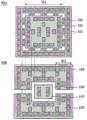
参考图6中的第一金属层1021的俯视互连图案60A,连续金属构件103可由无任何中断或未由除金属之外的材料(例如介电质(层间介电质(ILD)或金属间介电质(IMD)))切断的特定金属区域限定。所述特定金属区域中的距离的测量是连续金属构件103的尺寸。如图1及6中所绘示,从互连图案60A的中心开始朝向图案的外围,连续金属构件103由第一介电构件104切断,且连续金属构件103的尺寸可为由第一介电构件104围封的宽度W1。返回参考图1,就技术节点N14来说,在一些实施例中,连续金属构件103的尺寸W1小于2μm。连续金属构件的尺寸设定为金属图案设计的设计规则。遵循此规则的金属层将从包含金属层中的应力的适当释放的各种设计考虑获益。如图6中的第一金属层1021的俯视互连图案60A中所展示,第一介电构件104显现为具有间断带结构。若干金属桥1031连接第一介电构件104内的连续金属构件103及第一介电构件104外的连续金属构件103。尽管俯视图案60A中未展示,但第一介电构件104外的连续金属构件也遵循上文所论述的小于2μm设计规则。Referring to the top
参考图1,贯穿衬底导通孔(TSV)105从衬底100的无源侧100B朝向有源侧100A延伸且进而与第一金属层1021接触。TSV通常形成于半导体IC裸片中以促进形成三维(3D)堆叠裸片结构。TSV可用于提供3D堆叠裸片结构的不同裸片中的组件之间的电互连。如先前所论述,在技术节点N14中,TSV 105的宽度W3不与互连层102同步缩小,因此,宽度W3大于连续金属构件103的尺寸W1。例如,宽度W3可等于或大于2.4μm,而尺寸W1应小于2μm。TSV 105与第一金属层1021之间的重叠区域是虎齿形成的热点。尽管穿透第一介电构件104的第一组虎齿107可不出现于最终产品中,但其在图1中以虚线绘示。在一些实施例中,穿透连续金属构件103内的第一金属层1021的第二组虎齿109在图1中也以虚线绘示。一般技术人员应了解,所绘示的虎齿107、109仅供展示且不旨在限制半导体结构10的最终互连层。Referring to FIG. 1 , a through-substrate via (TSV) 105 extends from the
参考图2,图2是展示根据本揭露的一些实施例的半导体结构20的互连的剖面图。在图2中,互连层102进一步包含第二金属层1031及第二导通孔层1032,所述两个层安置于半导体衬底100的有源侧100A处且比第一金属层1021更远离有源侧100A。Referring to FIG. 2 , FIG. 2 is a cross-sectional view illustrating interconnections of a
参考图6中的第二金属层1031的俯视互连图案60B,连续金属构件103'可由无任何中断或未由除金属之外的材料(例如介电质(层间介电质(ILD)或金属间介电质(IMD)))切断的特定金属区域限定。所述特定金属区域中的距离的测量是连续金属构件130'的尺寸。如图2及6中所绘示,从第二介电构件104'的内部部分开始朝向图案的外围,连续金属构件103'由第二介电构件104'的外部部分切断,且连续金属构件103'的尺寸可为第二介电构件104'的内部部分与外部部分之间所测量的宽度W2。返回参考图2,就技术节点N14来说,在一些实施例中,连续金属构件103'的尺寸W2小于2μm。连续金属构件的尺寸设定为金属图案设计的设计规则。遵循此规则的金属层将从包含金属层中的应力的适当释放的各种设计考虑获益。如图6中的第二金属层1031的俯视互连图案60B中所展示,第二介电构件104'显现为具有间断带结构。若干金属桥1031'连接第二介电构件104'的内部部分内的连续金属构件103'及第二介电构件104'的内部部分外的连续金属构件103',如这些等。尽管俯视图案60B中未展示,但第二介电构件104'的内部部分内的连续金属构件也遵循上文所论述的小于2μm设计规则。Referring to the top
如图2中所展示,第二介电构件104'及第一介电构件104安置成彼此错开。即,第一金属层1021处的第一介电构件104的竖直投影不与第二金属层1031处的第二介电构件104'重叠。第一介电构件104及第二介电构件104'的此错开布置有效地防止第一组虎齿107穿透到更远离有源侧100A的金属层。As shown in FIG. 2, the second dielectric member 104' and the
参考图3,图3是展示根据本揭露的一些实施例的半导体结构30的互连的剖面图。在图3中,互连层102进一步包含第三金属层1041及第三导通孔层1042,所述两个层安置于半导体衬底100的有源侧100A处且比第二金属层1031更远离有源侧100A。Referring to FIG. 3 , FIG. 3 is a cross-sectional view illustrating interconnections of a
如图3中所展示,第三金属层1041可为无任何中断或未由介电构件切断的连续金属构件。在大于N20的技术节点中,通常采用无介电图案的固体金属层作为第一金属层。在技术节点N14及其以上中,如本文所论述,第三金属层1041开始采用固体金属层。另外,第三金属层1041的厚度可大于第一金属层1021的厚度。例如,第三金属层1041的厚度可为第一金属层1021的厚度的两倍。在一些实施例中,第三金属层1041不必遵循上文所论述的小于2μm设计规则。As shown in FIG. 3 , the
参考图4,图4是展示根据本揭露的一些实施例的半导体结构40的互连的剖面图。在图4中,互连层102进一步包含第三金属层1041及第三导通孔层1042,所述两个层安置于半导体衬底100的有源侧100A处且比第二金属层1031更远离有源侧100A。Referring to FIG. 4 , FIG. 4 is a cross-sectional view illustrating interconnections of a
如图4中所展示,第三金属层1041可具有相同于第一金属层1021的连续金属构件103及第一介电构件104的连续金属构件103”及第三介电构件104”两者。另外,第三金属层1041的厚度可相同于第一金属层1021的厚度。在一些实施例中,第三金属层1041也遵循上文所论述的小于2μm设计规则。即使第三金属层1041及第一金属层1021共享大体上相同的连续金属构件及介电构件,但所述装置安置成相对于第一金属层与第三金属层之间的第二金属层1031错开。本揭露规定:相邻金属层将必须应用错开图案,而非相邻金属层不必受限于此规则。As shown in FIG. 4 , the
参考图5,图5是展示根据本揭露的一些实施例的半导体结构50的互连的剖面图。在图5中,互连层102进一步包含第四金属层1051及第四导通孔层1052,所述两个层安置于半导体衬底100的有源侧100A处且比第三金属层1041更远离有源侧100A。Referring to FIG. 5 , FIG. 5 is a cross-sectional view illustrating interconnections of a
如图5中所展示,第三金属层1041的连续金属构件103”及第三介电构件104”不同于第二金属层1031的连续金属构件103'及第二介电构件104'。另外,第四金属层1051的连续金属构件103”'及第三介电构件104”不同于第三金属层1041的连续金属构件及介电构件。在一些实施例中,第四金属层1051的厚度可相同于第一金属层1021的厚度。在一些实施例中,第四金属层1051也遵循上文所论述的小于2μm设计规则。尽管图5中未绘示,但在一些实施例中,第三金属层1041的连续金属构件103”及第三介电构件104”可大体上相同于第一金属层1021的连续金属构件及介电构件且第四金属层1051的连续金属构件103”'及第四介电构件104”'可大体上相同于第二金属层1031的连续金属构件及介电构件。在本发明实施例中,更远离有源侧100A的一第五金属层(图中未展示)可具有固体金属图案及大于2μm的设计规则,如先前所论述。As shown in FIG. 5 , the
在技术节点N14及其以上的前提下遵循上文所论述的小于2μm设计规则。然而,在技术节点N7中,金属层的设计规则可(例如)小于0.5μm。换句话说,就技术节点N7来说,遵循设计规则的金属层中的连续金属构件的尺寸应小于0.5μm。The sub-2 μm design rules discussed above are followed on the premise of technology node N14 and above. However, in technology node N7, the design rule for the metal layer may be, for example, smaller than 0.5 μm. In other words, as far as technology node N7 is concerned, the size of the continuous metal member in the metal layer following the design rules should be smaller than 0.5 μm.
参考图6,图6是展示根据本揭露的一些实施例的两个相邻层的两个互连图案结构60A、60B的俯视图。如先前所论述,互连图案结构60A是图1及2中所展示的第一金属层1021的俯视图,而互连图案结构60B是图2中所展示的第二金属层1031的俯视图。相同于先前所提及的元件符号的元件符号表示大体上相同组件,且为简洁起见,此处不再重复。使用对准虚线绘示图案结构60A及60B以展示将第一介电构件104向下投影到第二金属层1031的连续金属构件103'。另一方面,将第二介电构件104'的内部部分及外部部分向上投影到第一金属层1021的连续金属构件103。可在图6中清楚地看到第一介电构件104及第二介电构件104'的错开安置。此外,还从图6的俯视视角展示第一导通孔层1022及第二导通孔层1032。如先前所论述,第一介电构件104及第二介电构件104'具有间断带。Referring to FIG. 6 , FIG. 6 is a top view showing two
参考图7,图7是展示根据本揭露的一些实施例的两个相邻层的两个互连图案结构70A、70B的俯视图。如先前所论述,互连图案结构70A是图1及2中所展示的第一金属层1021的俯视图,而互连图案结构70B是图2中所展示的第二金属层1031的俯视图。在一些实施例中,第一介电构件104及第二介电构件104'显现为具有闭合带结构。无金属桥连接第一介电构件104内的连续金属构件103及第一介电构件104外的连续金属构件103。类似地,无金属桥连接第二介电构件104'的内部部分内的连续金属构件103'及第二介电构件104'的内部部分外的连续金属构件103'。使用对准虚线绘示图案结构70A及70B以展示将第一介电构件104向下投影到第二金属层1031的连续金属构件103'。另一方面,将第二介电构件104'的内部部分及外部部分向上投影到第一金属层1021的连续金属构件103。尽管俯视图案60B中未展示,但第二介电构件104'的内部部分内的连续金属构件还遵循上文所论述的小于2μm设计规则。Referring to FIG. 7 , FIG. 7 is a top view showing two
参考图8,图8是展示根据本揭露的一些实施例的两个相邻层的互连图案结构80A、80B的俯视图。如先前所论述,互连图案结构80A是图1及2中所展示的第一金属层1021的俯视图,而互连图案结构80B是图2中所展示的第二金属层1031的俯视图。在一些实施例中,第一介电构件104显现为具有断开带结构。若干介电桥将第一介电构件104连接到第一介电构件104的另一部分(图中未展示)。然而,为维持相邻金属层之间的错开特征,第二介电构件104'显现为具有闭合带结构。使用对准虚线绘示图案结构80A、80B以展示将第一介电构件104向下投影到第二金属层1031的连续金属构件103'。另一方面,将第二介电构件104'的内部部分及外部部分向上投影到第一金属层1021的连续金属构件103。Referring to FIG. 8 , FIG. 8 is a top view showing
参考图9,图9是展示根据本揭露的一些实施例的两个相邻层的互连图案结构90A、90B的俯视图。如先前所论述,互连图案结构90A是图1及2中所展示的第一金属层1021的俯视图,而互连图案结构90B是图2中所展示的第二金属层1031的俯视图。在一些实施例中,第一介电构件104显现为具有间断带结构。若干金属桥1031连接第一介电构件104内的连续金属构件103及第一介电构件104外的连续金属构件103。为维持相邻金属层之间的错开特征,第二介电构件104'显现为具有断开带结构。使用对准虚线绘示图案结构90A、90B以展示将第一介电构件104向下投影到第二金属层1031的连续金属构件103'。另一方面,将第二介电构件104'的内部部分及外部部分向上投影到第一金属层1021的连续金属构件103。Referring to FIG. 9 , FIG. 9 is a top view showing
图10到14是根据本揭露的一些实施例的各种制造操作中的半导体结构30的剖面图。在图10中,接收具有有源侧100A及无源侧100B的半导体衬底100。如先前所论述,将例如存储器或晶体管的有源组件定位于有源侧100A接近处,使用于使不同有源区域分离的绝缘层101(例如浅沟槽隔离区)还形成于衬底的有源侧100A接近处。随后,可使例如层间介电质(ILD)的介电层101形成于绝缘层101及衬底100上方。在介电层101上方,制造具有各金属层的先前所论述图案的装置的互连层102。在图10所绘示的实施例中,形成三个金属层及导通孔层。在一些实施例中,金属层是例如金属线、金属导通孔构件或金属接点构件的金属构件。10-14 are cross-sectional views of
例如,通过镶嵌过程来形成第一金属层1021,如下文将进一步描述。使第一介电材料层形成于介电层101上。替代地,使蚀刻停止层(图中未展示)形成于介电层101上且使第一介电材料层形成于蚀刻停止层上。在一些实施例中,第一介电材料层包含例如氧化硅、氮化硅、低介电系数(低k)材料或其组合的介电材料。低k材料可包含(例如)掺氟硅玻璃(FSG)、掺碳氧化硅、Black 
其后,通过光刻过程来图案化第一金属层1021的掩模层(图中未展示),借此形成具有一(或多个)开口的一图案化掩模层以限定一(或若干)金属线的一(或若干)区域,如图6到9中所绘示。在一些实施例中,图案化掩模层的开口对应于第一金属层1021中的连续金属构件103的位置,且图案化掩模层的覆盖区域对应于第一金属层1021中的第一介电构件104的位置。金属线是指待形成的上金属层中的金属线。在一些实施例中,掩模层为光阻层,图案化过程是包含旋涂涂覆、曝光及显影的光刻过程。在一些实施例中,掩模层为硬掩模,图案化过程包含:使用光刻过程使图案化光阻层形成于硬掩模上;及使用图案化光阻层作为蚀刻掩模,透过图案化光阻层的开口蚀刻硬掩模。在形成图案化硬掩模之后,可通过等离子体灰化或湿式剥离来移除图案化光阻层。Thereafter, the mask layer (not shown) of the
第一导通孔层1022的形成可参考先前关于第一金属层1021的形成所论述的段落,且为简洁起见,此处不再重复。当然,第一导通孔层1022的图案化随第一金属层1021的图案化而对应改变。第二金属层1031的形成可参考先前关于第一金属层1021的形成所论述的段落,且为简洁起见,此处不再重复。第二金属层1031的图案包含连续金属构件103'及第二介电构件104',如先前所描述。第一金属层1021中的第一介电构件104经设计以与第二金属层1031中的第二介电构件104'错开安置。此外,在图10中,第三金属层1041的形成可参考先前关于第一金属层1021的形成所论述的段落,且为简洁起见,此处不再重复。在一些实施例中,第三金属层1041可为无任何中断或未由介电构件切断的连续金属构件。For the formation of the first via
在一些实施例中,可接着透过例如背面研磨、蚀刻、CMP或其类似者的已知技术从无源侧100B薄化衬底100,且使厚钝化层100'(例如氧化物层)形成于无源侧100B上的薄化表面上方。In some embodiments, the
在图11中,经由第一蚀刻操作从衬底100的无源侧100B部分形成贯穿衬底导通孔(TSV)凹槽105'。第一蚀刻操作从无源侧100B移除衬底100,直到到达绝缘层303。在一些实施例中,第一蚀刻操作利用适合于移除衬底材料的蚀刻化学作用。在衬底100的有源侧100A接近处形成CMOS装置之后及在互连层102中形成金属层(例如至少M1到M3)的金属化过程之后形成TSV凹槽105'。在使用先进处理技术所制造的IC中,金属间介电(IMD)层1013通常由具有低介电系数(低k)或极低介电系数的介电材料形成以试图减少金属层间寄生电容以因此提高信号速度及增强信号完整性。作为一实例,低k介电材料具有小于2.9的介电系数且由多孔有机介电材料形成。In FIG. 11 , a through substrate via (TSV)
在图12中,经由第二蚀刻操作从衬底100的无源侧100B完全形成贯穿衬底导通孔(TSV)凹槽105”。第二蚀刻操作移除剩余绝缘层303、介电层303,直到到达第一金属层1021。在一些实施例中,第二蚀刻操作利用不同于第一蚀刻操作的蚀刻化学作用的蚀刻化学作用,例如,第二蚀刻操作利用适合于移除介电材料的化学作用。其能够控制确定虎齿形成的第二蚀刻。例如,如果第二蚀刻被视为过蚀刻,那么第一金属层1021层级及第一导通孔层1022处的IMD层1013可由蚀刻剂移除以提供由后续金属材料填充的虎齿凹穴。第一金属层1021层级处的IMD层1013对应于先前所论述的第一介电构件104。In FIG. 12, a through-substrate via (TSV)
此TSV凹槽105”形成过程在先进处理技术中产生若干问题。问题之一是在金属间介电层中形成TSV凹槽105”通常涉及多个蚀刻过程;处理中的晶片通常要排队等待各种蚀刻过程完成。在处理期间,晶片处理设施中的水分或其它化学试剂可从TSV凹槽的侧壁渗出到低k金属间介电层中且在金属间介电层中扩散,其会导致低k介电材料的非所要特性变化。归因于TSV凹槽的大暴露表面积,此有害效应会较为显著且引起严重装置性能降级及良率损失。此处所提供的第一蚀刻及第二蚀刻提供通过在TSV凹槽105”形成的最后蚀刻操作中暴露低k IMD层1013来减少IMD层1013的特性变化的方法。This
随后,通过例如金属化学气相沉积过程(CVD)或金属电镀过程的金属化过程来使形成于IMD层及衬底100中的TSV凹槽105”填充导电金属材料。随后,可对衬底100的无源侧100B执行例如金属CVD或金属镀覆的金属化过程以在TSV凹槽105”中填充铜(Cu)或适合导电材料以在衬底100中形成TSV 105。还可使用其它适合导电材料(例如铝(Al)、钨(W)、钴(Co)、金(Au)、银(Ag)、铂(Pt)、硅(Si))及其它适合沉积过程形成TSV 105。Subsequently, the
接着,在图13中,可对衬底100的无源侧100B执行CMP操作以移除过量TSV材料且提供用于后续处理操作的所要平坦衬底表面。在形成TSV 105的金属化过程之前,可通过例如CVD或物理气相沉积(PVD)的适合过程来使例如氮化钛(TiN)层及/或金属晶种层(图中未展示)的阻障层任选地保形地形成于TSV凹槽105”中。TSV凹槽105”中的阻障层可防止任何导电TSV材料渗出到衬底100的有源侧100A处的电路的任何有源部分中。还如图13中所展示,使用虚线绘示第一组虎齿107以展示可能位置及第二金属层1031可如何有效防止第一组虎齿107朝向较高金属层进一步穿透。Next, in Figure 13, a CMP operation may be performed on the
在图14中,可进一步处理衬底100的无源侧100B以形成绝缘层116、介电层(图中未展示)、导电界面(图中未展示)、接垫(图中未展示),其中类似材料及处理技术用于先前形成于衬底100的有源侧100A上方的类似装置。因此所处理的衬底100可从两侧接合到其它集成电路晶片及裸片。还如图14中所展示,在金属化过程之后,接近第一金属层1021的TSV105的宽度W3大于第一金属层1021的第一介电构件104的尺寸。由于“虎齿”导通孔穿通不再成问题,所以可放宽用于形成TSV 105的处理窗且还可提高装置性能。In FIG. 14, the
一些实施例提供一种半导体结构,其包含:半导体衬底,其具有有源侧;互连层,其位于所述半导体衬底的所述有源侧上方;及贯穿衬底导通孔(TSV),其从所述半导体衬底延伸到第一金属层。所述互连层包含最靠近所述半导体衬底的所述有源侧的第一金属层,所述第一金属层的厚度低于1微米,且从俯视视角看,所述第一金属层的连续金属构件的尺寸小于2微米。所述连续金属构件由第一介电构件切断。Some embodiments provide a semiconductor structure comprising: a semiconductor substrate having an active side; an interconnect layer over the active side of the semiconductor substrate; and a through-substrate via (TSV) ) extending from the semiconductor substrate to the first metal layer. The interconnection layer includes a first metal layer closest to the active side of the semiconductor substrate, the thickness of the first metal layer is less than 1 micron, and from a top view, the first metal layer The size of the continuous metal member is less than 2 microns. The continuous metal member is severed by the first dielectric member.
一些实施例提供一种互连图案结构,其包含第一金属层及所述第一金属层上方的第二金属层。从俯视视角看,所述第一金属层的连续金属构件的尺寸小于2微米。所述连续金属构件由第一介电构件切断。从俯视视角看,所述第二金属层的连续金属构件的尺寸小于2微米。所述连续金属构件由第二介电构件切断。所述第二介电构件安置成与所述第一介电构件错开。Some embodiments provide an interconnect pattern structure including a first metal layer and a second metal layer above the first metal layer. The size of the continuous metal members of the first metal layer is less than 2 microns when viewed from a top view. The continuous metal member is severed by the first dielectric member. Viewed from a top view, the size of the continuous metal member of the second metal layer is less than 2 microns. The continuous metal member is severed by the second dielectric member. The second dielectric member is disposed to be offset from the first dielectric member.
一些实施例提供一种用于制造半导体结构的方法。所述方法包含:接收具有有源侧的半导体衬底;形成最靠近所述半导体衬底的所述有源侧的第一金属层,其中第一介电构件切断所述第一金属层的连续金属构件;形成位于所述半导体衬底的所述有源侧处且比所述第一金属层更远离所述有源侧的第二金属层,其中第二介电构件切断所述第二金属层的连续金属构件。所述第二介电构件安置成与所述第一介电构件错开。形成从所述半导体衬底延伸到所述第一金属层的贯穿衬底导通孔(TSV)。Some embodiments provide a method for fabricating a semiconductor structure. The method includes: receiving a semiconductor substrate having an active side; forming a first metal layer proximate to the active side of the semiconductor substrate, wherein a first dielectric member cuts off the continuity of the first metal layer a metal member; forming a second metal layer located at the active side of the semiconductor substrate and farther from the active side than the first metal layer, wherein a second dielectric member cuts off the second metal Layers of continuous metal components. The second dielectric member is disposed to be offset from the first dielectric member. A through-substrate via (TSV) is formed extending from the semiconductor substrate to the first metal layer.
尽管已详细描述本发明实施例及其优点,但应了解,可在不背离由随附权利要求书限定的本发明实施例的精神及范围的情况下对本文进行各种改变、替代及更改。例如,上文所论述的诸多过程可以不同方法实施且由其它过程或其组合替换。Although embodiments of the present invention and their advantages have been described in detail, it should be understood that various changes, substitutions and alterations can be made herein without departing from the spirit and scope of the embodiments of the invention as defined by the appended claims. For example, many of the processes discussed above can be implemented in different ways and replaced by other processes or combinations thereof.
再者,本申请案的范围不旨在受限于本说明书中所描述的过程、机器、制造、物质组成、措施、方法及步骤的特定实施例。一般技术人员应易于从本发明实施例的揭露了解,可根据本发明实施例利用现存或后来发展的过程、机器、制造、物质组成、措施、方法或步骤,其执行大体上相同于本文所描述的对应实施例的功能或达成大体上相同于本文所描述的对应实施例的结果。因此,随附权利要求书旨在将这些过程、机器、制造、物质组成、措施、方法或步骤包含于其范围内。Furthermore, the scope of the present application is not intended to be limited to the particular embodiments of the process, machine, manufacture, composition of matter, means, methods and steps described in the specification. Those of ordinary skill should easily understand from the disclosure of the embodiments of the present invention that existing or later developed processes, machines, manufactures, compositions of matter, measures, methods or steps can be used according to the embodiments of the present invention, and its execution is substantially the same as that described herein The function of the corresponding embodiment of or achieve substantially the same result as the corresponding embodiment described herein. Accordingly, the appended claims are intended to include within their scope such processes, machines, manufacture, compositions of matter, means, methods, or steps.
附图标记reference sign
10 半导体结构10 Semiconductor structure
20 半导体结构20 Semiconductor structure
30 半导体结构30 Semiconductor structure
40 半导体结构40 Semiconductor Structure
50 半导体结构50 semiconductor structure
60A 互连图案结构60A Interconnect pattern structure
60B 互连图案结构60B Interconnect Pattern Structure
70A 互连图案结构70A Interconnect pattern structure
70B 互连图案结构70B Interconnect pattern structure
80A 互连图案结构80A Interconnect pattern structure
80B 互连图案结构80B Interconnect pattern structure
90A 互连图案结构90A Interconnect pattern structure
90B 互连图案结构90B Interconnect pattern structure
100 衬底100 substrate
100' 钝化层100' passivation layer
100A 有源侧100A active side
100B 无源侧100B passive side
101 绝缘层/介电层101 insulating layer / dielectric layer
102 互连层102 Interconnect layer
103 连续金属构件103 Continuous metal components
103' 连续金属构件103' continuous metal member
103” 连续金属构件103” continuous metal member
103”' 连续金属构件103”' continuous metal member
104 第一介电构件104 first dielectric member
104' 第二介电构件104' Second Dielectric Member
104” 第三介电构件104” third dielectric member
104”' 第四介电构件104"' fourth dielectric member
105 贯穿衬底导通孔(TSV)105 Through Substrate Via (TSV)
105' TSV凹槽105' TSV groove
105” TSV凹槽105” TSV groove
107 第一组虎齿107 The first set of tiger teeth
109 第二组虎齿109 The second set of tiger teeth
116 绝缘层116 insulation layer
303 绝缘层/介电层303 insulating layer / dielectric layer
1013 介电质/金属间介电(IMD)层1013 Dielectric/Intermetal Dielectric (IMD) layer
1021 第一金属层1021 first metal layer
1022 第一导通孔层1022 The first via layer
1031 金属桥/第二金属层1031 metal bridge/second metal layer
1031' 金属桥1031' metal bridge
1032 第二导通孔层1032 Second via layer
1041 第三金属层1041 The third metal layer
1042 第三导通孔层1042 The third via layer
1051 第四金属层1051 fourth metal layer
1052 第四导通孔层1052 The fourth via layer
T1 厚度T1 Thickness
W1 宽度/尺寸W1 Width/Size
W2 宽度/尺寸W2 Width/Size
W3 宽度W3 width
Claims (20)
Applications Claiming Priority (4)
| Application Number | Priority Date | Filing Date | Title |
|---|---|---|---|
| US201762579030P | 2017-10-30 | 2017-10-30 | |
| US62/579,030 | 2017-10-30 | ||
| US15/841,945 | 2017-12-14 | ||
| US15/841,945 US10163758B1 (en) | 2017-10-30 | 2017-12-14 | Semiconductor structure and manufacturing method for the same |
Publications (2)
| Publication Number | Publication Date |
|---|---|
| CN109727952A CN109727952A (en) | 2019-05-07 |
| CN109727952B true CN109727952B (en) | 2023-04-14 |
Family
ID=64692220
Family Applications (1)
| Application Number | Title | Priority Date | Filing Date |
|---|---|---|---|
| CN201810926996.7A Active CN109727952B (en) | 2017-10-30 | 2018-08-15 | Interconnection pattern structure, semiconductor structure and manufacturing method thereof |
Country Status (5)
| Country | Link |
|---|---|
| US (3) | US10163758B1 (en) |
| KR (1) | KR102319994B1 (en) |
| CN (1) | CN109727952B (en) |
| DE (1) | DE102018124699B4 (en) |
| TW (1) | TWI665744B (en) |
Families Citing this family (1)
| Publication number | Priority date | Publication date | Assignee | Title |
|---|---|---|---|---|
| US11942368B2 (en) * | 2021-02-26 | 2024-03-26 | Taiwan Semiconductor Manufacturing Company, Ltd. | Through silicon vias and methods of fabricating thereof |
Citations (4)
| Publication number | Priority date | Publication date | Assignee | Title |
|---|---|---|---|---|
| CN104218021A (en) * | 2013-06-04 | 2014-12-17 | 格罗方德半导体公司 | Circuit structures and methods of fabrication with enhanced contact via electrical connection |
| CN104838495A (en) * | 2012-12-21 | 2015-08-12 | 英特尔公司 | Landing structure for through-silicon via |
| JP2016035948A (en) * | 2014-08-01 | 2016-03-17 | マイクロン テクノロジー, インク. | Semiconductor device and method of manufacturing the same |
| CN108701614A (en) * | 2016-02-29 | 2018-10-23 | Towerjazz松下半导体有限公司 | Semiconductor device and manufacturing method thereof |
Family Cites Families (20)
| Publication number | Priority date | Publication date | Assignee | Title |
|---|---|---|---|---|
| TW442873B (en) * | 1999-01-14 | 2001-06-23 | United Microelectronics Corp | Three-dimension stack-type chip structure and its manufacturing method |
| JP4965443B2 (en) * | 2005-06-30 | 2012-07-04 | スパンション エルエルシー | Manufacturing method of semiconductor device |
| US7968975B2 (en) * | 2008-08-08 | 2011-06-28 | International Business Machines Corporation | Metal wiring structure for integration with through substrate vias |
| JP5147779B2 (en) * | 2009-04-16 | 2013-02-20 | 新光電気工業株式会社 | Wiring board manufacturing method and semiconductor package manufacturing method |
| US8378450B2 (en) * | 2009-08-27 | 2013-02-19 | International Business Machines Corporation | Interdigitated vertical parallel capacitor |
| US8513767B2 (en) * | 2011-03-21 | 2013-08-20 | Globalfoundries Singapore Pte. Ltd. | Package interconnects |
| US9177914B2 (en) * | 2012-11-15 | 2015-11-03 | Taiwan Semiconductor Manufacturing Company, Ltd. | Metal pad structure over TSV to reduce shorting of upper metal layer |
| US20150021773A1 (en) * | 2013-07-22 | 2015-01-22 | Conversant Intellectual Property Management Inc. | Through Semiconductor via Structure with Reduced Stress Proximity Effect |
| JP6292049B2 (en) | 2013-09-02 | 2018-03-14 | ソニー株式会社 | Semiconductor device and manufacturing method thereof |
| US9754918B2 (en) * | 2014-05-09 | 2017-09-05 | Taiwan Semiconductor Manufacturing Company, Ltd. | 3D chip-on-wafer-on-substrate structure with via last process |
| US9666520B2 (en) * | 2014-04-30 | 2017-05-30 | Taiwan Semiconductor Manufactuing Company, Ltd. | 3D stacked-chip package |
| US9543257B2 (en) | 2014-05-29 | 2017-01-10 | Taiwan Semiconductor Manufacturing Company, Ltd. | 3DIC interconnect devices and methods of forming same |
| US20150348874A1 (en) * | 2014-05-29 | 2015-12-03 | Taiwan Semiconductor Manufacturing Company, Ltd. | 3DIC Interconnect Devices and Methods of Forming Same |
| JP6468071B2 (en) * | 2015-05-25 | 2019-02-13 | 富士通株式会社 | Semiconductor device, electronic device, and method of manufacturing semiconductor device |
| JP6489942B2 (en) | 2015-05-29 | 2019-03-27 | 東芝メモリ株式会社 | Manufacturing method of semiconductor device |
| US9536810B1 (en) | 2015-06-12 | 2017-01-03 | Taiwan Semiconductor Manufacturing Co., Ltd. | Flat pad structure for integrating complementary metal-oxide-semiconductor (CMOS) image sensor processes |
| KR102387948B1 (en) | 2015-08-06 | 2022-04-18 | 삼성전자주식회사 | Integrated circuit device having through-silicon via structure |
| US10170461B2 (en) * | 2015-11-16 | 2019-01-01 | Taiwan Semiconductor Manufacturing Co., Ltd. | ESD hard backend structures in nanometer dimension |
| US10147682B2 (en) * | 2015-11-30 | 2018-12-04 | Taiwan Semiconductor Manufacturing Co., Ltd. | Structure for stacked logic performance improvement |
| US20170170215A1 (en) * | 2015-12-15 | 2017-06-15 | Taiwan Semiconductor Manufacturing Co., Ltd. | Semiconductor device structure with anti-acid layer and method for forming the same |
-
2017
- 2017-12-14 US US15/841,945 patent/US10163758B1/en active Active
-
2018
- 2018-07-03 TW TW107122984A patent/TWI665744B/en active
- 2018-08-15 CN CN201810926996.7A patent/CN109727952B/en active Active
- 2018-10-08 DE DE102018124699.4A patent/DE102018124699B4/en active Active
- 2018-10-30 KR KR1020180130913A patent/KR102319994B1/en active Active
- 2018-12-20 US US16/228,585 patent/US10727164B2/en active Active
-
2020
- 2020-07-03 US US16/920,430 patent/US11387167B2/en active Active
Patent Citations (4)
| Publication number | Priority date | Publication date | Assignee | Title |
|---|---|---|---|---|
| CN104838495A (en) * | 2012-12-21 | 2015-08-12 | 英特尔公司 | Landing structure for through-silicon via |
| CN104218021A (en) * | 2013-06-04 | 2014-12-17 | 格罗方德半导体公司 | Circuit structures and methods of fabrication with enhanced contact via electrical connection |
| JP2016035948A (en) * | 2014-08-01 | 2016-03-17 | マイクロン テクノロジー, インク. | Semiconductor device and method of manufacturing the same |
| CN108701614A (en) * | 2016-02-29 | 2018-10-23 | Towerjazz松下半导体有限公司 | Semiconductor device and manufacturing method thereof |
Also Published As
| Publication number | Publication date |
|---|---|
| DE102018124699A1 (en) | 2019-05-02 |
| KR20190049559A (en) | 2019-05-09 |
| DE102018124699B4 (en) | 2023-07-27 |
| KR102319994B1 (en) | 2021-11-03 |
| US11387167B2 (en) | 2022-07-12 |
| CN109727952A (en) | 2019-05-07 |
| TWI665744B (en) | 2019-07-11 |
| US10163758B1 (en) | 2018-12-25 |
| US20200335427A1 (en) | 2020-10-22 |
| US20190148266A1 (en) | 2019-05-16 |
| TW201917801A (en) | 2019-05-01 |
| US10727164B2 (en) | 2020-07-28 |
Similar Documents
| Publication | Publication Date | Title |
|---|---|---|
| US10861742B2 (en) | Interconnect structure having an etch stop layer over conductive lines | |
| US10504776B2 (en) | Methods for forming through-substrate vias penetrating inter-layer dielectric | |
| TWI727383B (en) | Semiconductor structure, 3dic structure and method of fabricating the same | |
| US9847256B2 (en) | Methods for forming a device having a capped through-substrate via structure | |
| CN107452672B (en) | Semiconductor structure, method of manufacturing the same, and method of manufacturing seal ring structure | |
| US20170186704A1 (en) | Method for manufacturing a semiconductor device having moisture-resistant rings being formed in a peripheral region | |
| TWI681506B (en) | Field effect transistor device and manufacturing method thereof | |
| US20130270712A1 (en) | Through silicon via structure and method of fabricating the same | |
| CN103515302B (en) | Semiconductor device and method of manufacture | |
| TWI873767B (en) | Semiconductor device having inductor and method of manufacturing thereof | |
| US20250349618A1 (en) | Redistribution layer metallic structure and method | |
| CN109727952B (en) | Interconnection pattern structure, semiconductor structure and manufacturing method thereof | |
| CN112435977B (en) | Semiconductor device and manufacturing method thereof |
Legal Events
| Date | Code | Title | Description |
|---|---|---|---|
| PB01 | Publication | ||
| PB01 | Publication | ||
| SE01 | Entry into force of request for substantive examination | ||
| SE01 | Entry into force of request for substantive examination | ||
| GR01 | Patent grant | ||
| GR01 | Patent grant | ||
| TG01 | Patent term adjustment |
Free format text: NEW EXPIRY DATE: 20390414 |
|
| TG01 | Patent term adjustment |