Disclosure of Invention
The following presents a simplified summary of one or more aspects in order to provide a basic understanding of such aspects. This summary is not an extensive overview of all contemplated aspects, and is intended to neither identify key or critical elements of all aspects nor delineate the scope of any or all aspects. Its sole purpose is to present some concepts of one or more aspects in a simplified form as a prelude to the more detailed description that is presented later.
In order to overcome the above-mentioned defects of the prior art, the present invention provides a three-dimensional memory and a method for manufacturing the three-dimensional memory.
The manufacturing method of the three-dimensional memory provided by the invention comprises the following steps:
providing a first wafer and a second wafer, wherein the first wafer comprises a first substrate and a first dielectric layer, and the upper part of the second wafer is a peripheral device of the three-dimensional memory;
forming a well region of an array unit of the three-dimensional memory in the first dielectric layer, and forming the array unit on the upper part of the first wafer;
bonding the first wafer and the second wafer, wherein a first bonding interface is formed between the array unit and the peripheral device;
and cutting the first wafer along a first cutting interface between the first dielectric layer and the first substrate, so that the first wafer is peeled off from the first substrate.
Preferably, in the method for manufacturing the three-dimensional memory provided by the present invention, the step of providing the first wafer may further include:
providing the first substrate and the third substrate;
forming the first dielectric layer in the third substrate;
bonding the first substrate and the third substrate, wherein a second bonding interface is formed between the first substrate and the first dielectric layer;
and cutting the third substrate by taking the interface of the first dielectric layer in the third substrate as a second cutting interface, so that the first dielectric layer is stripped from the third substrate.
Preferably, in the method for manufacturing a three-dimensional memory according to the present invention, the forming the first dielectric layer in the third substrate may further include:
and carrying out hydrogen injection treatment on the surface of the third substrate to form a hydrogen injection layer, wherein the first dielectric layer is the hydrogen injection layer.
Preferably, in the method for manufacturing the three-dimensional memory provided by the present invention, the step of forming the well region of the array unit of the memory in the first dielectric layer may further include:
performing ion implantation on the hydrogen implantation layer to form the well region;
and high-temperature annealing to solidify the PN junction in the well region and degas the hydrogen injection layer to form a hydrogen-rich layer.
Optionally, in the method for manufacturing the three-dimensional memory provided by the present invention, providing the first substrate may further include:
porous oxidation treatment is performed in the first substrate to form a porous silicon oxide layer.
Alternatively, in the method for manufacturing a three-dimensional memory according to the present invention, the bonding the first substrate and the third substrate may further include:
and inverting the third substrate to adhere the first dielectric layer to the upper surface of the first substrate.
Optionally, in the method for manufacturing a three-dimensional memory provided by the present invention, after the cutting the third substrate, the method may further include:
and polishing the second cutting interface.
Optionally, in the method for manufacturing a three-dimensional memory provided by the present invention, after the cutting the first wafer, the method may further include:
and polishing the surface of the first dielectric layer.
Alternatively, in the method for manufacturing the three-dimensional memory provided by the present invention, the polishing process may be chemical mechanical polishing.
Optionally, in the method for manufacturing a three-dimensional memory provided by the present invention, bonding the first wafer and the second wafer may further include:
and inverting the first wafer to enable the array unit to be bonded on the upper surface of the peripheral device, wherein the stripped first substrate is positioned on the top.
Optionally, in the method for manufacturing a three-dimensional memory according to the present invention, the bonding the first wafer and the second wafer may further include:
inverting the second wafer to bond the peripheral device to the upper surface of the array unit;
the step of dicing the first wafer may further include:
and inverting the bonded first wafer and the bonded second wafer, wherein the peeled first substrate is positioned on the top.
Alternatively, in the method for manufacturing the three-dimensional memory provided by the present invention, the cutting may be performed by a smart cut (smart cut) method.
According to another aspect of the present invention, there is also provided a three-dimensional memory, which can be manufactured by any one of the above manufacturing methods.
Drawings
Fig. 1A shows a schematic structural diagram of a conventional three-dimensional memory before thinning the back surface of a substrate.
Fig. 1B shows a schematic structural diagram of a conventional three-dimensional memory after thinning the back surface of a substrate.
Fig. 1C shows a schematic structure of a conventional three-dimensional memory after a backside metal pad is led out.
Fig. 2 is a flow chart illustrating a method for manufacturing a three-dimensional memory according to an embodiment of the invention.
Fig. 3 is a schematic flow chart of obtaining a first wafer according to an embodiment of the present invention.
Fig. 4 illustrates a schematic flow chart of forming a well region according to an embodiment of the present invention.
Fig. 5A is a schematic diagram illustrating the formation of a first dielectric layer in a third substrate according to an embodiment of the invention.
Fig. 5B is a schematic structural diagram of a third substrate with a first dielectric layer according to an embodiment of the present invention.
Fig. 5C shows a schematic structural diagram of a first substrate with a porous silicon oxide layer according to an embodiment of the present invention.
Fig. 5D shows a schematic diagram of bonding a first substrate and a third substrate provided by one embodiment of the invention.
Fig. 5E shows a schematic diagram of peeling off the third substrate provided by an embodiment of the present invention.
Fig. 5F shows a schematic structural diagram of a first wafer according to an embodiment of the present invention.
Fig. 5G shows a schematic structural diagram of a first wafer with array units according to an embodiment of the present invention.
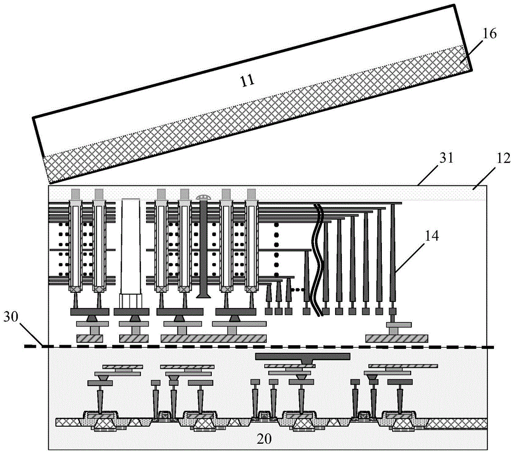
Fig. 5H shows a schematic diagram of bonding a first wafer and a second wafer according to an embodiment of the invention.
Fig. 5I shows a schematic diagram of peeling off the first substrate provided by an embodiment of the present invention.
Fig. 5J illustrates a schematic structural diagram of a three-dimensional memory according to an embodiment of the present invention.
Fig. 6 is a schematic diagram illustrating a well structure of a three-dimensional memory array cell according to an embodiment of the invention.
Reference numerals:
1a silicon substrate;
2 array units;
3 bonding the interface;
4, a CMOS wafer;
5a back metal pad;
10 a first wafer;
11 a first substrate;
12 a first dielectric layer;
131 dielectric silicon oxide;
132 high voltage P-well;
133 high voltage N-well;
134 deep N-well;
135 epitaxial crystalline silicon substrate;
14 array units;
15 a third substrate;
16 a porous silica layer;
20 a second wafer;
21 peripheral devices;
30 a first bonding interface;
31 a first cutting interface;
32 a second bonding interface;
33 a second cutting interface;
201-206 steps of a method for manufacturing a three-dimensional memory;
2011-2016 obtaining a first wafer;
2021-2022 step of forming a well region.
Detailed Description
The following description of the embodiments of the present invention is provided for illustrative purposes, and other advantages and effects of the present invention will become apparent to those skilled in the art from the present disclosure. While the invention will be described in connection with the preferred embodiments, there is no intent to limit its features to those embodiments. On the contrary, the invention is described in connection with the embodiments for the purpose of covering alternatives or modifications that may be extended based on the claims of the present invention. In the following description, numerous specific details are set forth in order to provide a thorough understanding of the present invention. The invention may be practiced without these particulars. Moreover, some of the specific details have been left out of the description in order to avoid obscuring or obscuring the focus of the present invention.
In the description of the present invention, it should be noted that, unless otherwise explicitly specified or limited, the terms "mounted," "connected," and "connected" are to be construed broadly, e.g., as meaning either a fixed connection, a removable connection, or an integral connection; can be mechanically or electrically connected; they may be connected directly or indirectly through intervening media, or they may be interconnected between two elements. The specific meanings of the above terms in the present invention can be understood in specific cases to those skilled in the art.
Additionally, the terms "upper," "lower," "left," "right," "top," "bottom," "horizontal," "vertical" and the like as used in the following description are to be understood as referring to the segment and the associated drawings in the illustrated orientation. The relative terms are used for convenience of description only and do not imply that the described apparatus should be constructed or operated in a particular orientation and therefore should not be construed as limiting the invention.
The terms "over.," under., "" between., "(between)," and ". on.," as used herein refer to the relative position of this layer with respect to other layers. Likewise, for example, a layer deposited or placed over or under another layer may be directly in contact with the other layer or may have one or more intervening layers. Further, a layer deposited or placed between layers may be directly in contact with the layers or may have one or more intervening layers. In contrast, a first layer "on" a second layer is in contact with the second layer. In addition, the relative position of one layer with respect to the other layers is provided (assuming deposition, modification and removal of the thin film operations with respect to the starting substrate without regard to the absolute orientation of the substrate).
It will be understood that, although the terms first, second, third, etc. may be used herein to describe various elements, regions, layers and/or sections, these elements, regions, layers and/or sections should not be limited by these terms, but rather are used to distinguish one element, region, layer and/or section from another element, region, layer and/or section. Thus, a first component, region, layer or section discussed below could be termed a second component, region, layer or section without departing from some embodiments of the present invention.
In order to overcome the above-mentioned drawbacks of the prior art, the present invention provides embodiments of a three-dimensional memory and a method for manufacturing the three-dimensional memory.
As shown in fig. 2, the method for manufacturing a three-dimensional memory according to this embodiment may include:
201: a first wafer 10 and a second wafer 20 are provided.
The first wafer 10 (shown in fig. 5F) includes: a first substrate 11 and a first dielectric layer 12, the first substrate 11 being made of a suitable material including, but not limited to, silicon germanium, germanium or silicon-on-insulator thin film (SOI).
The second wafer 20 (shown in fig. 5H) may include: and a peripheral device 21 disposed on the second wafer 20, wherein the peripheral device 21 includes a plurality of transistors, and the plurality of transistors may be CMOS transistors. It will be appreciated by those skilled in the art that the second wafer 20 may further include a peripheral interconnect layer leading out of the peripheral devices 21, and that the peripheral devices 21 and/or the peripheral interconnect layer may be formed by existing or future-technology semiconductor manufacturing processes.
The peripheral interconnection layer covers the transistors for electrical signal conduction, and includes one or more interlayer insulating layers. The peripheral interconnect layer may further include one or more contacts in an interlayer insulating layer, and one or more interconnect conductor layers. The contact and interconnect conductor layers are made of conductive materials, which may be one or a combination of tungsten, cobalt, copper, aluminum, and metal silicide, or other suitable materials. The interlayer insulating layer is made of an insulating material, and may be one or a combination of silicon oxide, silicon nitride, silicon oxynitride and doped silicon oxide, or other suitable materials.
As shown in fig. 3, the first wafer 10 may be provided by:
2011: a first substrate 11 and a third substrate 15 are provided.
2012: as shown in fig. 5A, hydrogen implantation is performed on the surface of the third substrate 15 to form the first dielectric layer (hydrogen implanted layer) 12 as shown in fig. 5B.
2013: as shown in fig. 5C, porous oxidation treatment is performed in the first substrate 11 to form a porous silicon oxide layer 16. Porous oxidation is a process of forming an electrically insulating layer on a silicon surface using both porous treatment and thermal oxidation. The method overcomes the process difficulties of the plane method, the local oxidation isolation method, the air isolation method and the like, and is characterized in that a thicker insulating layer can be formed without high-temperature or long-time heat treatment.
It can be understood by those skilled in the art that the hydrogen injection layer 12 is used as the first dielectric layer, and the porous silicon oxide layer 16 is formed in the first substrate 11, which is only a preferred solution provided in the present embodiment, and is mainly used for performing the subsequent cutting operation, so as to further simplify the process of thinning the back surface of the substrate. In other embodiments, a person skilled in the art may also use the first dielectric layer of other materials, or form an isolation layer of other materials in the first substrate 11 to obtain the same effect.
2014: as shown in fig. 5D, the third substrate 15 is inverted, and the first dielectric layer 12 is bonded to the upper surface of the first substrate 11, and the first substrate 11 and the third substrate 15 are bonded with the second bonding interface 32 between the first substrate 11 and the first dielectric layer 12.
2015: as shown in fig. 5E, the third substrate 15 is cut using the interface of the first dielectric layer 12 in the third substrate 15 as a second cut interface 33, so that the first dielectric layer 12 is peeled off the third substrate 15. The cutting may be performed by a smart cut (smartcut) method. It is to be understood that, although smart cut is a preferred embodiment, it is not limited thereto, and those skilled in the art can implement the above-mentioned manner of peeling the first dielectric layer from the third substrate by other means now in use or later in use, and will not be described herein again.
2016: the second dicing interface 33 is polished, so as to obtain the first wafer 10 provided in this embodiment.
It will be understood by those skilled in the art that the polishing process for the second dicing interface 33 after dicing the third substrate 15 provided in the above step 2016 is only a preferred solution provided in the present embodiment, and is mainly used to planarize the second dicing interface 33 for better performing the operations of subsequently forming the well region of the array unit 2 and bonding the first wafer 10 and the second wafer 20. Due to the cutting, the uniformity of the second cutting interface 33 is much higher than that of the interface cut by the hard mask deposition/photolithography/dry or wet etching in the prior art. The polishing process may be a fine Buffer polishing process (Buffer CMP) performed by a Chemical Mechanical Polishing (CMP) process, without performing a large-amplitude polishing process.
In other embodiments, the person skilled in the art will not perform the operations of subsequently forming the well region of the array unit 2 and bonding the first wafer 10 and the second wafer 20 even without performing the above polishing process.
Those skilled in the art will further understand that the method for providing the first wafer 10 provided in the above step 2011-2016 is only one preferred solution provided in the present embodiment. The operation of inverting the third substrate 15 in step 2014 is primarily for facilitating the subsequent cutting of the third substrate 15. In other embodiments, other methods may be used by those skilled in the art to provide the first wafer 10 that also includes the first substrate 11 and the first dielectric layer 12.
As shown in fig. 2, the method for manufacturing the three-dimensional memory provided in this embodiment may further include:
202: as shown in fig. 5G, a well region (shown in fig. 6) of the array unit 2 of the three-dimensional memory is formed in the first dielectric layer 12, and an array unit 14 is formed on the first wafer 10.
The array unit 14 is mainly used for the storage function of the three-dimensional memory, and may specifically include a plurality of layers of vertically stacked data storage units, for example: a plurality of NAND strings.
An array interconnection layer is formed between the array unit 14 and the peripheral interconnection layer. In some embodiments, the array interconnect layer may include one or more insulating layers. The array interconnect layer may further include one or more bit line contacts in the insulating layer and one or more conductor layers. The conductive layer is made of a conductive material, and may specifically be made of a combination of one or more of tungsten, cobalt, copper, aluminum and metal silicide, or may be made of other suitable materials. The insulating layer is made of an insulating material, and may specifically be made of a combination of one or more of silicon oxide, silicon nitride, and a high-dielectric-constant insulating material, or may be made of other suitable materials.
As shown in fig. 4, the well region can be formed by the following method:
2021: performing ion implantation on the hydrogen implantation layer 12 to form a well region;
2022: the hydrogen injection layer 12 is stabilized as a hydrogen rich layer by high temperature annealing to solidify the PN junction profile in the well region and to allow hydrogen (H) to be outgassed during the high temperature annealing.
As shown in fig. 6, the well region may include: p-type well (P) formed on epitaxial crystalline silicon substrate 135 of hydrogen implantation layer 12+) N-type well (N)+) A high voltage P-well (HVPW)132, a high voltage N-well (HVNW)133, a deep N-well (DNW)134, and a dielectric silicon oxide 131 overlying the well region.
It can be understood by those skilled in the art that the method for forming the well region as shown in fig. 4 is only one specific solution provided by the present embodiment. In other embodiments, other methods may be used by those skilled in the art to form the same well region in the hydrogen injection layer 12.
Those skilled in the art will also understand that the well region structure shown in fig. 6 is only one specific solution provided by the present embodiment. In other embodiments, one skilled in the art can also form other structures of well regions in the hydrogen injection layer 12.
As shown in fig. 2, the method for manufacturing the three-dimensional memory provided in this embodiment may further include:
203: as shown in fig. 5H, the first wafer 10 and the second wafer 20 are bonded by using the first bonding interface 30 between the array unit 14 and the peripheral device 21.
The peripheral device 21 may be disposed on the upper portion of the second wafer 20, and is mainly used to control the on/off of the second wafer 20, so as to conduct the current from the flash memory string to the common source contact. The above-described peripheral device 21 may include a logic control circuit composed of CMOS transistors.
A first bonding interface 30 may be formed between the insulating layer of the peripheral interconnection layer and the insulating layer of the array interconnection layer; or between the conductor layer of the peripheral interconnection layer and the conductor layer of the array interconnection layer. In some embodiments, the insulating layer of the peripheral interconnection layer may be a silicon nitride layer, and correspondingly, the insulating layer of the array interconnection layer may be a silicon oxide layer. In some embodiments, the insulating layer of the peripheral interconnection layer may also be a silicon oxide layer, and correspondingly, the insulating layer of the array interconnection layer may also be a silicon nitride layer.
204: as shown in fig. 5I, the first wafer 10 is inverted with the array units 14 attached to the upper surface of the peripheral devices 21 and the first substrate 11 on top.
Those skilled in the art will appreciate that the step 204 of inverting the first wafer 10 is only one embodiment provided in the present embodiment, and is mainly used for the operation requirement of subsequently dicing the first wafer 10. In other embodiments, one skilled in the art may first invert the second wafer 20 to attach the peripheral devices 21 to the upper surface of the array unit 14; the bonded first wafer 10 and second wafer 20 are then inverted to achieve the purpose of having the first substrate 11 on top.
205: as shown in fig. 5I, the first wafer 10 is cut along the first cutting interface 31 between the first dielectric layer 12 and the first substrate 11, so that the first wafer 10 is peeled off from the first substrate 11. The cutting may be performed by a smart cut (smart cut) method. It is to be understood that, although smart cut is a preferred embodiment, it is not limited thereto, and those skilled in the art can implement the above-mentioned manner of peeling the first dielectric layer from the third substrate by other means now in use or later in use, and will not be described herein again.
Those skilled in the art will understand that the smart cut process provided in step 205 is only a preferred solution provided in this embodiment, and is mainly used to omit the dry or wet etching step and the Chemical Mechanical Polishing (CMP) step in the prior art, so as to simply cut the semiconductor wafer, thereby further simplifying the process flow for thinning the back surface of the substrate and improving the uniformity of the wafer.
The smart cut process described above is more suitable for dicing the top layer portion of the semiconductor wafer, and therefore, the first substrate 11 to be peeled needs to be placed on top in step 204. The separation of the first substrate 11 can be facilitated by providing the porous silicon oxide layer 16 to be distinguished from the hydrogen implantation layer 12.
In other embodiments, a person skilled in the art may also use other methods to cut the first wafer 10 to peel off the first substrate 11. Accordingly, when other methods are used to cut the first wafer 10, the first substrate 11 does not necessarily need to be on top, nor does the first substrate 11 necessarily need to have the porous silicon oxide layer 16 formed therein.
206: the first cut interface 31 of the first dielectric layer 12 is polished to obtain a three-dimensional memory as shown in fig. 5J.
It will be understood by those skilled in the art that the step 206 provides the polishing process for the first cutting interface 31 after the first wafer 10 is cut, but this embodiment provides a preferred solution, which is mainly used to planarize the first cutting interface 31. Due to the cutting, the uniformity of the second cutting interface 33 is much higher than that of the interface cut by the hard mask deposition/photolithography/dry or wet etching in the prior art. The polishing process may be a fine Buffer polishing process (Buffer CMP) performed by a Chemical Mechanical Polishing (CMP) process, without performing a large-amplitude polishing process. In other embodiments, due to the adoption of the manufacturing method of the three-dimensional memory provided by the invention, a person skilled in the art does not influence the basic memory function of the three-dimensional memory even if the polishing process is not performed.
According to another aspect of the present invention, there is also provided an embodiment of a three-dimensional memory.
The three-dimensional memory provided in this embodiment may be manufactured by any one of the above manufacturing methods, and the structure thereof may be as shown in fig. 5J.
While, for purposes of simplicity of explanation, the methodologies are shown and described as a series of acts, it is to be understood and appreciated that the methodologies are not limited by the order of acts, as some acts may, in accordance with one or more embodiments, occur in different orders and/or concurrently with other acts from that shown and described herein or not shown and described herein, as would be understood by one skilled in the art.
The previous description of the disclosure is provided to enable any person skilled in the art to make or use the disclosure. Various modifications to the disclosure will be readily apparent to those skilled in the art, and the generic principles defined herein may be applied to other variations without departing from the spirit or scope of the disclosure. Thus, the disclosure is not intended to be limited to the examples and designs described herein but is to be accorded the widest scope consistent with the principles and novel features disclosed herein.