CN109727996B - Thin film transistor array substrate and organic light emitting display device having same - Google Patents
Thin film transistor array substrate and organic light emitting display device having same Download PDFInfo
- Publication number
- CN109727996B CN109727996B CN201811202004.2A CN201811202004A CN109727996B CN 109727996 B CN109727996 B CN 109727996B CN 201811202004 A CN201811202004 A CN 201811202004A CN 109727996 B CN109727996 B CN 109727996B
- Authority
- CN
- China
- Prior art keywords
- thin film
- film transistor
- electrode
- capacitor
- active layer
- Prior art date
- Legal status (The legal status is an assumption and is not a legal conclusion. Google has not performed a legal analysis and makes no representation as to the accuracy of the status listed.)
- Active
Links
Images


Classifications
-
- G—PHYSICS
- G09—EDUCATION; CRYPTOGRAPHY; DISPLAY; ADVERTISING; SEALS
- G09G—ARRANGEMENTS OR CIRCUITS FOR CONTROL OF INDICATING DEVICES USING STATIC MEANS TO PRESENT VARIABLE INFORMATION
- G09G3/00—Control arrangements or circuits, of interest only in connection with visual indicators other than cathode-ray tubes
- G09G3/20—Control arrangements or circuits, of interest only in connection with visual indicators other than cathode-ray tubes for presentation of an assembly of a number of characters, e.g. a page, by composing the assembly by combination of individual elements arranged in a matrix no fixed position being assigned to or needed to be assigned to the individual characters or partial characters
- G09G3/22—Control arrangements or circuits, of interest only in connection with visual indicators other than cathode-ray tubes for presentation of an assembly of a number of characters, e.g. a page, by composing the assembly by combination of individual elements arranged in a matrix no fixed position being assigned to or needed to be assigned to the individual characters or partial characters using controlled light sources
- G09G3/30—Control arrangements or circuits, of interest only in connection with visual indicators other than cathode-ray tubes for presentation of an assembly of a number of characters, e.g. a page, by composing the assembly by combination of individual elements arranged in a matrix no fixed position being assigned to or needed to be assigned to the individual characters or partial characters using controlled light sources using electroluminescent panels
- G09G3/32—Control arrangements or circuits, of interest only in connection with visual indicators other than cathode-ray tubes for presentation of an assembly of a number of characters, e.g. a page, by composing the assembly by combination of individual elements arranged in a matrix no fixed position being assigned to or needed to be assigned to the individual characters or partial characters using controlled light sources using electroluminescent panels semiconductive, e.g. using light-emitting diodes [LED]
- G09G3/3208—Control arrangements or circuits, of interest only in connection with visual indicators other than cathode-ray tubes for presentation of an assembly of a number of characters, e.g. a page, by composing the assembly by combination of individual elements arranged in a matrix no fixed position being assigned to or needed to be assigned to the individual characters or partial characters using controlled light sources using electroluminescent panels semiconductive, e.g. using light-emitting diodes [LED] organic, e.g. using organic light-emitting diodes [OLED]
- G09G3/3225—Control arrangements or circuits, of interest only in connection with visual indicators other than cathode-ray tubes for presentation of an assembly of a number of characters, e.g. a page, by composing the assembly by combination of individual elements arranged in a matrix no fixed position being assigned to or needed to be assigned to the individual characters or partial characters using controlled light sources using electroluminescent panels semiconductive, e.g. using light-emitting diodes [LED] organic, e.g. using organic light-emitting diodes [OLED] using an active matrix
- G09G3/3233—Control arrangements or circuits, of interest only in connection with visual indicators other than cathode-ray tubes for presentation of an assembly of a number of characters, e.g. a page, by composing the assembly by combination of individual elements arranged in a matrix no fixed position being assigned to or needed to be assigned to the individual characters or partial characters using controlled light sources using electroluminescent panels semiconductive, e.g. using light-emitting diodes [LED] organic, e.g. using organic light-emitting diodes [OLED] using an active matrix with pixel circuitry controlling the current through the light-emitting element
-
- H—ELECTRICITY
- H10—SEMICONDUCTOR DEVICES; ELECTRIC SOLID-STATE DEVICES NOT OTHERWISE PROVIDED FOR
- H10K—ORGANIC ELECTRIC SOLID-STATE DEVICES
- H10K59/00—Integrated devices, or assemblies of multiple devices, comprising at least one organic light-emitting element covered by group H10K50/00
- H10K59/10—OLED displays
- H10K59/12—Active-matrix OLED [AMOLED] displays
- H10K59/121—Active-matrix OLED [AMOLED] displays characterised by the geometry or disposition of pixel elements
- H10K59/1213—Active-matrix OLED [AMOLED] displays characterised by the geometry or disposition of pixel elements the pixel elements being TFTs
-
- G—PHYSICS
- G09—EDUCATION; CRYPTOGRAPHY; DISPLAY; ADVERTISING; SEALS
- G09G—ARRANGEMENTS OR CIRCUITS FOR CONTROL OF INDICATING DEVICES USING STATIC MEANS TO PRESENT VARIABLE INFORMATION
- G09G3/00—Control arrangements or circuits, of interest only in connection with visual indicators other than cathode-ray tubes
- G09G3/20—Control arrangements or circuits, of interest only in connection with visual indicators other than cathode-ray tubes for presentation of an assembly of a number of characters, e.g. a page, by composing the assembly by combination of individual elements arranged in a matrix no fixed position being assigned to or needed to be assigned to the individual characters or partial characters
- G09G3/22—Control arrangements or circuits, of interest only in connection with visual indicators other than cathode-ray tubes for presentation of an assembly of a number of characters, e.g. a page, by composing the assembly by combination of individual elements arranged in a matrix no fixed position being assigned to or needed to be assigned to the individual characters or partial characters using controlled light sources
- G09G3/30—Control arrangements or circuits, of interest only in connection with visual indicators other than cathode-ray tubes for presentation of an assembly of a number of characters, e.g. a page, by composing the assembly by combination of individual elements arranged in a matrix no fixed position being assigned to or needed to be assigned to the individual characters or partial characters using controlled light sources using electroluminescent panels
- G09G3/32—Control arrangements or circuits, of interest only in connection with visual indicators other than cathode-ray tubes for presentation of an assembly of a number of characters, e.g. a page, by composing the assembly by combination of individual elements arranged in a matrix no fixed position being assigned to or needed to be assigned to the individual characters or partial characters using controlled light sources using electroluminescent panels semiconductive, e.g. using light-emitting diodes [LED]
- G09G3/3208—Control arrangements or circuits, of interest only in connection with visual indicators other than cathode-ray tubes for presentation of an assembly of a number of characters, e.g. a page, by composing the assembly by combination of individual elements arranged in a matrix no fixed position being assigned to or needed to be assigned to the individual characters or partial characters using controlled light sources using electroluminescent panels semiconductive, e.g. using light-emitting diodes [LED] organic, e.g. using organic light-emitting diodes [OLED]
- G09G3/3225—Control arrangements or circuits, of interest only in connection with visual indicators other than cathode-ray tubes for presentation of an assembly of a number of characters, e.g. a page, by composing the assembly by combination of individual elements arranged in a matrix no fixed position being assigned to or needed to be assigned to the individual characters or partial characters using controlled light sources using electroluminescent panels semiconductive, e.g. using light-emitting diodes [LED] organic, e.g. using organic light-emitting diodes [OLED] using an active matrix
-
- G—PHYSICS
- G09—EDUCATION; CRYPTOGRAPHY; DISPLAY; ADVERTISING; SEALS
- G09G—ARRANGEMENTS OR CIRCUITS FOR CONTROL OF INDICATING DEVICES USING STATIC MEANS TO PRESENT VARIABLE INFORMATION
- G09G3/00—Control arrangements or circuits, of interest only in connection with visual indicators other than cathode-ray tubes
- G09G3/20—Control arrangements or circuits, of interest only in connection with visual indicators other than cathode-ray tubes for presentation of an assembly of a number of characters, e.g. a page, by composing the assembly by combination of individual elements arranged in a matrix no fixed position being assigned to or needed to be assigned to the individual characters or partial characters
- G09G3/22—Control arrangements or circuits, of interest only in connection with visual indicators other than cathode-ray tubes for presentation of an assembly of a number of characters, e.g. a page, by composing the assembly by combination of individual elements arranged in a matrix no fixed position being assigned to or needed to be assigned to the individual characters or partial characters using controlled light sources
- G09G3/30—Control arrangements or circuits, of interest only in connection with visual indicators other than cathode-ray tubes for presentation of an assembly of a number of characters, e.g. a page, by composing the assembly by combination of individual elements arranged in a matrix no fixed position being assigned to or needed to be assigned to the individual characters or partial characters using controlled light sources using electroluminescent panels
- G09G3/32—Control arrangements or circuits, of interest only in connection with visual indicators other than cathode-ray tubes for presentation of an assembly of a number of characters, e.g. a page, by composing the assembly by combination of individual elements arranged in a matrix no fixed position being assigned to or needed to be assigned to the individual characters or partial characters using controlled light sources using electroluminescent panels semiconductive, e.g. using light-emitting diodes [LED]
- G09G3/3208—Control arrangements or circuits, of interest only in connection with visual indicators other than cathode-ray tubes for presentation of an assembly of a number of characters, e.g. a page, by composing the assembly by combination of individual elements arranged in a matrix no fixed position being assigned to or needed to be assigned to the individual characters or partial characters using controlled light sources using electroluminescent panels semiconductive, e.g. using light-emitting diodes [LED] organic, e.g. using organic light-emitting diodes [OLED]
- G09G3/3266—Details of drivers for scan electrodes
-
- G—PHYSICS
- G09—EDUCATION; CRYPTOGRAPHY; DISPLAY; ADVERTISING; SEALS
- G09G—ARRANGEMENTS OR CIRCUITS FOR CONTROL OF INDICATING DEVICES USING STATIC MEANS TO PRESENT VARIABLE INFORMATION
- G09G3/00—Control arrangements or circuits, of interest only in connection with visual indicators other than cathode-ray tubes
- G09G3/20—Control arrangements or circuits, of interest only in connection with visual indicators other than cathode-ray tubes for presentation of an assembly of a number of characters, e.g. a page, by composing the assembly by combination of individual elements arranged in a matrix no fixed position being assigned to or needed to be assigned to the individual characters or partial characters
- G09G3/22—Control arrangements or circuits, of interest only in connection with visual indicators other than cathode-ray tubes for presentation of an assembly of a number of characters, e.g. a page, by composing the assembly by combination of individual elements arranged in a matrix no fixed position being assigned to or needed to be assigned to the individual characters or partial characters using controlled light sources
- G09G3/30—Control arrangements or circuits, of interest only in connection with visual indicators other than cathode-ray tubes for presentation of an assembly of a number of characters, e.g. a page, by composing the assembly by combination of individual elements arranged in a matrix no fixed position being assigned to or needed to be assigned to the individual characters or partial characters using controlled light sources using electroluminescent panels
- G09G3/32—Control arrangements or circuits, of interest only in connection with visual indicators other than cathode-ray tubes for presentation of an assembly of a number of characters, e.g. a page, by composing the assembly by combination of individual elements arranged in a matrix no fixed position being assigned to or needed to be assigned to the individual characters or partial characters using controlled light sources using electroluminescent panels semiconductive, e.g. using light-emitting diodes [LED]
- G09G3/3208—Control arrangements or circuits, of interest only in connection with visual indicators other than cathode-ray tubes for presentation of an assembly of a number of characters, e.g. a page, by composing the assembly by combination of individual elements arranged in a matrix no fixed position being assigned to or needed to be assigned to the individual characters or partial characters using controlled light sources using electroluminescent panels semiconductive, e.g. using light-emitting diodes [LED] organic, e.g. using organic light-emitting diodes [OLED]
- G09G3/3275—Details of drivers for data electrodes
-
- H—ELECTRICITY
- H10—SEMICONDUCTOR DEVICES; ELECTRIC SOLID-STATE DEVICES NOT OTHERWISE PROVIDED FOR
- H10D—INORGANIC ELECTRIC SEMICONDUCTOR DEVICES
- H10D30/00—Field-effect transistors [FET]
- H10D30/60—Insulated-gate field-effect transistors [IGFET]
- H10D30/67—Thin-film transistors [TFT]
-
- H—ELECTRICITY
- H10—SEMICONDUCTOR DEVICES; ELECTRIC SOLID-STATE DEVICES NOT OTHERWISE PROVIDED FOR
- H10D—INORGANIC ELECTRIC SEMICONDUCTOR DEVICES
- H10D86/00—Integrated devices formed in or on insulating or conducting substrates, e.g. formed in silicon-on-insulator [SOI] substrates or on stainless steel or glass substrates
- H10D86/01—Manufacture or treatment
- H10D86/021—Manufacture or treatment of multiple TFTs
-
- H—ELECTRICITY
- H10—SEMICONDUCTOR DEVICES; ELECTRIC SOLID-STATE DEVICES NOT OTHERWISE PROVIDED FOR
- H10K—ORGANIC ELECTRIC SOLID-STATE DEVICES
- H10K59/00—Integrated devices, or assemblies of multiple devices, comprising at least one organic light-emitting element covered by group H10K50/00
- H10K59/10—OLED displays
- H10K59/12—Active-matrix OLED [AMOLED] displays
- H10K59/124—Insulating layers formed between TFT elements and OLED elements
-
- H—ELECTRICITY
- H10—SEMICONDUCTOR DEVICES; ELECTRIC SOLID-STATE DEVICES NOT OTHERWISE PROVIDED FOR
- H10K—ORGANIC ELECTRIC SOLID-STATE DEVICES
- H10K59/00—Integrated devices, or assemblies of multiple devices, comprising at least one organic light-emitting element covered by group H10K50/00
- H10K59/10—OLED displays
- H10K59/12—Active-matrix OLED [AMOLED] displays
- H10K59/131—Interconnections, e.g. wiring lines or terminals
-
- G—PHYSICS
- G09—EDUCATION; CRYPTOGRAPHY; DISPLAY; ADVERTISING; SEALS
- G09G—ARRANGEMENTS OR CIRCUITS FOR CONTROL OF INDICATING DEVICES USING STATIC MEANS TO PRESENT VARIABLE INFORMATION
- G09G2300/00—Aspects of the constitution of display devices
- G09G2300/08—Active matrix structure, i.e. with use of active elements, inclusive of non-linear two terminal elements, in the pixels together with light emitting or modulating elements
- G09G2300/0809—Several active elements per pixel in active matrix panels
- G09G2300/0842—Several active elements per pixel in active matrix panels forming a memory circuit, e.g. a dynamic memory with one capacitor
-
- G—PHYSICS
- G09—EDUCATION; CRYPTOGRAPHY; DISPLAY; ADVERTISING; SEALS
- G09G—ARRANGEMENTS OR CIRCUITS FOR CONTROL OF INDICATING DEVICES USING STATIC MEANS TO PRESENT VARIABLE INFORMATION
- G09G2310/00—Command of the display device
- G09G2310/02—Addressing, scanning or driving the display screen or processing steps related thereto
- G09G2310/0262—The addressing of the pixel, in a display other than an active matrix LCD, involving the control of two or more scan electrodes or two or more data electrodes, e.g. pixel voltage dependent on signals of two data electrodes
-
- H—ELECTRICITY
- H10—SEMICONDUCTOR DEVICES; ELECTRIC SOLID-STATE DEVICES NOT OTHERWISE PROVIDED FOR
- H10D—INORGANIC ELECTRIC SEMICONDUCTOR DEVICES
- H10D30/00—Field-effect transistors [FET]
- H10D30/60—Insulated-gate field-effect transistors [IGFET]
- H10D30/67—Thin-film transistors [TFT]
- H10D30/6729—Thin-film transistors [TFT] characterised by the electrodes
- H10D30/673—Thin-film transistors [TFT] characterised by the electrodes characterised by the shapes, relative sizes or dispositions of the gate electrodes
- H10D30/6731—Top-gate only TFTs
-
- H—ELECTRICITY
- H10—SEMICONDUCTOR DEVICES; ELECTRIC SOLID-STATE DEVICES NOT OTHERWISE PROVIDED FOR
- H10D—INORGANIC ELECTRIC SEMICONDUCTOR DEVICES
- H10D30/00—Field-effect transistors [FET]
- H10D30/60—Insulated-gate field-effect transistors [IGFET]
- H10D30/67—Thin-film transistors [TFT]
- H10D30/674—Thin-film transistors [TFT] characterised by the active materials
- H10D30/6741—Group IV materials, e.g. germanium or silicon carbide
- H10D30/6743—Silicon
- H10D30/6745—Polycrystalline or microcrystalline silicon
-
- H—ELECTRICITY
- H10—SEMICONDUCTOR DEVICES; ELECTRIC SOLID-STATE DEVICES NOT OTHERWISE PROVIDED FOR
- H10D—INORGANIC ELECTRIC SEMICONDUCTOR DEVICES
- H10D30/00—Field-effect transistors [FET]
- H10D30/60—Insulated-gate field-effect transistors [IGFET]
- H10D30/67—Thin-film transistors [TFT]
- H10D30/674—Thin-film transistors [TFT] characterised by the active materials
- H10D30/6755—Oxide semiconductors, e.g. zinc oxide, copper aluminium oxide or cadmium stannate
-
- H—ELECTRICITY
- H10—SEMICONDUCTOR DEVICES; ELECTRIC SOLID-STATE DEVICES NOT OTHERWISE PROVIDED FOR
- H10D—INORGANIC ELECTRIC SEMICONDUCTOR DEVICES
- H10D86/00—Integrated devices formed in or on insulating or conducting substrates, e.g. formed in silicon-on-insulator [SOI] substrates or on stainless steel or glass substrates
- H10D86/40—Integrated devices formed in or on insulating or conducting substrates, e.g. formed in silicon-on-insulator [SOI] substrates or on stainless steel or glass substrates characterised by multiple TFTs
- H10D86/421—Integrated devices formed in or on insulating or conducting substrates, e.g. formed in silicon-on-insulator [SOI] substrates or on stainless steel or glass substrates characterised by multiple TFTs having a particular composition, shape or crystalline structure of the active layer
- H10D86/423—Integrated devices formed in or on insulating or conducting substrates, e.g. formed in silicon-on-insulator [SOI] substrates or on stainless steel or glass substrates characterised by multiple TFTs having a particular composition, shape or crystalline structure of the active layer comprising semiconductor materials not belonging to the Group IV, e.g. InGaZnO
-
- H—ELECTRICITY
- H10—SEMICONDUCTOR DEVICES; ELECTRIC SOLID-STATE DEVICES NOT OTHERWISE PROVIDED FOR
- H10D—INORGANIC ELECTRIC SEMICONDUCTOR DEVICES
- H10D86/00—Integrated devices formed in or on insulating or conducting substrates, e.g. formed in silicon-on-insulator [SOI] substrates or on stainless steel or glass substrates
- H10D86/40—Integrated devices formed in or on insulating or conducting substrates, e.g. formed in silicon-on-insulator [SOI] substrates or on stainless steel or glass substrates characterised by multiple TFTs
- H10D86/441—Interconnections, e.g. scanning lines
-
- H—ELECTRICITY
- H10—SEMICONDUCTOR DEVICES; ELECTRIC SOLID-STATE DEVICES NOT OTHERWISE PROVIDED FOR
- H10D—INORGANIC ELECTRIC SEMICONDUCTOR DEVICES
- H10D86/00—Integrated devices formed in or on insulating or conducting substrates, e.g. formed in silicon-on-insulator [SOI] substrates or on stainless steel or glass substrates
- H10D86/40—Integrated devices formed in or on insulating or conducting substrates, e.g. formed in silicon-on-insulator [SOI] substrates or on stainless steel or glass substrates characterised by multiple TFTs
- H10D86/471—Integrated devices formed in or on insulating or conducting substrates, e.g. formed in silicon-on-insulator [SOI] substrates or on stainless steel or glass substrates characterised by multiple TFTs having different architectures, e.g. having both top-gate and bottom-gate TFTs
-
- H—ELECTRICITY
- H10—SEMICONDUCTOR DEVICES; ELECTRIC SOLID-STATE DEVICES NOT OTHERWISE PROVIDED FOR
- H10D—INORGANIC ELECTRIC SEMICONDUCTOR DEVICES
- H10D86/00—Integrated devices formed in or on insulating or conducting substrates, e.g. formed in silicon-on-insulator [SOI] substrates or on stainless steel or glass substrates
- H10D86/40—Integrated devices formed in or on insulating or conducting substrates, e.g. formed in silicon-on-insulator [SOI] substrates or on stainless steel or glass substrates characterised by multiple TFTs
- H10D86/481—Integrated devices formed in or on insulating or conducting substrates, e.g. formed in silicon-on-insulator [SOI] substrates or on stainless steel or glass substrates characterised by multiple TFTs integrated with passive devices, e.g. auxiliary capacitors
-
- H—ELECTRICITY
- H10—SEMICONDUCTOR DEVICES; ELECTRIC SOLID-STATE DEVICES NOT OTHERWISE PROVIDED FOR
- H10D—INORGANIC ELECTRIC SEMICONDUCTOR DEVICES
- H10D86/00—Integrated devices formed in or on insulating or conducting substrates, e.g. formed in silicon-on-insulator [SOI] substrates or on stainless steel or glass substrates
- H10D86/40—Integrated devices formed in or on insulating or conducting substrates, e.g. formed in silicon-on-insulator [SOI] substrates or on stainless steel or glass substrates characterised by multiple TFTs
- H10D86/60—Integrated devices formed in or on insulating or conducting substrates, e.g. formed in silicon-on-insulator [SOI] substrates or on stainless steel or glass substrates characterised by multiple TFTs wherein the TFTs are in active matrices
-
- H—ELECTRICITY
- H10—SEMICONDUCTOR DEVICES; ELECTRIC SOLID-STATE DEVICES NOT OTHERWISE PROVIDED FOR
- H10K—ORGANIC ELECTRIC SOLID-STATE DEVICES
- H10K59/00—Integrated devices, or assemblies of multiple devices, comprising at least one organic light-emitting element covered by group H10K50/00
- H10K59/10—OLED displays
- H10K59/12—Active-matrix OLED [AMOLED] displays
- H10K59/121—Active-matrix OLED [AMOLED] displays characterised by the geometry or disposition of pixel elements
- H10K59/1216—Active-matrix OLED [AMOLED] displays characterised by the geometry or disposition of pixel elements the pixel elements being capacitors
Landscapes
- Engineering & Computer Science (AREA)
- Physics & Mathematics (AREA)
- Microelectronics & Electronic Packaging (AREA)
- Computer Hardware Design (AREA)
- General Physics & Mathematics (AREA)
- Theoretical Computer Science (AREA)
- Geometry (AREA)
- Devices For Indicating Variable Information By Combining Individual Elements (AREA)
- Electroluminescent Light Sources (AREA)
Abstract
本发明涉及薄膜晶体管阵列基板和具有其的有机发光显示装置。本发明的一个实施方案提供一种薄膜晶体管阵列基板,其具有第一薄膜晶体管、与第一薄膜晶体管的栅电极连接的第二薄膜晶体管和电容器、以及与电容器连接的第三薄膜晶体管,其中,薄膜晶体管阵列基板包括:设置在覆盖第三薄膜晶体管的有源层的第一栅极绝缘膜上的第一电容器电极;设置在覆盖第一电容器电极的第二栅极绝缘膜上的第二薄膜晶体管的有源层;设置在覆盖第二薄膜晶体管的有源层的一部分的中间绝缘膜上的第二薄膜晶体管的栅电极;以及设置在中间绝缘膜上的并且与第一电容器电极交叠的电容器的第二电容器电极。
The invention relates to a thin film transistor array substrate and an organic light-emitting display device having the same. One embodiment of the present invention provides a thin film transistor array substrate having a first thin film transistor, a second thin film transistor connected to the gate electrode of the first thin film transistor and a capacitor, and a third thin film transistor connected to the capacitor, wherein, The thin film transistor array substrate includes: a first capacitor electrode disposed on the first gate insulating film covering the active layer of the third thin film transistor; a second thin film disposed on the second gate insulating film covering the first capacitor electrode the active layer of the transistor; the gate electrode of the second thin film transistor provided on the intermediate insulating film covering a part of the active layer of the second thin film transistor; and the gate electrode provided on the intermediate insulating film and overlapping with the first capacitor electrode The second capacitor electrode of the capacitor.
Description
技术领域technical field
本发明涉及具有至少两个薄膜晶体管和与晶体管中的至少一个连接的电容器的薄膜晶体管阵列基板,以及具有该薄膜晶体管阵列基板的有机发光显示装置。The present invention relates to a thin film transistor array substrate having at least two thin film transistors and a capacitor connected to at least one of the transistors, and an organic light emitting display device having the thin film transistor array substrate.
背景技术Background technique
显示装置应用于各种电子装置,例如电视(TV)、便携式电话、膝上型计算机和平板电脑等。因此,为了减小显示装置的厚度、重量和功耗,已经作出了很大努力。Display devices are applied to various electronic devices such as televisions (TVs), portable phones, laptop computers, tablet computers, and the like. Therefore, great efforts have been made to reduce the thickness, weight, and power consumption of the display device.
显示装置的代表性示例包括液晶显示装置(LCD)、等离子体显示装置(PDP)、场发射显示装置(FED)、电致发光显示装置(ELD)、电润湿显示装置(EWD)和有机发光显示装置(OLED)等。Representative examples of display devices include liquid crystal display devices (LCD), plasma display devices (PDP), field emission display devices (FED), electroluminescence display devices (ELD), electrowetting display devices (EWD), and organic light emitting Display device (OLED), etc.
通常,这些显示装置包括设置在一对基板之间的偏振材料或发光材料。这里,一对基板中的一个基板可以是在显示图像的显示区域中限定了对应于多个像素的多个像素区域并且驱动相应像素的薄膜晶体管阵列基板。Typically, these display devices include a polarizing material or a light emitting material disposed between a pair of substrates. Here, one of the pair of substrates may be a thin film transistor array substrate defining a plurality of pixel regions corresponding to a plurality of pixels in a display region where an image is displayed and driving the corresponding pixels.
例如,对于有机发光显示装置,薄膜晶体管阵列基板可以包括:向相应像素区域中的有机发光装置提供驱动电流的驱动薄膜晶体管;提供对应于有机发光装置的亮度的数据信号的开关薄膜晶体管;以及通过数据信号来充电的电容器。此外,有机发光显示装置的薄膜晶体管阵列基板还可以包括用于补偿驱动薄膜晶体管的阈值电压的采样薄膜晶体管。For example, for an organic light emitting display device, the thin film transistor array substrate may include: a driving thin film transistor that supplies a driving current to the organic light emitting device in a corresponding pixel region; a switching thin film transistor that provides a data signal corresponding to the brightness of the organic light emitting device; and data signal to charge the capacitor. In addition, the thin film transistor array substrate of the organic light emitting display device may further include a sampling thin film transistor for compensating the threshold voltage of the driving thin film transistor.
顺便一提,为了使显示出来的图像更加清晰,要求显示装置具备较高的分辨率,并且每个像素区域的尺寸因而变得更小。更具体地,对于三维虚拟现实装置(3D VR),每个像素区域的尺寸甚至可以减小到正常显示装置的1/12。Incidentally, in order to make the displayed image clearer, the display device is required to have a higher resolution, and the size of each pixel area thus becomes smaller. More specifically, for a three-dimensional virtual reality device (3D VR), the size of each pixel area can even be reduced to 1/12 of that of a normal display device.
随着每个像素区域的尺寸的变小,分配给对应于像素区域中的每一个的薄膜晶体管和电容器的区域同样减小,从而导致装置特性劣化。As the size of each pixel area becomes smaller, the area allocated to the thin film transistor and capacitor corresponding to each of the pixel areas also decreases, resulting in degradation of device characteristics.
例如,对于采样薄膜晶体管,可以减小有源层的长度,并且因此,可以更加频繁的出现大于阈值的漏电流。采样薄膜晶体管的这种漏电流可能导致有机发光装置故障以及模糊和异常亮度。因此,可能使显示质量劣化。For example, for sampling thin film transistors, the length of the active layer can be reduced, and therefore, leakage currents greater than the threshold can occur more frequently. Such leakage current of the sampling thin film transistor may cause failure of the organic light emitting device as well as blurring and abnormal brightness. Therefore, display quality may be degraded.
此外,对于电容器,电容器的电容由于尺寸的减小而降低。因此,在各个帧期间,无法向驱动薄膜晶体管稳定地提供驱动电流。这样的驱动电流的不稳定供应会导致有机发光二极管的亮度降低,并且会使显示质量劣化。Also, for capacitors, the capacitance of the capacitor decreases due to the reduction in size. Therefore, the driving current cannot be stably supplied to the driving thin film transistor during each frame period. Such an unstable supply of driving current may result in a reduction in the brightness of the organic light emitting diode and may degrade display quality.
发明内容Contents of the invention
本发明的目的在于提供一种能够防止对应于相应像素区域的元件的特性因尺寸减小而劣化的薄膜晶体管阵列基板以及具有该薄膜晶体管阵列基板的有机发光显示装置。An object of the present invention is to provide a thin film transistor array substrate capable of preventing characteristics of elements corresponding to corresponding pixel regions from being degraded due to size reduction, and an organic light emitting display device having the thin film transistor array substrate.
本发明的目的不限于上述目的,并且可以基于以下描述理解本发明的其他目的和优点,并且可以基于本发明的实施方案更加清楚地理解这些其他目的和优点。另外,明显的是,本发明的目的和优点可以通过权利要求中描述的手段及其组合来实现。The objects of the present invention are not limited to the above objects, and other objects and advantages of the present invention can be understood based on the following description, and can be more clearly understood based on the embodiments of the present invention. In addition, it is apparent that the objects and advantages of the present invention can be achieved by means described in the claims and combinations thereof.
本发明的一个实施方案提供一种薄膜晶体管阵列基板,其具有第一薄膜晶体管、与第一薄膜晶体管的栅电极连接的第二薄膜晶体管和电容器、以及与电容器连接的第三薄膜晶体管,其中,薄膜晶体管阵列基板包括:设置在覆盖第三薄膜晶体管的有源层的第一栅极绝缘膜上的第一电容器电极;设置在覆盖第一电容器电极的第二栅极绝缘膜上的第二薄膜晶体管的有源层;设置在覆盖第二薄膜晶体管的有源层的一部分的中间绝缘膜上的第二薄膜晶体管的栅电极;以及设置在中间绝缘膜上的并且与第一电容器电极交叠的电容器的第二电容器电极。One embodiment of the present invention provides a thin film transistor array substrate having a first thin film transistor, a second thin film transistor connected to the gate electrode of the first thin film transistor and a capacitor, and a third thin film transistor connected to the capacitor, wherein, The thin film transistor array substrate includes: a first capacitor electrode disposed on the first gate insulating film covering the active layer of the third thin film transistor; a second thin film disposed on the second gate insulating film covering the first capacitor electrode the active layer of the transistor; the gate electrode of the second thin film transistor provided on the intermediate insulating film covering a part of the active layer of the second thin film transistor; and the gate electrode provided on the intermediate insulating film and overlapping with the first capacitor electrode The second capacitor electrode of the capacitor.
薄膜晶体管阵列基板还可以包括设置在第一栅极绝缘膜上的并且与第三薄膜晶体管的有源层的一部分交叠的第三薄膜晶体管的栅电极,其中,第一电容器电极与第三薄膜晶体管的栅电极间隔开。The thin film transistor array substrate may further include a gate electrode of a third thin film transistor disposed on the first gate insulating film and overlapping a part of the active layer of the third thin film transistor, wherein the first capacitor electrode is connected to the third thin film transistor The gate electrodes of the transistors are spaced apart.
薄膜晶体管阵列基板还可以包括电容器孔,所述电容器孔对应于第一电容器电极和第二电容器电极彼此交叠的区域的一部分的并且穿过第二栅极绝缘膜。The thin film transistor array substrate may further include a capacitor hole corresponding to a portion of a region where the first capacitor electrode and the second capacitor electrode overlap each other and passing through the second gate insulating film.
第三薄膜晶体管的有源层可以由多晶硅半导体材料制成;并且,第二薄膜晶体管的有源层可以由氧化物半导体材料制成。The active layer of the third thin film transistor may be made of polysilicon semiconductor material; and, the active layer of the second thin film transistor may be made of oxide semiconductor material.
本发明的另一实施方案提供一种有机发光显示装置,其具有对应于相应像素区域的有机发光装置、向有机发光装置提供驱动电流的第一薄膜晶体管、与第一薄膜晶体管的栅电极连接的电容器和第二薄膜晶体管、以及与电容器连接的第三薄膜晶体管,该有机发光显示装置包括:设置在基板上的第三薄膜晶体管的有源层;覆盖第三薄膜晶体管的有源层的第一栅极绝缘膜;设置在第一栅极绝缘膜上的并且与第三薄膜晶体管的有源层的一部分交叠的第三薄膜晶体管的栅电极;设置在第一栅极绝缘膜上的并且与第三薄膜晶体管的栅电极间隔开的电容器的第一电容器电极;覆盖第三薄膜晶体管的栅电极和电容器的第一电容器电极的第二栅极绝缘膜;设置在第二栅极绝缘膜上的第二薄膜晶体管的有源层;设置在覆盖第二薄膜晶体管的有源层的一部分的中间绝缘膜上的第二薄膜晶体管的栅电极;以及设置在中间绝缘膜上的并且与第一电容器电极交叠的电容器的第二电容器电极。Another embodiment of the present invention provides an organic light-emitting display device, which has an organic light-emitting device corresponding to a corresponding pixel region, a first thin film transistor that supplies a driving current to the organic light-emitting device, and a gate electrode connected to the first thin film transistor. A capacitor, a second thin film transistor, and a third thin film transistor connected to the capacitor, the organic light emitting display device includes: an active layer of the third thin film transistor disposed on the substrate; a first layer covering the active layer of the third thin film transistor a gate insulating film; a gate electrode of the third thin film transistor provided on the first gate insulating film and overlapping a part of the active layer of the third thin film transistor; provided on the first gate insulating film and The first capacitor electrode of the capacitor with the gate electrode of the third thin film transistor spaced apart; the second gate insulating film covering the gate electrode of the third thin film transistor and the first capacitor electrode of the capacitor; the second gate insulating film provided on the second gate insulating film The active layer of the second thin film transistor; the gate electrode of the second thin film transistor provided on the intermediate insulating film covering a part of the active layer of the second thin film transistor; and the gate electrode provided on the intermediate insulating film and connected to the first capacitor electrode The second capacitor electrode of the overlapping capacitor.
有机发光显示装置还可以包括电容器孔,所述电容器孔对应于第一电容器电极和第二电容器电极彼此交叠的区域的一部分并且穿过第二栅极绝缘膜。The organic light emitting display device may further include a capacitor hole corresponding to a portion of a region where the first capacitor electrode and the second capacitor electrode overlap each other and passing through the second gate insulating film.
第一薄膜晶体管的有源层设置在与第三薄膜晶体管的有源层相同的层上,以及第一薄膜晶体管的栅电极可以设置在第一栅极绝缘膜上并且与第一电容器电极连接。An active layer of the first thin film transistor is disposed on the same layer as that of the third thin film transistor, and a gate electrode of the first thin film transistor may be disposed on the first gate insulating film and connected to the first capacitor electrode.
在这种情况下,第一薄膜晶体管的源电极和漏电极中的一个与第一电源线连接,而第一薄膜晶体管的源电极和漏电极中的另一个与有机发光装置连接;第二薄膜晶体管的源电极和漏电极中的一个与在电容器和第一薄膜晶体管栅的电极之间的第一节点连接,第二薄膜晶体管的源电极和漏电极中的另一个与在第一薄膜晶体管和有机发光装置之间的第二节点连接;第三薄膜晶体管的源电极和漏电极中的一个与数据线连接,而第三薄膜晶体管的源电极和漏电极中的另一个与电容器的第二电容器电极连接;并且有机发光装置的阳极与第二节点连接,而有机发光装置的阴极与第二电源线连接。In this case, one of the source electrode and the drain electrode of the first thin film transistor is connected to the first power supply line, and the other of the source electrode and the drain electrode of the first thin film transistor is connected to the organic light emitting device; One of the source electrode and the drain electrode of the transistor is connected to the first node between the capacitor and the gate electrode of the first thin film transistor, and the other of the source electrode and the drain electrode of the second thin film transistor is connected to the first node between the first thin film transistor and the gate electrode of the first thin film transistor. A second node connection between the organic light emitting devices; one of the source electrode and the drain electrode of the third thin film transistor is connected to the data line, and the other of the source electrode and the drain electrode of the third thin film transistor is connected to the second capacitor of the capacitor The electrodes are connected; and the anode of the organic light emitting device is connected to the second node, and the cathode of the organic light emitting device is connected to the second power line.
可替选地,第一薄膜晶体管的有源层设置在第二栅极绝缘膜上,以及第一薄膜晶体管的栅电极设置在覆盖第一薄膜晶体管的有源层的一部分的中间绝缘膜上并且可以与第二电容器电极连接。Alternatively, the active layer of the first thin film transistor is provided on the second gate insulating film, and the gate electrode of the first thin film transistor is provided on the intermediate insulating film covering a part of the active layer of the first thin film transistor and Can be connected to the second capacitor electrode.
在这种情况下,第一薄膜晶体管的源电极和漏电极中的一个与第一电源线连接,而第一薄膜晶体管的源电极和漏电极中的另一个与有机发光装置连接,其中,电容器的第一电容器电极与在第一薄膜晶体管的栅电极和第三薄膜晶体管之间的第一节点连接,而电容器的第二电容器电极与在第一薄膜晶体管和有机发光装置之间的第二节点连接;其中,第二薄膜晶体管的源电极和漏电极中的一个与第一节点连接,而第二薄膜晶体管的源电极和漏电极中的另一个与在第一电源线和第一薄膜晶体管之间的第三节点连接;其中,第三薄膜晶体管的源电极和漏电极中的一个与数据线连接,第三薄膜晶体管的源电极和漏电极中的另一个与第一节点连接,并且有机发光装置的阳极可以与第二节点连接,而有机发光装置的阴极与第二电源线连接。In this case, one of the source electrode and the drain electrode of the first thin film transistor is connected to the first power supply line, and the other of the source electrode and the drain electrode of the first thin film transistor is connected to the organic light emitting device, wherein the capacitor The first capacitor electrode of the capacitor is connected to the first node between the gate electrode of the first thin film transistor and the third thin film transistor, and the second capacitor electrode of the capacitor is connected to the second node between the first thin film transistor and the organic light emitting device. connected; wherein, one of the source electrode and the drain electrode of the second thin film transistor is connected to the first node, and the other of the source electrode and the drain electrode of the second thin film transistor is connected to the first power supply line and the first thin film transistor The third node between them is connected; wherein, one of the source electrode and the drain electrode of the third thin film transistor is connected to the data line, and the other of the source electrode and the drain electrode of the third thin film transistor is connected to the first node, and organic light emitting An anode of the device may be connected to a second node, while a cathode of the organic light emitting device is connected to a second power line.
第三薄膜晶体管的有源层可以由多晶硅半导体材料制成;并且,第二薄膜晶体管的有源层可以由氧化物半导体材料制成。The active layer of the third thin film transistor may be made of polysilicon semiconductor material; and, the active layer of the second thin film transistor may be made of oxide semiconductor material.
根据本发明的实施方案,一种薄膜晶体管阵列基板,其具有电容器以及对应于各个像素的第一薄膜晶体管、第二薄膜晶体管和第三薄膜晶体管,该薄膜晶体管阵列基板包括:设置在覆盖第三薄膜晶体管的有源层的第一栅极绝缘膜上的第三薄膜晶体管的栅电极和第一电容器电极;设置在覆盖第一电容器电极的第二栅极绝缘膜上的第二薄膜晶体管的有源层;设置在覆盖第二薄膜晶体管的有源层的一部分的中间绝缘膜上的第二薄膜晶体管的栅电极;以及与第一电容器电极交叠的并且设置在中间绝缘膜上的第二电容器电极。以这种方式,可以通过与第三薄膜晶体管的栅电极设置在相同层上的第一电容器电极、以及与第二薄膜晶体管的栅电极设置在相同层上的第二电容器电极来实施电容器。也就是说,不需要单独的导电层来实施电容器,这简化了薄膜晶体管阵列基板的结构。According to an embodiment of the present invention, a thin film transistor array substrate has a capacitor and a first thin film transistor, a second thin film transistor, and a third thin film transistor corresponding to each pixel, and the thin film transistor array substrate includes: The gate electrode of the third thin film transistor and the first capacitor electrode on the first gate insulating film of the active layer of the thin film transistor; a source layer; a gate electrode of the second thin film transistor provided on the interlayer insulating film covering a part of the active layer of the second thin film transistor; and a second capacitor overlapping the first capacitor electrode and provided on the interlayer insulating film electrode. In this way, a capacitor can be implemented by the first capacitor electrode disposed on the same layer as the gate electrode of the third thin film transistor, and the second capacitor electrode disposed on the same layer as the gate electrode of the second thin film transistor. That is, no separate conductive layer is required to implement the capacitor, which simplifies the structure of the thin film transistor array substrate.
另外,根据本发明的实施方案,薄膜晶体管阵列基板还包括电容器孔,该电容器孔对应于第一电容器电极和第二电容器电极彼此交叠的区域的一部分并且穿过第二栅极绝缘膜。这种电容器孔可以提高对应于第一电容器电极和第二电容器电极之间的交叠区域的电容器的电容。因此,像素区域的尺寸减少,从而即使在分配给电容器的区域减小的情况下也能将电容器的电容下降最小化。因此,可以容易制造高分辨率的有机发光显示装置。In addition, according to an embodiment of the present invention, the thin film transistor array substrate further includes a capacitor hole corresponding to a portion of a region where the first capacitor electrode and the second capacitor electrode overlap each other and passing through the second gate insulating film. Such a capacitor hole may increase the capacitance of the capacitor corresponding to the overlapping area between the first capacitor electrode and the second capacitor electrode. Therefore, the size of the pixel area is reduced, thereby minimizing the capacitance drop of the capacitor even if the area allocated to the capacitor is reduced. Therefore, a high-resolution organic light emitting display device can be easily manufactured.
此外,根据本发明的实施方案,用于补偿向有机发光装置提供驱动电流的第一薄膜晶体管的阈值电压的第二薄膜晶体管具有由氧化物半导体材料制成的有源层。因此,可以使因第二薄膜晶体管的漏电流而导致的有机发光装置故障最小化,从而防止有机发光显示装置的亮度劣化。In addition, according to an embodiment of the present invention, the second thin film transistor for compensating the threshold voltage of the first thin film transistor supplying driving current to the organic light emitting device has an active layer made of an oxide semiconductor material. Accordingly, failure of the organic light emitting device due to leakage current of the second thin film transistor may be minimized, thereby preventing degradation of luminance of the organic light emitting display device.
附图说明Description of drawings
图1是示出根据本发明的一个实施方案的有机发光显示装置的图。FIG. 1 is a diagram illustrating an organic light emitting display device according to one embodiment of the present invention.
图2是示出了根据本发明的第一实施方案的对应于有机发光显示装置中的一个像素的等效电路的图。FIG. 2 is a diagram showing an equivalent circuit corresponding to one pixel in an organic light emitting display device according to a first embodiment of the present invention.
图3是示出了图2中示出的具有第一薄膜晶体管、第二薄膜晶体管和第三薄膜晶体管以及电容器的薄膜晶体管阵列基板的示例的图。FIG. 3 is a diagram illustrating an example of the thin film transistor array substrate illustrated in FIG. 2 having first, second, and third thin film transistors and capacitors.
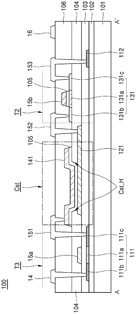
图4是沿图3的线A-A'截取的截面图。FIG. 4 is a cross-sectional view taken along line AA' of FIG. 3 .
图5是沿着图3的线B-B'截取的截面图。FIG. 5 is a cross-sectional view taken along line BB' of FIG. 3 .
图6示出了根据本发明的第二实施方案的对应于有机发光显示装置中的一个像素的等效电路的图。FIG. 6 shows a diagram corresponding to an equivalent circuit of one pixel in an organic light emitting display device according to a second embodiment of the present invention.
图7是示出了图6中示出的具有第一薄膜晶体管、第二薄膜晶体管和第三薄膜晶体管以及电容器的薄膜晶体管阵列基板的示例的图。FIG. 7 is a diagram showing an example of the thin film transistor array substrate shown in FIG. 6 having the first, second, and third thin film transistors and capacitors.
图8是沿图7的线C-C'截取的截面图。FIG. 8 is a cross-sectional view taken along line CC' of FIG. 7 .
图9是沿图7的线D-D'截取的截面图。FIG. 9 is a cross-sectional view taken along line DD' of FIG. 7 .
图10至图20是示出制造根据本发明的第二实施方案的薄膜晶体管阵列基板的方法的步骤的图。10 to 20 are diagrams illustrating steps of a method of manufacturing a thin film transistor array substrate according to a second embodiment of the present invention.
具体实施方式Detailed ways
将参照附图详细描述本发明的目的、特征和优点,以使本发明所涉及的本领域技术人员能够轻易地实践本发明的技术精神。此外,在本发明的下面的描述中,当确定对已知相关技术的详细描述会不必要地模糊本发明的主题时,将省略对已知相关技术的详细描述。在下文中,将参照附图详细描述本发明的优选实施方案。在附图中,使用相同的附图标记来指代相同或相似的部分。The objects, features and advantages of the present invention will be described in detail with reference to the accompanying drawings so that those skilled in the art to which the present invention pertains can easily practice the technical spirit of the present invention. Also, in the following description of the present invention, detailed descriptions of known related arts will be omitted when it is determined that they would unnecessarily obscure the subject matter of the present invention. Hereinafter, preferred embodiments of the present invention will be described in detail with reference to the accompanying drawings. In the drawings, the same reference numerals are used to designate the same or similar parts.
在下文中,将参照附图详细描述根据本发明的实施方案的薄膜晶体管阵列基板和具有该薄膜晶体管阵列基板的有机发光显示装置。Hereinafter, a thin film transistor array substrate and an organic light emitting display device having the thin film transistor array substrate according to embodiments of the present invention will be described in detail with reference to the accompanying drawings.
首先,参照图1,将说明根据本发明的一个实施方案的有机发光显示装置。First, referring to FIG. 1 , an organic light emitting display device according to an embodiment of the present invention will be explained.
图1是示出根据本发明的一个实施方案的有机发光显示装置的图。FIG. 1 is a diagram illustrating an organic light emitting display device according to one embodiment of the present invention.
如图1所示,根据本发明的实施方案的有机发光显示装置包括:具有多个像素PXL的显示面板10;用于驱动显示面板10的数据线14的数据驱动电路12;用于驱动显示面板10的第一扫描线15a和第二扫描线15b的栅极驱动电路13;以及用于控制数据驱动电路12和栅极驱动电路13的驱动定时的定时控制器11。As shown in FIG. 1 , an organic light emitting display device according to an embodiment of the present invention includes: a
尽管图1并未详细示出,但是显示面板10包括彼此面对彼此接合的一对基板(未示出);以及设置在这对基板之间的薄膜晶体管阵列和有机发光装置阵列。例如,这对基板中的一个可以是其上设置有薄膜晶体管阵列的薄膜晶体管阵列。并且,这对基板中的另一个可以是封装设置在薄膜晶体管阵列上的有机发光装置阵列的封装基板。Although not shown in detail in FIG. 1 , the
显示面板10的薄膜晶体管阵列基板包括:基板;在基板上设置成沿第一方向(图1中的左右方向)延伸的第一扫描线15a和第二扫描线15b;以及设置成沿第二方向(图1中的上下方向)延伸的数据线14。同时,对应于多个像素PXL的像素区域可以被定义为在第一扫描线15a和第二扫描线15b中的一个与数据线14之间的交叉区域。这些像素区域以矩阵的形式设置在实际显示图像的显示区域中。The thin film transistor array substrate of the
而且,显示面板10的薄膜晶体管阵列基板包括:用于向多个像素PXL提供第一驱动源极EVDD的第一电源线(未示出);以及用于提供低于第一驱动源极EVDD的第二驱动源极EVSS的第二电源线(未示出)。Moreover, the thin film transistor array substrate of the
定时控制器11根据显示面板10的分辨率重新布置从外部接收到的数字视频数据RGB,并且将重新布置的数字视频数据RGB’提供至数据驱动电路12。The
而且,定时控制器11基于各种定时信号例如垂直同步信号Vsync、水平同步信号Hsync、点时钟信号DCLK、数据使能信号DE等来提供用于控制数据驱动电路12的操作定时的数据控制信号DDC以及用于控制栅极驱动电路13的操作定时的栅极控制信号GDC。Also, the
数据驱动电路12基于数据控制信号DDC将重新布置的数字视频数据RGB'转换成模拟数据电压。并且,数据驱动电路12基于重新布置的数字视频数据RGB'在相应水平时段期间向相应水平线路的像素提供数据信号VDATA。The
栅极驱动电路13可以基于栅极控制信号GDC生成第一扫描信号SCAN1和第二扫描信号SCAN2。栅极驱动电路13可以向多条水平线顺序地提供第一扫描信号SCAN1和第二扫描信号SCAN2。同时,在每个水平时段期间,栅极驱动电路13向第一扫描线15a提供第一扫描信号SCAN1并且向第二扫描线15b提供第二扫描信号SCAN2。The
这种栅极驱动电路13可以根据板内栅极驱动器(GIP)方法设置在显示面板10的非显示区域中。Such a
接下来,将参照图2-5更加详细地描述根据本发明的第一实施方案的薄膜晶体管阵列基板。Next, the thin film transistor array substrate according to the first embodiment of the present invention will be described in more detail with reference to FIGS. 2-5.
图2是示出了根据本发明的第一实施方案的对应于有机发光显示装置中的一个像素的等效电路的图。图3是示出了图2中示出的具有第一薄膜晶体管、第二薄膜晶体管和第三薄膜晶体管以及电容器的薄膜晶体管阵列基板的示例的图。图4是沿图3的线A-A'截取的截面图。图5是沿着图3的线B-B'截取的截面图。FIG. 2 is a diagram showing an equivalent circuit corresponding to one pixel in an organic light emitting display device according to a first embodiment of the present invention. FIG. 3 is a diagram illustrating an example of the thin film transistor array substrate illustrated in FIG. 2 having first, second, and third thin film transistors and capacitors. FIG. 4 is a cross-sectional view taken along line AA' of FIG. 3 . FIG. 5 is a cross-sectional view taken along line BB' of FIG. 3 .
如图2所示,在根据本发明的第一实施方案的有机发光显示装置中,像素PXL中的每一个包括:有机发光装置OLED;向有机发光装置OLED提供驱动电流的第一薄膜晶体管T1;与第一薄膜晶体管T1的栅电极连接的电容器Cst和第二薄膜晶体管T2;以及与电容器Cst连接的第三薄膜晶体管T3。As shown in FIG. 2, in the organic light emitting display device according to the first embodiment of the present invention, each of the pixels PXL includes: an organic light emitting device OLED; a first thin film transistor T1 supplying a driving current to the organic light emitting device OLED; a capacitor Cst connected to the gate electrode of the first thin film transistor T1 and a second thin film transistor T2; and a third thin film transistor T3 connected to the capacitor Cst.
第一薄膜晶体管T1在提供第一驱动源极EVDD的第一电源线与提供第二驱动源极EVSS的第二电源线之间与有机发光装置OLED串联地连接。The first thin film transistor T1 is connected in series with the organic light emitting device OLED between a first power supply line providing a first driving source EVDD and a second power supply line providing a second driving source EVSS.
也就是说,第一薄膜晶体管T1的源电极和漏电极中的一个与提供第一驱动源极EVDD的第一电源线连接,而第一薄膜晶体管T1的源电极和漏电极中的另一个与有机发光装置OLED的阳极连接。并且,有机发光装置OLED的阴极与提供第二驱动源极EVSS的第二电源线连接。That is, one of the source electrode and the drain electrode of the first thin film transistor T1 is connected to the first power supply line providing the first driving source EVDD, and the other of the source electrode and the drain electrode of the first thin film transistor T1 is connected to the The anode connection of the organic light-emitting device OLED. Also, a cathode of the organic light emitting device OLED is connected to a second power line providing a second driving source EVSS.
电容器Cst连接在第一薄膜晶体管T1的栅电极与第三薄膜晶体管之间。电容器Cst由通过导通的第三薄膜晶体管T3提供的数据电压VDATA进行充电。The capacitor Cst is connected between the gate electrode of the first thin film transistor T1 and the third thin film transistor. The capacitor Cst is charged by the data voltage VDATA supplied through the turned-on third thin film transistor T3.
提供第二薄膜晶体管T2,以补偿第一薄膜晶体管T1的阈值电压。也就是说,提供第二薄膜晶体管T2,以防止提供给有机发光装置OLED的驱动电流受到第一薄膜晶体管T1的阈值电压的影响。The second thin film transistor T2 is provided to compensate the threshold voltage of the first thin film transistor T1. That is, the second thin film transistor T2 is provided to prevent the driving current supplied to the organic light emitting device OLED from being affected by the threshold voltage of the first thin film transistor T1.
第二薄膜晶体管T2可以连接在第一薄膜晶体管T1的源电极和漏电极中的与有机发光装置OLED连接的一个电极与第一薄膜晶体管T1的栅电极之间。并且,第二薄膜晶体管T2的栅电极与提供第二扫描信号SCAN2的第二扫描线15b连接。The second thin film transistor T2 may be connected between one of the source and drain electrodes of the first thin film transistor T1 connected to the organic light emitting device OLED and the gate electrode of the first thin film transistor T1. Also, the gate electrode of the second thin film transistor T2 is connected to the
也就是说,第二薄膜晶体管T2的源电极和漏电极中的一个与在第一薄膜晶体管T1的栅电极与电容器Cst之间的第一节点N1连接,第二薄膜晶体管T2的源电极和漏电极中的另一个与第一薄膜晶体管T1与有机发光装置OLED之间的第二节点N2连接。在基于第二扫描信号SCAN2而使第二薄膜晶体管T2导通时,其将第一节点N1与第二节点N2连接。That is, one of the source electrode and the drain electrode of the second thin film transistor T2 is connected to the first node N1 between the gate electrode of the first thin film transistor T1 and the capacitor Cst, and the source electrode and the drain electrode of the second thin film transistor T2 The other of the poles is connected to the second node N2 between the first thin film transistor T1 and the organic light emitting device OLED. When the second thin film transistor T2 is turned on based on the second scan signal SCAN2 , it connects the first node N1 to the second node N2 .
提供第三薄膜晶体管T3,以向电容器Cst和与电容器Cst连接的第一薄膜晶体管T1的栅电极提供用于驱动第一薄膜晶体管T1的数据信号。The third thin film transistor T3 is provided to supply a data signal for driving the first thin film transistor T1 to the capacitor Cst and the gate electrode of the first thin film transistor T1 connected to the capacitor Cst.
第三薄膜晶体管T3连接在提供数据信号VDATA的数据线14与电容器Cst之间。也就是说,第三薄膜晶体管T3的源电极和漏电极中的一个与提供数据信号VDATA的数据线14连接,而第三薄膜晶体管T3的源电极和漏电极中的另一个与电容器Cst连接。并且,第三薄膜晶体管T3的栅电极与提供第一扫描信号SCAN1的第一扫描线15a连接。在基于第一扫描信号SCAN1而使第三薄膜晶体管T3导通时,其向电容器Cst提供数据信号VDATA。The third thin film transistor T3 is connected between the
在如上所述的具有第一薄膜晶体管T1、第二薄膜晶体管T2和第三薄膜晶体管T3的薄膜晶体管阵列基板中,可以减小相应像素区域的尺寸,从而得到有机发光显示装置的高分辨率。在这种情况下,随着分配给相应薄膜晶体管的区域的减小,薄膜晶体管的一些特性可能劣化。例如,漏电流增加。In the thin film transistor array substrate having the first thin film transistor T1 , the second thin film transistor T2 and the third thin film transistor T3 as described above, the size of the corresponding pixel area can be reduced, thereby obtaining high resolution of the organic light emitting display device. In this case, as the area allocated to the corresponding thin film transistor decreases, some characteristics of the thin film transistor may be degraded. For example, leakage current increases.
作为又一示例,在第二薄膜晶体管T2中可能容易产生漏电流,这导致第一薄膜晶体管T1导通,并且出现有机发光装置OLED故障。As yet another example, a leakage current may be easily generated in the second thin film transistor T2, which causes the first thin film transistor T1 to be turned on, and failure of the organic light emitting device OLED occurs.
为了防止这种情况的发生,第二薄膜晶体管可以包括由下述氧化物半导体材料制成的有源层,该氧化物半导体材料与低温多晶硅半导体(LTPS)材料相比具有更优益的漏电流抑制特性。In order to prevent this, the second thin film transistor may include an active layer made of an oxide semiconductor material having a more favorable leakage current than a low temperature polysilicon semiconductor (LTPS) material. Inhibitory properties.
另一方面,为了加快对导通-关断切换进行响应的时间,第三薄膜晶体管T3可以包括由低温多晶硅半导体(LTPS)材料制成的有源层。On the other hand, in order to speed up the time to respond to the on-off switching, the third thin film transistor T3 may include an active layer made of a low temperature polysilicon semiconductor (LTPS) material.
并且,根据第一实施方案,与第三薄膜晶体管的情况相同,第一薄膜晶体管T1可以包括由LTPS制成的有源层。Also, according to the first embodiment, the first thin film transistor T1 may include an active layer made of LTPS as in the case of the third thin film transistor.
在这种情况下,为了简化流程,包括由LTPS制成的有源层的第一薄膜晶体管T1和第三薄膜晶体管T3可以实施为PMOS晶体管,而包括由氧化物半导体材料制成的有源层的第二薄膜晶体管T2可以实施为NMOS晶体管。In this case, in order to simplify the process, the first thin film transistor T1 and the third thin film transistor T3 including the active layer made of LTPS may be implemented as PMOS transistors, while the active layer including the oxide semiconductor material The second thin film transistor T2 can be implemented as an NMOS transistor.
如图3所示,根据本发明的第一实施方案的薄膜晶体管阵列基板100包括设置在相应像素区域中的第一薄膜晶体管T1、第二薄膜晶体管T2、第三薄膜晶体管T3和电容器Cst。As shown in FIG. 3, the thin film
薄膜晶体管阵列基板100还可以包括沿第一方向(图3中的左右方向)的第一扫描线15a和第二扫描线15b以及沿第二方向(图3中的上下方向)的数据线14和第一电源线16。The thin film
此外,薄膜晶体管阵列基板100还可以包括:用于将第三薄膜晶体管T3和电容器Cst连接的第一连接图案151;用于将第二薄膜晶体管T2与电容器Cst连接的第二连接图案152;以及用于将第一薄膜晶体管T1与第二薄膜晶体管T2连接的第三连接图案153。In addition, the thin film
第一薄膜晶体管T1的有源层112的两端分别与第一电源线16和第二薄膜晶体管T2连接。Both ends of the
第二薄膜晶体管T2的有源层131的两端分别与第一薄膜晶体管T1和电容器Cst连接。第二薄膜晶体管T2的栅电极由第二扫描线15b的与第二薄膜晶体管T2的有源层131的一部分交叠的部分制成。Both ends of the
第三薄膜晶体管T3的有源层111的两端分别与数据线14和电容器Cst连接。第三薄膜晶体管T3的栅电极由第一扫描线15a的与第三薄膜晶体管T3的有源层111的一部分交叠的部分制成。Both ends of the
电容器Cst包括彼此交叠的第一电容器电极121和第二电容器电极141。The capacitor Cst includes a
第一电容器电极121通过第二连接图案152与第二薄膜晶体管T2连接。并且,第一电容器电极121的与第一薄膜晶体管T1的有源层112的一部分交叠的部分用作第一薄膜晶体管T1的栅电极。因此,与第一薄膜晶体管T1的栅电极、第一电容器电极121和第二薄膜晶体管T2连接的第二连接图案152对应于图2中的第一节点N1。The
第二电容器电极141经由第一连接图案151与第三薄膜晶体管T3连接。The
电容器孔Cst_H设置在第一电容器电极121和第二电容器电极141彼此交叠的区域的一部分中。The capacitor hole Cst_H is disposed in a portion of a region where the
如图4所示,薄膜晶体管阵列基板100包括:覆盖基板101的表面的缓冲膜102;设置在缓冲膜102上的第三薄膜晶体管T3的有源层111;覆盖第三薄膜晶体管T3的有源层111的第一栅极绝缘膜103;设置在第一栅极绝缘膜103上的第三薄膜晶体管T3的栅电极15a;设置在第一栅极绝缘膜103上的并且与第三薄膜晶体管T3的栅电极15a间隔开的电容器Cst的第一电容器电极121;覆盖第三薄膜晶体管T3的栅电极15a和电容器Cst的第一电容器电极121的第二栅极绝缘膜104;对应于第一电容器电极121的一部分并且穿过第二栅极绝缘膜104的电容器孔Cst_H;设置在第二栅极绝缘膜104上的第二薄膜晶体管T2的有源层131;设置在覆盖第二栅极绝缘膜104的有源层131的一部分的中间绝缘膜105上的第二薄膜晶体管T2的栅电极15b;设置在中间绝缘膜105上的并且与第一电容器电极121交叠的电容器Cst的第二电容器电极141;覆盖第二薄膜晶体管T2的有源层131和栅电极15b以及电容器Cst的第二电容器电极142的层间绝缘膜106;设置在层间绝缘膜106上的数据线14和第一电源线16;以及第一连接图案151、第二连接图案152和第三连接图案153。As shown in FIG. 4 , the thin film transistor array substrate 100 includes: a buffer film 102 covering the surface of the substrate 101; an active layer 111 of the third thin film transistor T3 disposed on the buffer film 102; an active layer 111 covering the third thin film transistor T3; The first gate insulating film 103 of the layer 111; the gate electrode 15a of the third thin film transistor T3 provided on the first gate insulating film 103; The first capacitor electrode 121 of the capacitor Cst separated by the gate electrode 15a of the capacitor Cst; the second gate insulating film 104 covering the gate electrode 15a of the third thin film transistor T3 and the first capacitor electrode 121 of the capacitor Cst; corresponding to the first capacitor electrode 121 and pass through the capacitor hole Cst_H of the second gate insulating film 104; the active layer 131 of the second thin film transistor T2 provided on the second gate insulating film 104; The gate electrode 15b of the second thin film transistor T2 on the interlayer insulating film 105 that is part of the active layer 131; the second capacitor electrode 141 of the capacitor Cst that is provided on the interlayer insulating film 105 and overlaps the first capacitor electrode 121 ; the interlayer insulating film 106 covering the active layer 131 and the gate electrode 15b of the second thin film transistor T2 and the second capacitor electrode 142 of the capacitor Cst; the data line 14 and the first power supply line 16 provided on the interlayer insulating film 106 ; and the first connection pattern 151 , the second connection pattern 152 and the third connection pattern 153 .
换句话说,第三薄膜晶体管T3包括:设置在基板101或缓冲膜102上的有源层111;以及设置在第一栅极绝缘膜103上的并且由第一扫描线15a的与有源层111的一部分交叠的部分制成的栅电极15a。In other words, the third thin film transistor T3 includes: the
这里,设置在基板101或缓冲膜102上的有源层111可以由低温多晶硅(LTPS)材料制成。有源层包括:与栅电极15a交叠的沟道区111a;以及设置在沟道区111a两侧的源极区域111b和漏极区域111c。第三薄膜晶体管T3的源电极和漏电极分别对应于有源层111的源极区域111b和漏极区域111c。例如,有源层111的源极区域111b和漏极区域111c可以是由掺杂剂掺杂至浓度高于沟道区域111a的区域。Here, the
第三薄膜晶体管T3的源电极111b和漏电极111c中的一个(图4中的源电极111b)可以与设置在层间绝缘膜106上的数据线14连接,而第三薄膜晶体管T3的源电极111b和漏电极111c中的另一个(图4中的漏电极111c)可以通过设置在层间绝缘膜106上的第一连接图案151与电容器Cst的第二电容器电极141连接。One of the
电容器Cst设置在第一栅极绝缘膜102上,并且电容器Cst包括:与第一扫描线15a间隔开的第一电容器电极121;以及至少设置在中间绝缘膜105上的并且与第一电容器电极121交叠的第二电容器电极141。根据本发明的第一实施方案的电容器Cst包括对应于在第一电容器电极121与第二电容器电极141之间的交叠区域的一部分并且穿过第二栅极绝缘膜104的电容器孔Cst_H。The capacitor Cst is provided on the first
第一电容器电极121的一部分用作第一薄膜晶体管T1的栅电极,并且第二电容器电极141通过设置在层间绝缘膜106上的第一连接图案151与第三薄膜晶体管T3连接。A part of the
在第二电容器电极141下方的中间绝缘膜105设置在第二栅极绝缘膜104上。因此,第二电容器电极141的与电容器孔Cst_H对应的部分仅与中间绝缘膜105交叠,而剩余部分与第二栅极绝缘膜104和中间绝缘膜105交叠。也就是说,设置在第二电容器电极141下方的中间绝缘膜105的对应于电容器孔Cst_H的部分与第一电容器电极121和第二电容器电极141接触。The
类似地,仅中间绝缘膜105设置在第一电容器电极121与第二电容器电极141之间的交叠区域的对应于电容器孔Cst_H的部分中。同时,由第一电容器电极121和第二电容器电极141产生的电容器Cst的电容与第一电容器电极121和第二电容器电极141之间的间隔距离成反比。因此,当电容器孔Cst_H的在第一电容器电极121和第二电容器电极141之间仅设置有中间绝缘膜105的区域增加时,电容器Cst的电容可以增加,即使在有限区域中也是如此。Similarly, only the intermediate
第二薄膜晶体管T2包括:设置在覆盖第三薄膜晶体管T3的栅电极15a和电容器Cst的第一电容器电极121的第二栅极绝缘膜104上的有源层131;以及设置在覆盖有源层131的一部分的中间绝缘膜105上的并且由与有源层131的一部分交叠的第二扫描线15b的一部分制成的栅电极15b。The second thin film transistor T2 includes: an
这里,设置在第二栅极绝缘膜104上的有源层131可以由氧化物半导体材料制成。有源层131包括:与栅电极15b交叠的沟道区131a;以及设置在沟道区131a两侧的源极区域131b和漏极区域131c。第二薄膜晶体管T2的源电极和漏电极分别对应于有源层131的源极区域131b和漏极区域131c。例如,有源层131的源极区域131b和漏极区域131c可以是经过处理以与沟道区131a相比导电较多的区域。Here, the
第二薄膜晶体管T2的源电极131b和漏电极131c中的一个(图4中的源电极131b)可以与通过设置在层间绝缘膜106上的第二连接图案152与第一电容器电极121连接,而第二薄膜晶体管T2的源电极131b和漏电极131c中的另一个(图4中的漏电极131c)可以通过设置在层间绝缘膜106上的第三连接图案153与第一薄膜晶体管T1的有源层112连接。One of the
如图5所示,第一薄膜晶体管T1包括:设置在基板101或缓冲膜102上的有源层112;以及设置在第一栅极绝缘膜103上并且由与有源层112的一部分交叠的第一电容器电极121的一部分制成的栅电极121。As shown in FIG. 5, the first thin film transistor T1 includes: an
以与第三薄膜晶体管T3的有源层111类似的方式,第一薄膜晶体管T1的有源层112可以由LTPS制成。有源层112包括:与栅电极121交叠的沟道区112a;以及设置在沟道区112a两侧的源极区域112b和漏极区域112c。第一薄膜晶体管T2的源电极和漏电极分别对应于有源层112的源极区域112b和漏极区域112c。例如,有源层112的源极区域112b和漏极区域112c可以是由掺杂剂掺杂至浓度高于沟道区域112a的区域。In a similar manner to the
第一薄膜晶体管T1的源电极112b和漏电极112c中的一个(图5中的源电极112b)可以与设置在层间绝缘膜106上的第一电源线16连接,而第一薄膜晶体管T1的源电极112b和漏电极112c中的另一个(图5中的漏电极112c)可以通过设置在层间绝缘膜106上的第三连接图案153与第二薄膜晶体管T2连接。One of the
如上所述,根据本发明的第一实施方案,第一薄膜晶体管T1、第二薄膜晶体管T2和第三薄膜晶体管T3中的第三薄膜晶体管T3包括设置在基板101上的有源层111以及设置在覆盖有源层111的第一栅极绝缘膜103上的栅电极15a;并且第二薄膜晶体管T2包括设置在覆盖第三薄膜晶体管T3的栅电极15a的第二栅极绝缘膜104上的有源层131以及设置在覆盖有源层131的一部分的中间绝缘膜105上的栅电极15b。电容器Cst形成在设置在第一栅极绝缘膜103上的第一电容器电极121与设置在第二栅极绝缘膜104上的第二电容器电极141之间的交叠区域。As described above, according to the first embodiment of the present invention, the third thin film transistor T3 among the first thin film transistor T1, the second thin film transistor T2 and the third thin film transistor T3 includes the
以这种方式,可以通过设置在与第三薄膜晶体管T3的栅电极相同层上的第一电容器电极121和设置在与第二薄膜晶体管T2的栅电极相同层上的第二电容器电极141来实现电容器Cst。因此,由于可以在不添加单独的导电层的情况下实现电容器Cst,所以可以简化薄膜晶体管阵列基板100的结构。In this way, it can be realized by the
此外,根据本发明的第一实施方案,电容器Cst包括与在第一电容器电极121与第二电容器电极141之间的交叠区域的一部分对应的电容器孔Cst_H。同时,鉴于电容器孔Cst_H,所以在第一电容器电极121与第二电容器电极141之间仅设置有中间绝缘膜105。因此,电容器Cst的电容可以随着第一电容器电极121与第二电容器电极141之间的交叠区域的尺寸的增加而增加。因此,像素区域的尺寸减少,从而使电容器的电容下降最小化,即使在分配给电容器Cst的区域减小的情况下也是如此。因此,可以容易制造高分辨率的有机发光显示装置。In addition, according to the first embodiment of the present invention, the capacitor Cst includes the capacitor hole Cst_H corresponding to a portion of the overlapping region between the
同时,根据第一实施方案,为了防止因有机发光装置OLED故障而导致显示质量劣化,第一薄膜晶体管T1、第二薄膜晶体管T2和第三薄膜晶体管T3中的第二薄膜晶体管T2形成为包括由氧化物半导体材料制成的有源层131的结构。Meanwhile, according to the first embodiment, in order to prevent deterioration of display quality due to failure of the organic light emitting device OLED, the second thin film transistor T2 among the first thin film transistor T1, the second thin film transistor T2, and the third thin film transistor T3 is formed to include The structure of the
可替选地,与第二薄膜晶体管T2的情况相同,向有机发光装置OLED提供驱动电流的第一薄膜晶体管T1也可以形成为包括由氧化物半导体材料制成的有源层131的结构。Alternatively, as in the case of the second thin film transistor T2, the first thin film transistor T1 supplying a driving current to the organic light emitting device OLED may also be formed in a structure including the
接下来,将参照图6至图9描述根据第二实施方案的薄膜晶体管阵列基板。根据第二实施方案的薄膜晶体管阵列基板包括第一薄膜晶体管T1和第二薄膜晶体管T2,所述第一薄膜晶体管T1和第二薄膜晶体管T2以包括由氧化物半导体材料制成的有源层的结构形成。Next, a thin film transistor array substrate according to a second embodiment will be described with reference to FIGS. 6 to 9 . The thin film transistor array substrate according to the second embodiment includes a first thin film transistor T1 and a second thin film transistor T2 formed of an active layer made of an oxide semiconductor material. structure formed.
图6是示出了根据本发明的第二实施方案的对应于有机发光显示装置中的一个像素的等效电路的图。图7是示出了图6中示出的具有第一薄膜晶体管、第二薄膜晶体管和第三薄膜晶体管以及电容器的薄膜晶体管阵列基板的示例的图。图8是沿图7的线C-C'截取的截面图。图9是沿图7的线D-D'截取的截面图。FIG. 6 is a diagram showing an equivalent circuit corresponding to one pixel in an organic light emitting display device according to a second embodiment of the present invention. FIG. 7 is a diagram showing an example of the thin film transistor array substrate shown in FIG. 6 having the first, second, and third thin film transistors and capacitors. FIG. 8 is a cross-sectional view taken along line CC' of FIG. 7 . FIG. 9 is a cross-sectional view taken along line DD' of FIG. 7 .
如图6所示,根据本发明的第二实施方案的有机发光显示装置具有与图2所示的第一实施方案相同的结构,不同之处在于:对应于相应像素PXL的电容器Cst连接在第一节点N1与第二节点N2之间,并且第二薄膜晶体管T2连接在第一电源线16与第一薄膜晶体管T1之间的第三节点N3与第一节点N1之间。因此,下文将省略其重复性说明。As shown in FIG. 6, the organic light emitting display device according to the second embodiment of the present invention has the same structure as that of the first embodiment shown in FIG. Between the first node N1 and the second node N2, and the second thin film transistor T2 is connected between the
更具体地,根据第二实施方案,第一薄膜晶体管T1的源电极和漏电极中的一个与提供第一驱动源极EVDD的第一电源线连接,而第一薄膜晶体管T1的源电极和漏电极中的另一个与有机发光装置OLED的阳极连接。有机发光装置OLED的阴极与提供第二驱动源极EVSS的第二电源线连接。More specifically, according to the second embodiment, one of the source electrode and the drain electrode of the first thin film transistor T1 is connected to the first power supply line that provides the first driving source EVDD, and the source electrode and the drain electrode of the first thin film transistor T1 The other of the poles is connected to the anode of the organic light emitting device OLED. A cathode of the organic light emitting device OLED is connected to a second power line providing a second driving source EVSS.
电容器Cst连接在第一薄膜晶体管T1的源电极和漏电极中的与有机发光装置OLED连接的一个电极和第一薄膜晶体管T1的栅电极之间。也就是说,电容器Cst的第一电容器电极和第二电容器电极中的一个与第一薄膜晶体管T1的栅电极和第三薄膜晶体管T3之间的第一节点N1连接,而电容器Cst的第一电容器电极和第二电容器电极中的另一个与第一薄膜晶体管T1和有机发光装置OLED之间的第二节点N2连接。The capacitor Cst is connected between one of the source and drain electrodes of the first thin film transistor T1 connected to the organic light emitting device OLED and the gate electrode of the first thin film transistor T1. That is, one of the first capacitor electrode and the second capacitor electrode of the capacitor Cst is connected to the first node N1 between the gate electrode of the first thin film transistor T1 and the third thin film transistor T3, and the first capacitor electrode of the capacitor Cst The other of the electrode and the second capacitor electrode is connected to a second node N2 between the first thin film transistor T1 and the organic light emitting device OLED.
第二薄膜晶体管T2连接在第一薄膜晶体管T1的源电极和漏电极中的与第一电源线16连接的另一个电极和第一薄膜晶体管T1的栅电极之间。第二薄膜晶体管T2的栅电极与提供第二扫描信号SCAN2的第二扫描线15b连接。The second thin film transistor T2 is connected between the other electrode connected to the first
也就是说,第二薄膜晶体管T2的源电极和漏电极中的一个与第一薄膜晶体管T1的栅电极和第一电源线16之间的第三节点N3连接,而第二薄膜晶体管T2的源电极和漏电极中的另一个与第一节点N1连接。在基于第二扫描信号SCAN2而使第二薄膜晶体管T2导通时,其将第一节点N1与第三节点N3连接。That is, one of the source electrode and the drain electrode of the second thin film transistor T2 is connected to the third node N3 between the gate electrode of the first thin film transistor T1 and the first
第三薄膜晶体管T3连接在提供数据信号VDATA的数据线14和第一节点N1之间。也就是说,第三薄膜晶体管T3的源电极和漏电极中的一个与提供数据信号VDATA的数据线14连接,而第三薄膜晶体管T3的源电极和漏电极中的另一个与第一节点N1连接。第三薄膜晶体管T3的栅电极与提供第一扫描信号SCAN1的第一扫描线15a连接。在基于第一扫描信号SCAN1而导通第三薄膜晶体管T3时,其向第一节点N1提供数据信号VDATA。The third thin film transistor T3 is connected between the
如图7所示,根据本发明的第二实施方案的薄膜晶体管阵列基板100'包括设置在相应像素区域中的第一薄膜晶体管T1、第二薄膜晶体管T2、第三薄膜晶体管T3和电容器Cst。更具体地,与图3中的第一实施方案的不同之处在于:根据第二实施方案的薄膜晶体管T1的有源层132设置在第二薄膜晶体管T2的有源层131的相同层上。As shown in FIG. 7, the thin film transistor array substrate 100' according to the second embodiment of the present invention includes a first thin film transistor T1, a second thin film transistor T2, a third thin film transistor T3 and a capacitor Cst disposed in corresponding pixel regions. More specifically, the difference from the first embodiment in FIG. 3 is that the
薄膜晶体管阵列基板100'还可以包括沿第一方向(图7中的左右方向)的第一扫描线15a和第二扫描线15b;以及沿第二方向(图7中的上下方向)的数据线14和第一电源线16。The thin film transistor array substrate 100' may also include
此外,薄膜晶体管阵列基板100'还可以包括:将第二薄膜晶体管T2和第三薄膜晶体管T3与电容器Cst连接的第四连接图案154;以及将第一薄膜晶体管T1与电容器Cst连接的第五连接图案155。In addition, the thin film transistor array substrate 100' may further include: a
第一薄膜晶体管T1的有源层132的两端分别与第一电源线16和电容器Cst连接。Both ends of the
第二薄膜晶体管T2的有源层131的两端分别与第一电源线16和数据线14连接。第二薄膜晶体管T2的栅电极由第二扫描线15b的与第二薄膜晶体管T2的有源层131的一部分交叠的部分制成。Both ends of the
第三薄膜晶体管T3的有源层111的两端分别与数据线14和第二薄膜晶体管T2连接。第三薄膜晶体管T3的栅电极由第一扫描线15a的与第三薄膜晶体管T3的有源层111的一部分交叠的部分制成。Both ends of the
电容器Cst包括彼此交叠的第一电容器电极121和第二电容器电极141。The capacitor Cst includes a
第一电容器电极121通过第五连接图案155与在第一薄膜晶体管T1和有机发光装置OLED之间的第二节点(图6中的N2)连接。The
第二电容器电极141通过第四连接图案154与在第一薄膜晶体管T1的栅电极、第二薄膜晶体管T2和第三薄膜晶体管T3之间的第一节点(图6中的N1)连接。第二电容器电极141的与第一薄膜晶体管T1的有源层132的一部分交叠的部分用作第一薄膜晶体管T1的栅电极。The
电容器孔Cst_H设置在第一电容器电极121和第二电容器电极141彼此交叠的区域的一部分中。The capacitor hole Cst_H is disposed in a portion of a region where the
如图8所示,薄膜晶体管阵列基板100'包括:覆盖基板101的表面的缓冲膜102;设置在缓冲膜102上的第三薄膜晶体管T3的有源层111;覆盖第三薄膜晶体管T3的有源层111的第一栅极绝缘膜103;设置在第一栅极绝缘膜103上的第三薄膜晶体管T3的栅电极15a;设置在第一栅极绝缘膜103上的并且与第三薄膜晶体管T3的栅电极15a间隔开的电容器Cst的第一电容器电极121;覆盖第三薄膜晶体管T3的栅电极15a和电容器Cst的第一电容器电极121的第二栅极绝缘膜104;对应于第一电容器电极121的一部分并且穿过第二栅极绝缘膜104的电容器孔Cst_H;设置在中间绝缘膜105上的并且与第一电容器电极121交叠的电容器Cst的第二电容器电极141。As shown in FIG. 8, the thin film transistor array substrate 100' includes: a
如图9所示,薄膜晶体管阵列基板100'还包括:设置在第二栅极绝缘膜104上的第二薄膜晶体管T2的有源层131和第一薄膜晶体管T1的有源层132;设置在覆盖第二薄膜晶体管T2的有源层131的一部分的中间绝缘膜105上的第二薄膜晶体管T2的栅电极15b;以及设置在覆盖第一薄膜晶体管T1的有源层132的一部分的中间绝缘膜105上的第一薄膜晶体管T1的栅电极141。As shown in FIG. 9, the thin film transistor array substrate 100' further includes: the
此外,如图8和图9所示,薄膜晶体管阵列基板100'还包括:覆盖有源层131以及第二薄膜晶体管T2的栅电极15b和电容器Cst的第二电容器电极141的层间绝缘膜106;设置在层间绝缘膜106上的数据线14和第一电源线16;以及第四连接图案154和第五连接图案155。In addition, as shown in FIG. 8 and FIG. 9, the thin film transistor array substrate 100' further includes: an interlayer insulating
如图8和图9所示,根据第二实施方案100'的第二薄膜晶体管T2和第三薄膜晶体管T3具有与图4所示的第一实施方案100的第二薄膜晶体管T2和第三薄膜晶体管T3相同的结构。因此,下文将省略其重复性说明。As shown in FIG. 8 and FIG. 9, the second thin film transistor T2 and the third thin film transistor T3 according to the second embodiment 100' have the same characteristics as the second thin film transistor T2 and the third thin film transistor T2 and the third thin film transistor T2 of the
根据第二实施方案100',电容器Cst设置在第一栅极绝缘膜102上;并且电容器Cst包括:与第一扫描线15a间隔开的第一电容器电极121;以及至少设置在中间绝缘膜105上的并且与第一电容器电极121交叠的第二电容器电极141。根据本发明的第二实施方案的电容器Cst包括对应于第一电容器电极121和第二电容器电极141之间的交叠区域的一部分的并且穿过第二栅极绝缘膜104的电容器孔Cst_H。According to the second embodiment 100', the capacitor Cst is provided on the first
如图9所示,第一电容器电极121通过设置在层间绝缘膜106上的第五连接图案155与在第一薄膜晶体管T1和有机发光装置OLED之间的第二节点(图6中的N2)连接。As shown in FIG. 9, the
如图8所示,第二电容器电极141的一部分用作第一薄膜晶体管T1的栅电极。如图7和图8所示,第二电容器电极141经由设置在层间绝缘膜106上的第四连接图案154与在第二薄膜晶体管T2和第三薄膜晶体管T3之间的第一节点N1连接。As shown in FIG. 8, a part of the
与第一实施方案100的情况相同,根据第二实施方案100'的电容器Cst包括对应于第一电容器电极121和第二电容器电极141之间的交叠区域的一部分的并且穿过第二栅极绝缘膜104的电容器孔Cst_H。因此,可以增加电容器的电容,即使在有限区域中也是如此。As in the case of the
如图9所示,根据第二实施方案100',与第二薄膜晶体管T2的情况相同,第一薄膜晶体管T1包括:设置在覆盖第三薄膜晶体管T3的栅极电极15a和电容器Cst的第一电容器电极121的第二栅极绝缘膜104上的有源层132;以及设置在覆盖有源层132的一部分的中间绝缘膜105上的并且由与有源层132的一部分交叠的第二电容器电极141的一部分制成的栅电极141。As shown in FIG. 9, according to the second embodiment 100', as in the case of the second thin film transistor T2, the first thin film transistor T1 includes: the
以类似于第二薄膜晶体管T2的有源层131的方式,第一薄膜晶体管T1的有源层132可以由氧化物半导体材料制成。有源层132包括:与栅电极141交叠的沟道区132a;以及设置在沟道区132a两侧的源极区域132b和漏极区域132c。第一薄膜晶体管T1的源电极和漏电极分别对应于有源层132的源极区域132b和漏极区域132c。例如,有源层132的源极区域132b和漏极区域132c可以是经过处理以与沟道区132a相比导电较多的区域。In a manner similar to the
第一薄膜晶体管T1的源电极132b和漏电极132c中的一个(图9中的源电极132b)可以与设置在层间绝缘膜106上的第一电源线16连接,而第一薄膜晶体管T1的源电极132b和漏电极132c中的另一个(图9中的漏电极132c)可以通过设置在层间绝缘膜106上的第五连接图案155与电容器Cst的第一电容器电极121和有机发光装置(图6中的OLED)连接。One of the
如上所述,根据本发明的第二实施方案,向有机发光装置OLED提供驱动电流的第一薄膜晶体管T1可以形成为包括由氧化物半导体材料制成的有源层132的结构。因此,可以降低第一薄膜晶体管T1的电流-电压特性曲线图的斜率,从而容易控制相应像素PXL的灰度。As described above, according to the second embodiment of the present invention, the first thin film transistor T1 supplying a driving current to the organic light emitting device OLED may be formed in a structure including the
接下来,将参照图10至图20描述制造根据本发明的第二实施方案的薄膜晶体管阵列基板的方法。Next, a method of manufacturing a thin film transistor array substrate according to a second embodiment of the present invention will be described with reference to FIGS. 10 to 20 .
图10至图20是示出制造根据本发明的第二实施方案的薄膜晶体管阵列基板的方法的步骤的图。10 to 20 are diagrams illustrating steps of a method of manufacturing a thin film transistor array substrate according to a second embodiment of the present invention.
如图10和图11所示,在基板101的一个表面上设置缓冲膜102。然后,在缓冲膜102上设置第三薄膜晶体管的有源层111,并且设置第一栅极绝缘膜103以覆盖第三薄膜晶体管的有源层111。As shown in FIGS. 10 and 11 , a
随后,在第一栅极绝缘膜103上设置第一扫描线15a和第一电容器电极121。这里,第一扫描线15a的与第三薄膜晶体管的有源层111交叠的一部分用作第三薄膜晶体管的栅电极(图11中的15a)。Subsequently, the
然后,通过将第三薄膜晶体管的栅电极(图11中的15a)用作掩模,在第三薄膜晶体管的有源层111上进行掺杂剂注入工艺。因此,第三薄膜晶体管的有源层111具有包括与栅电极15a交叠的沟道区111a、以及设置在沟道区111a两侧的源极区域111b和漏极区域111c的结构。Then, a dopant implantation process is performed on the
如图12和图13所示,设置第二栅极绝缘膜104以覆盖第三薄膜晶体管的栅电极15a和第一电容器电极121。然后,设置穿过第二栅极绝缘膜104的电容器孔Cst_H,以露出第一电容器电极121的一部分。As shown in FIGS. 12 and 13 , a second
随后,在第二栅极绝缘膜104上设置第二薄膜晶体管的有源层131和第一薄膜晶体管的有源层132。Subsequently, the
接下来,对顺序地层叠在第二薄膜晶体管的有源层131和第一薄膜晶体管的有源层132上的绝缘膜(未示出)和导电层(未示出)作为一个整体进行图案化。Next, the insulating film (not shown) and the conductive layer (not shown) sequentially stacked on the
通过这样做,如图14和图15所示,提供了中间绝缘膜105、以及设置在中间绝缘膜上的第二扫描线15b和第二电容器电极141。By doing so, as shown in FIGS. 14 and 15 , the intermediate
这里,第二扫描线15b的与第二薄膜晶体管的有源层131交叠的部分用作第二薄膜晶体管的栅电极(图15中的15b)。Here, a portion of the
这里,第二电容器电极141的与第一薄膜晶体管的有源层132交叠的部分用作第一薄膜晶体管的栅电极(图15中的141)。Here, a portion of the
也就是说,如图15所示,提供了覆盖第二薄膜晶体管的有源层131的一部分的中间绝缘膜105和设置在中间绝缘膜上的第二薄膜晶体管的栅电极(图15中的15b);以及覆盖第一薄膜晶体管的有源层131的中间绝缘膜105和设置在中间绝缘膜上的第一薄膜晶体管的栅电极(图15中的141)。That is, as shown in FIG. 15 , an
如图16所示,通过将第一薄膜晶体管和第二薄膜晶体管的栅电极141和15b用作掩模,在第一薄膜晶体管和第二薄膜晶体管的有源层132和131上进行导电处理。因此,第一薄膜晶体管的有源层132具有包括与栅电极141交叠的沟道区132a以及设置在沟道区132a两侧的源极区域132b和漏极区域132c的结构。另外,第二薄膜晶体管的有源层131具有包括与栅电极15b交叠的沟道区131a以及设置在沟道区131a两侧的源极区域131b和漏极区域131c的结构。As shown in FIG. 16, conduction processing is performed on the
如图17和图18所示,提供层间绝缘膜106以覆盖第一薄膜晶体管和第二薄膜晶体管的栅电极141和15b;并且在层间绝缘膜106以及第一栅极绝缘膜103和第二栅极绝缘膜104中的至少一个绝缘膜(至少包括层间绝缘膜106)上进行图案化。As shown in FIGS. 17 and 18, an
结果,设置多个接触孔H1、H2、H3、H4、H5、H6,以对应于第一薄膜晶体管、第二薄膜晶体管和第三薄膜晶体管的有源层的源极区域和漏极区域。As a result, a plurality of contact holes H1, H2, H3, H4, H5, H6 are provided to correspond to the source and drain regions of the active layers of the first, second and third thin film transistors.
如图19和图20所示,在层间绝缘膜106上设置数据线14、第一电源线16、以及第四连接图案154和第五连接图案155。As shown in FIGS. 19 and 20 , the
如上描述的本发明不限于上述实施方案和附图;并且对于相关领域的普通技术人员来说明显的是,在不脱离本发明的技术精神的情况下,可以进行各种替换、修改和变化。The present invention as described above is not limited to the above embodiments and drawings; and it is obvious to those of ordinary skill in the related art that various substitutions, modifications and changes can be made without departing from the technical spirit of the present invention.
本申请还涉及以下技术方案。This application also relates to the following technical solutions.
1.一种薄膜晶体管阵列基板,其具有第一薄膜晶体管、与所述第一薄膜晶体管的栅电极连接的第二薄膜晶体管和电容器、以及与所述电容器连接的第三薄膜晶体管,其中,所述薄膜晶体管阵列基板包括:1. A thin film transistor array substrate, which has a first thin film transistor, a second thin film transistor connected to a gate electrode of the first thin film transistor and a capacitor, and a third thin film transistor connected to the capacitor, wherein the The thin film transistor array substrate includes:
设置在覆盖所述第三薄膜晶体管的有源层的第一栅极绝缘膜上的第一电容器电极;a first capacitor electrode disposed on the first gate insulating film covering the active layer of the third thin film transistor;
设置在覆盖所述第一电容器电极的第二栅极绝缘膜上的所述第二薄膜晶体管的有源层;an active layer of the second thin film transistor disposed on a second gate insulating film covering the first capacitor electrode;
设置在覆盖所述第二薄膜晶体管的有源层的一部分的中间绝缘膜上的所述第二薄膜晶体管的栅电极;以及a gate electrode of the second thin film transistor disposed on an interlayer insulating film covering a part of an active layer of the second thin film transistor; and
设置在所述中间绝缘膜上的并且与所述第一电容器电极交叠的所述电容器的第二电容器电极。A second capacitor electrode of the capacitor disposed on the intermediate insulating film and overlapping the first capacitor electrode.
2.根据项1所述的薄膜晶体管阵列基板,还包括:设置在所述第一栅极绝缘膜上的并且与所述第三薄膜晶体管的有源层的一部分交叠的所述第三薄膜晶体管的栅电极,其中,所述第一电容器电极与所述第三薄膜晶体管的所述栅电极间隔开。2. The thin film transistor array substrate according to item 1, further comprising: the third thin film provided on the first gate insulating film and overlapping with a part of the active layer of the third thin film transistor A gate electrode of a transistor, wherein the first capacitor electrode is spaced apart from the gate electrode of the third thin film transistor.
3.根据项1所述的薄膜晶体管阵列基板,还包括电容器孔,所述电容器孔对应于所述第一电容器电极和所述第二电容器电极彼此交叠的区域的一部分并且穿过所述第二栅极绝缘膜。3. The thin film transistor array substrate according to item 1, further comprising a capacitor hole corresponding to a part of an area where the first capacitor electrode and the second capacitor electrode overlap each other and passing through the first capacitor electrode. Two gate insulating films.
4.根据项1所述的薄膜晶体管阵列基板,其中,所述第一电容器电极和所述第二电容器电极中的一者与所述第一薄膜晶体管的栅电极连接。4. The thin film transistor array substrate according to item 1, wherein one of the first capacitor electrode and the second capacitor electrode is connected to a gate electrode of the first thin film transistor.
5.根据项1所述的薄膜晶体管阵列基板,其中,所述第一薄膜晶体管的有源层设置在与所述第三薄膜晶体管的所述有源层相同的层上;以及所述第一薄膜晶体管的所述栅电极设置在所述第一栅极绝缘膜上并且与所述第一电容器电极连接。5. The thin film transistor array substrate according to item 1, wherein the active layer of the first thin film transistor is disposed on the same layer as the active layer of the third thin film transistor; and the first thin film transistor The gate electrode of the thin film transistor is provided on the first gate insulating film and connected to the first capacitor electrode.
6.根据项4所述的薄膜晶体管阵列基板,其中,所述第一薄膜晶体管的有源层设置在所述第二栅极绝缘膜上,以及所述第一薄膜晶体管的所述栅电极设置在进一步覆盖所述第一薄膜晶体管的有源层的一部分的所述中间绝缘膜上并且与所述第二电容器电极连接。6. The thin film transistor array substrate according to item 4, wherein the active layer of the first thin film transistor is disposed on the second gate insulating film, and the gate electrode of the first thin film transistor is disposed On the interlayer insulating film further covering a part of the active layer of the first thin film transistor and connected to the second capacitor electrode.
7.根据项4所述的薄膜晶体管阵列基板,其中,所述第三薄膜晶体管的所述有源层由多晶硅半导体材料制成,以及所述第二薄膜晶体管的所述有源层由氧化物半导体材料制成。7. The thin film transistor array substrate according to item 4, wherein the active layer of the third thin film transistor is made of polysilicon semiconductor material, and the active layer of the second thin film transistor is made of oxide made of semiconductor material.
8.一种有机发光显示装置,其具有对应于相应的像素区域的有机发光装置、向所述有机发光装置提供驱动电流的第一薄膜晶体管、与所述第一薄膜晶体管的栅电极连接的电容器和第二薄膜晶体管、以及与所述电容器连接的第三薄膜晶体管,该有机发光显示装置包括:8. An organic light emitting display device having an organic light emitting device corresponding to a corresponding pixel region, a first thin film transistor supplying a driving current to the organic light emitting device, and a capacitor connected to a gate electrode of the first thin film transistor and the second thin film transistor, and the third thin film transistor connected to the capacitor, the organic light emitting display device includes:
设置在基板上的所述第三薄膜晶体管的有源层;The active layer of the third thin film transistor disposed on the substrate;
覆盖所述第三薄膜晶体管的所述有源层的第一栅极绝缘膜;a first gate insulating film covering the active layer of the third thin film transistor;
设置在所述第一栅极绝缘膜上的并且与所述第三薄膜晶体管的有源层的一部分交叠的所述第三薄膜晶体管的栅电极;a gate electrode of the third thin film transistor disposed on the first gate insulating film and overlapping a part of an active layer of the third thin film transistor;
设置在所述第一栅极绝缘膜上的并且与所述第三薄膜晶体管的所述栅电极间隔开的所述电容器的第一电容器电极;a first capacitor electrode of the capacitor disposed on the first gate insulating film and spaced apart from the gate electrode of the third thin film transistor;
覆盖所述第三薄膜晶体管的所述栅电极和所述电容器的所述第一电容器电极的第二栅极绝缘膜;a second gate insulating film covering the gate electrode of the third thin film transistor and the first capacitor electrode of the capacitor;
设置在所述第二栅极绝膜上的所述第二薄膜晶体管的有源层;an active layer of the second thin film transistor disposed on the second gate insulating film;
设置在覆盖所述第二薄膜晶体管的有源层的一部分的中间绝缘膜上的所述第二薄膜晶体管的栅电极;以及a gate electrode of the second thin film transistor disposed on an interlayer insulating film covering a part of an active layer of the second thin film transistor; and
设置在所述中间绝缘膜上的并且与所述第一电容器电极交叠的所述电容器的第二电容器电极。A second capacitor electrode of the capacitor disposed on the intermediate insulating film and overlapping the first capacitor electrode.
9.根据项8所述的有机发光显示装置,还包括电容器孔,所述电容器孔对应于所述第一电容器电极和所述第二电容器电极彼此交叠的区域的一部分并且穿过所述第二栅极绝缘膜。9. The organic light emitting display device according to item 8, further comprising a capacitor hole corresponding to a part of a region where the first capacitor electrode and the second capacitor electrode overlap each other and passing through the first capacitor electrode. Two gate insulating films.
10.根据项8所述的有机发光显示装置,其中,所述第一薄膜晶体管的所述有源层设置在与所述第三薄膜晶体管的所述有源层相同的层上;以及所述第一薄膜晶体管的所述栅电极设置在所述第一栅极绝缘膜上并且与所述第一电容器电极连接。10. The organic light emitting display device according to item 8, wherein the active layer of the first thin film transistor is disposed on the same layer as the active layer of the third thin film transistor; and the The gate electrode of the first thin film transistor is provided on the first gate insulating film and connected to the first capacitor electrode.
11.根据项10所述的有机发光显示装置,其中,所述第一薄膜晶体管的源电极和漏电极中的一者与第一电源线连接,而所述第一薄膜晶体管的所述源电极和所述漏电极中的另一者与所述有机发光装置连接,11. The organic light emitting display device according to
其中,所述第二薄膜晶体管中的源电极和漏电极中的一者与在所述电容器和所述第一薄膜晶体管的所述栅电极之间的第一节点连接,而所述第二薄膜晶体管中的所述源电极和所述漏电极中的另一者与在所述第一薄膜晶体管和所述有机发光装置之间的第二节点连接,wherein one of the source electrode and the drain electrode of the second thin film transistor is connected to a first node between the capacitor and the gate electrode of the first thin film transistor, and the second thin film transistor the other of the source electrode and the drain electrode of the transistors is connected to a second node between the first thin film transistor and the organic light emitting device,
其中,所述第三薄膜晶体管的源电极和漏电极中的一者与数据线连接,而所述第三薄膜晶体管的所述源电极和所述漏电极中的另一者与所述电容器的所述第二电容器电极连接,以及Wherein, one of the source electrode and the drain electrode of the third thin film transistor is connected to the data line, and the other of the source electrode and the drain electrode of the third thin film transistor is connected to the capacitor. The second capacitor electrode is connected, and
其中,所述有机发光装置的阳极与所述第二节点连接,而所述有机发光装置的阴极与第二电源线连接。Wherein, the anode of the organic light emitting device is connected to the second node, and the cathode of the organic light emitting device is connected to the second power line.
12.根据项8所述的有机发光显示装置,其中,所述第一薄膜晶体管的有源层设置在所述第二栅极绝缘膜上,以及所述第一薄膜晶体管的所述栅电极设置在进一步覆盖所述第一薄膜晶体管的有源层的一部分的所述中间绝缘膜上并且与所述第二电容器电极连接。12. The organic light emitting display device according to item 8, wherein the active layer of the first thin film transistor is disposed on the second gate insulating film, and the gate electrode of the first thin film transistor is disposed On the interlayer insulating film further covering a part of the active layer of the first thin film transistor and connected to the second capacitor electrode.
13.根据项12所述的有机发光显示装置,其中,所述第一薄膜晶体管的源电极和漏电极中的一者与第一电源线连接,而所述第一薄膜晶体管的所述源电极和所述漏电极中的另一者与所述有机发光装置连接,13. The organic light emitting display device according to
其中,所述电容器的所述第一电容器电极与在所述第一薄膜晶体管的所述栅电极和所述第三薄膜晶体管之间的第一节点连接,而所述电容器的所述第二电容器电极与在所述第一薄膜晶体管和所述有机发光装置之间的第二节点连接,Wherein, the first capacitor electrode of the capacitor is connected to a first node between the gate electrode of the first thin film transistor and the third thin film transistor, and the second capacitor electrode of the capacitor an electrode connected to a second node between the first thin film transistor and the organic light emitting device,
其中,所述第二薄膜晶体管的源电极和漏电极中的一者与所述第一节点连接,而所述第二薄膜晶体管的所述源电极和所述漏电极中的另一者与在所述第一电源线和所述第一薄膜晶体管之间的第三节点连接,Wherein, one of the source electrode and the drain electrode of the second thin film transistor is connected to the first node, and the other of the source electrode and the drain electrode of the second thin film transistor is connected to the a third node connection between the first power line and the first thin film transistor,
其中,所述第三薄膜晶体管的源电极和漏电极中的一者与数据线连接,而所述第三薄膜晶体管的所述源电极和所述漏电极中的另一者与所述第一节点连接,以及Wherein, one of the source electrode and the drain electrode of the third thin film transistor is connected to the data line, and the other of the source electrode and the drain electrode of the third thin film transistor is connected to the first node connections, and
其中,所述有机发光装置的阳极与所述第二节点连接,而所述有机发光装置的阴极与第二电源线连接。Wherein, the anode of the organic light emitting device is connected to the second node, and the cathode of the organic light emitting device is connected to the second power line.
14.根据项8所述的有机发光显示装置,还包括:覆盖所述第二薄膜晶体管的所述栅电极和所述第二电容器电极的层间绝缘膜,其中,所述第一电源线和所述数据线设置在所述层间绝缘膜上。14. The organic light emitting display device according to item 8, further comprising: an interlayer insulating film covering the gate electrode of the second thin film transistor and the second capacitor electrode, wherein the first power line and The data lines are disposed on the interlayer insulating film.
15.根据项8所述的有机发光显示装置,其中,所述第三薄膜晶体管的所述有源层由多晶硅半导体材料制成,以及所述第二薄膜晶体管的所述有源层由氧化物半导体材料制成。15. The organic light emitting display device according to item 8, wherein the active layer of the third thin film transistor is made of polysilicon semiconductor material, and the active layer of the second thin film transistor is made of oxide made of semiconductor material.
Claims (15)
Applications Claiming Priority (2)
| Application Number | Priority Date | Filing Date | Title |
|---|---|---|---|
| KR10-2017-0140194 | 2017-10-26 | ||
| KR1020170140194A KR102629437B1 (en) | 2017-10-26 | 2017-10-26 | Thin film transistor array substrateand organic light emitting display device comprising the same |
Publications (2)
| Publication Number | Publication Date |
|---|---|
| CN109727996A CN109727996A (en) | 2019-05-07 |
| CN109727996B true CN109727996B (en) | 2023-07-11 |
Family
ID=66244281
Family Applications (1)
| Application Number | Title | Priority Date | Filing Date |
|---|---|---|---|
| CN201811202004.2A Active CN109727996B (en) | 2017-10-26 | 2018-10-16 | Thin film transistor array substrate and organic light emitting display device having same |
Country Status (4)
| Country | Link |
|---|---|
| US (1) | US10615235B2 (en) |
| KR (1) | KR102629437B1 (en) |
| CN (1) | CN109727996B (en) |
| TW (1) | TWI690104B (en) |
Families Citing this family (14)
| Publication number | Priority date | Publication date | Assignee | Title |
|---|---|---|---|---|
| KR102435135B1 (en) * | 2018-02-05 | 2022-08-25 | 삼성디스플레이 주식회사 | Fingerprint sensing unit and display device including the same |
| KR102637791B1 (en) | 2018-02-13 | 2024-02-19 | 삼성디스플레이 주식회사 | Display apparatus |
| US11765935B2 (en) | 2019-07-04 | 2023-09-19 | Lg Display Co., Ltd. | Display apparatus |
| KR102612405B1 (en) * | 2019-07-09 | 2023-12-12 | 엘지디스플레이 주식회사 | Electronic device |
| KR102893872B1 (en) * | 2019-09-18 | 2025-12-03 | 삼성디스플레이 주식회사 | Display apparatus |
| KR102856056B1 (en) * | 2019-10-02 | 2025-09-05 | 삼성디스플레이 주식회사 | Display device |
| KR102871596B1 (en) * | 2019-11-19 | 2025-10-16 | 삼성디스플레이 주식회사 | Display device |
| KR102649412B1 (en) * | 2019-12-26 | 2024-03-21 | 엘지디스플레이 주식회사 | Thin film transistor array substrate and electronic device including the same |
| KR102950783B1 (en) * | 2020-02-24 | 2026-04-09 | 삼성디스플레이 주식회사 | Display panel |
| KR102260970B1 (en) * | 2020-03-26 | 2021-06-03 | 연세대학교 산학협력단 | Zero Bezel Display Apparatus Using Structure of Peripheral Circuit under Active Area, and Manufacturing Method |
| KR102861994B1 (en) | 2020-12-24 | 2025-09-18 | 엘지디스플레이 주식회사 | Display panel and display apparatus comprising the same, and method for manufacturing the same |
| CN113097232B (en) * | 2021-03-30 | 2024-06-11 | 合肥维信诺科技有限公司 | Display panel, method for manufacturing display panel, and display device |
| US12183280B2 (en) * | 2021-07-01 | 2024-12-31 | Universal Display Corporation | Means to reduce OLED transient response |
| US20240324286A1 (en) * | 2023-03-24 | 2024-09-26 | Samsung Display Co., Ltd. | Display apparatus |
Citations (2)
| Publication number | Priority date | Publication date | Assignee | Title |
|---|---|---|---|---|
| CN105304673A (en) * | 2014-06-11 | 2016-02-03 | 三星显示有限公司 | Organic light emitting diode display including sensors |
| CN106257677A (en) * | 2015-06-19 | 2016-12-28 | 乐金显示有限公司 | Thin film transistor base plate and the display device of this thin film transistor base plate of use |
Family Cites Families (6)
| Publication number | Priority date | Publication date | Assignee | Title |
|---|---|---|---|---|
| KR101152134B1 (en) | 2005-08-26 | 2012-06-15 | 삼성전자주식회사 | Organic light emitting display and manufacturing method thereof |
| WO2010044478A1 (en) * | 2008-10-16 | 2010-04-22 | Semiconductor Energy Laboratory Co., Ltd. | Light-emitting display device |
| KR102227474B1 (en) * | 2013-11-05 | 2021-03-15 | 삼성디스플레이 주식회사 | Thin film transistor array substrate, organic light-emitting display apparatus and manufacturing of the thin film transistor array substrate |
| KR102467574B1 (en) * | 2014-08-29 | 2022-11-18 | 엘지디스플레이 주식회사 | Thin Film Transistor Substrate And Display Using The Same |
| KR102567317B1 (en) * | 2015-12-29 | 2023-08-16 | 엘지디스플레이 주식회사 | Organic light emitting diode display device |
| US20170338252A1 (en) * | 2016-05-17 | 2017-11-23 | Innolux Corporation | Display device |
-
2017
- 2017-10-26 KR KR1020170140194A patent/KR102629437B1/en active Active
-
2018
- 2018-10-16 CN CN201811202004.2A patent/CN109727996B/en active Active
- 2018-10-25 US US16/170,925 patent/US10615235B2/en active Active
- 2018-10-26 TW TW107137927A patent/TWI690104B/en active
Patent Citations (2)
| Publication number | Priority date | Publication date | Assignee | Title |
|---|---|---|---|---|
| CN105304673A (en) * | 2014-06-11 | 2016-02-03 | 三星显示有限公司 | Organic light emitting diode display including sensors |
| CN106257677A (en) * | 2015-06-19 | 2016-12-28 | 乐金显示有限公司 | Thin film transistor base plate and the display device of this thin film transistor base plate of use |
Also Published As
| Publication number | Publication date |
|---|---|
| KR20190046414A (en) | 2019-05-07 |
| TWI690104B (en) | 2020-04-01 |
| KR102629437B1 (en) | 2024-01-24 |
| TW201924111A (en) | 2019-06-16 |
| CN109727996A (en) | 2019-05-07 |
| US10615235B2 (en) | 2020-04-07 |
| US20190131370A1 (en) | 2019-05-02 |
Similar Documents
| Publication | Publication Date | Title |
|---|---|---|
| CN109727996B (en) | Thin film transistor array substrate and organic light emitting display device having same | |
| US20240296794A1 (en) | Organic light-emitting display apparatus | |
| CN100541583C (en) | Display device and driving method thereof | |
| CN105225631B (en) | Show equipment | |
| EP3203521B1 (en) | Driving method for organic electroluminescent display device | |
| US10276638B2 (en) | Data driver and display device using the same | |
| US20060007072A1 (en) | Display device and driving method thereof | |
| US20200105192A1 (en) | Pixel of organic light emitting display device and organic light emitting display device having the same | |
| KR20160052943A (en) | Thin film transistor substrate | |
| CN106328051A (en) | Organic light emitting display apparatus | |
| US9972241B2 (en) | Display device | |
| US8847943B2 (en) | Organic light emitting display | |
| CN109727577B (en) | Organic light-emitting display device and method of driving the same | |
| JP2018013567A (en) | Display device | |
| CN113314574A (en) | Display device | |
| US7773055B2 (en) | Display device and driving method thereof | |
| EP3929904A1 (en) | Display device | |
| KR102551582B1 (en) | Organic light emitting display device | |
| US12010872B2 (en) | Display device | |
| JP2012137513A (en) | Signal processing device and display device | |
| US10482816B2 (en) | Method for driving display element, display device, and electronic device | |
| KR20190048557A (en) | Organic light emitting diode display device | |
| CN115881039B (en) | Pixel circuit and display device including the same | |
| JP6690614B2 (en) | Display device | |
| KR102536731B1 (en) | Organic light emitting display device |
Legal Events
| Date | Code | Title | Description |
|---|---|---|---|
| PB01 | Publication | ||
| PB01 | Publication | ||
| SE01 | Entry into force of request for substantive examination | ||
| SE01 | Entry into force of request for substantive examination | ||
| GR01 | Patent grant | ||
| GR01 | Patent grant |