CN110856384A - Electronic equipment shell, preparation method thereof and electronic equipment - Google Patents
Electronic equipment shell, preparation method thereof and electronic equipment Download PDFInfo
- Publication number
- CN110856384A CN110856384A CN201911061044.4A CN201911061044A CN110856384A CN 110856384 A CN110856384 A CN 110856384A CN 201911061044 A CN201911061044 A CN 201911061044A CN 110856384 A CN110856384 A CN 110856384A
- Authority
- CN
- China
- Prior art keywords
- texture
- electronic device
- dimensional texture
- bottom wall
- dimensional
- Prior art date
- Legal status (The legal status is an assumption and is not a legal conclusion. Google has not performed a legal analysis and makes no representation as to the accuracy of the status listed.)
- Granted
Links
Images




Classifications
-
- H—ELECTRICITY
- H05—ELECTRIC TECHNIQUES NOT OTHERWISE PROVIDED FOR
- H05K—PRINTED CIRCUITS; CASINGS OR CONSTRUCTIONAL DETAILS OF ELECTRIC APPARATUS; MANUFACTURE OF ASSEMBLAGES OF ELECTRICAL COMPONENTS
- H05K5/00—Casings, cabinets or drawers for electric apparatus
- H05K5/02—Details
Landscapes
- Engineering & Computer Science (AREA)
- Microelectronics & Electronic Packaging (AREA)
- Casings For Electric Apparatus (AREA)
Abstract
Description
技术领域technical field
本发明涉及电子设备技术领域,具体的,涉及电子设备壳体及其制备方法和电子设备。The present invention relates to the technical field of electronic equipment, and in particular, to an electronic equipment housing and a preparation method thereof, and electronic equipment.
背景技术Background technique
随着社会发展,科学的进步,人们对智能终端产品的外观审美的要求越来越高,目前主要流通的为2.5D壳体和3D壳体,外观效果主要从壳体色彩方面进行变化,如渐变色壳体等等,但随着技术的进一步发展,目前的壳体外观已经不能满足用户的审美要求,亟需外观效果更好、视觉冲击更强和更加时尚个性的壳体来满足用户审美要求。With the development of society and the progress of science, people have higher and higher requirements for the appearance and aesthetics of smart terminal products. At present, the main circulation is 2.5D shell and 3D shell, and the appearance effect mainly changes from the color of the shell, such as Gradient shells, etc., but with the further development of technology, the current shell appearance can no longer meet the aesthetic requirements of users, and a shell with better appearance effect, stronger visual impact and more fashionable personality is urgently needed to meet the user's aesthetics. Require.
发明内容SUMMARY OF THE INVENTION
本申请旨在至少在一定程度上解决相关技术中的技术问题之一。为此,本发明的一个目的在于提出一种立体感和视觉冲击力更强的电子设备壳体。The present application aims to solve one of the technical problems in the related art at least to a certain extent. Therefore, an object of the present invention is to provide an electronic device casing with stronger stereoscopic effect and visual impact.
在本申请的一个方面,本申请提供了一种电子设备壳体。根据本申请的实施例,该电子设备壳体包括:壳体本体,所述壳体本体包括底壁和与所述底壁相连的至少一个侧壁,所述底壁的内表面和所述侧壁的内表面中的至少之一上具有毫米级第一立体纹理,所述底壁的外表面为平面或弧面,所述侧壁的外表面为弧面,且所述底壁的外表面和所述侧壁的外表面中的至少之一上具有毫米级第二立体纹理。该电子设备壳体中,通过在内表面设置毫米级的立体纹理,用户肉眼观看可以直观看到强烈的立体效果,同时壳体外表面具有毫米级的第二立体纹理,肉眼观看和握持时用户均可感受到立体的纹理效果,该壳体能够同时从视觉和触觉上给予用户强烈的立体效果,满足时尚和个性化的要求,使得用户具有良好的使用体验。In one aspect of the present application, the present application provides an electronic device housing. According to an embodiment of the present application, the electronic device housing includes: a housing body comprising a bottom wall and at least one side wall connected to the bottom wall, an inner surface of the bottom wall and the side wall At least one of the inner surfaces of the walls has a millimeter-level first three-dimensional texture, the outer surface of the bottom wall is a plane or an arc surface, the outer surface of the side wall is an arc surface, and the outer surface of the bottom wall is an arc surface. and at least one of the outer surfaces of the side walls has a second three-dimensional texture of millimeter level. In the housing of the electronic device, by setting the millimeter-level three-dimensional texture on the inner surface, the user can intuitively see a strong three-dimensional effect when viewing with the naked eye. The three-dimensional texture effect can be felt, and the casing can give the user a strong three-dimensional effect from the visual and tactile aspects at the same time, which meets the requirements of fashion and personalization, and enables the user to have a good use experience.
在本申请的另一方面,本申请提供了一种制备电子设备壳体的方法。根据本申请的实施例,该方法包括:提供基材,所述基材具有相对设置的内表面和外表面;对所述基材进行第一CNC加工,所述第一CNC加工包括:从所述内表面一侧去除所述基材的一部分,以使所述基材形底壁和与所述底壁相连的至少一个侧壁,并在所述底壁的内表面和所述侧壁的内表面中的至少之一上形成毫米级第一立体纹理;对经过所述第一CNC加工的基材进行第二CNC加工,所述第二CNC加工包括:将所述基材与所述侧壁对应位置处的外表面加工成弧面;在所述外表面一侧去除所述基材的一部分,以在所述底壁的外表面和所述侧壁的外表面中的至少之一上形成毫米级第二立体纹理。该方法采用CNC加工进行,操作步骤简单,易于实现,自动化程度和加工精度高,且CNC加工技术成熟,易于实现工业化生产。In another aspect of the present application, the present application provides a method of manufacturing an electronic device housing. According to an embodiment of the present application, the method includes: providing a substrate, the substrate having oppositely disposed inner and outer surfaces; and performing a first CNC machining on the substrate, the first CNC machining including: A part of the base material is removed from one side of the inner surface, so that the base material-shaped bottom wall and at least one side wall connected to the bottom wall are separated from the inner surface of the bottom wall and the side wall. A millimeter-level first three-dimensional texture is formed on at least one of the inner surfaces; a second CNC processing is performed on the base material processed by the first CNC, and the second CNC processing includes: connecting the base material with the side The outer surface at the corresponding position of the wall is processed into an arc surface; a part of the base material is removed on one side of the outer surface, so as to be on at least one of the outer surface of the bottom wall and the outer surface of the side wall A millimeter-level second three-dimensional texture is formed. The method adopts CNC machining, the operation steps are simple, the realization is easy, the automation degree and machining accuracy are high, and the CNC machining technology is mature, and it is easy to realize industrialized production.
在本申请的另一个方面,本申请提供了一种电子设备。根据本申请的实施例,该电子设备包括前面所述的电子设备壳体,所述电子设备壳体的侧壁和底壁共同限定出容纳空间;显示屏,所述显示屏设置在所述容纳空间中。该电子设备具有立体感强、视觉冲击力强,能够满足用户对电子设备越来越高的外观审美要求,大大提高用户体验。In another aspect of the present application, the present application provides an electronic device. According to an embodiment of the present application, the electronic device includes the aforementioned electronic device housing, and the side walls and the bottom wall of the electronic device housing jointly define a accommodating space; a display screen, the display screen is arranged in the accommodating space in space. The electronic device has strong three-dimensional sense and strong visual impact, can meet the increasingly high aesthetic requirements of the user for the appearance of the electronic device, and greatly improves the user experience.
附图说明Description of drawings
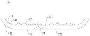
图1是本申请一个实施例的电子设备壳体的结构示意图。FIG. 1 is a schematic structural diagram of an electronic device casing according to an embodiment of the present application.
图2是本申请另一个实施例的电子设备壳体的结构示意图。FIG. 2 is a schematic structural diagram of an electronic device casing according to another embodiment of the present application.
图3是图2中圆圈部分的局部放大示意图。FIG. 3 is a partial enlarged schematic view of the circled portion in FIG. 2 .
图4是本申请另一个实施例的电子设备壳体的结构示意图。FIG. 4 is a schematic structural diagram of an electronic device casing according to another embodiment of the present application.
图5是本申请一个实施例的电子设备壳体的结构示意图。FIG. 5 is a schematic structural diagram of an electronic device casing according to an embodiment of the present application.
图6是本申请另一个实施例的电子设备壳体的结构示意图。FIG. 6 is a schematic structural diagram of an electronic device casing according to another embodiment of the present application.
图7是本申请另一个实施例的电子设备壳体的结构示意图。FIG. 7 is a schematic structural diagram of an electronic device casing according to another embodiment of the present application.
图8是本申请另一个实施例的电子设备壳体的结构示意图。FIG. 8 is a schematic structural diagram of an electronic device casing according to another embodiment of the present application.
图9是本申请另一个实施例的电子设备壳体的结构示意图。FIG. 9 is a schematic structural diagram of an electronic device casing according to another embodiment of the present application.
图10是本申请另一个实施例的电子设备壳体的结构示意图。FIG. 10 is a schematic structural diagram of an electronic device casing according to another embodiment of the present application.
图11是本申请另一个实施例的电子设备壳体的结构示意图。FIG. 11 is a schematic structural diagram of an electronic device casing according to another embodiment of the present application.
图12是本申请另一个实施例的电子设备壳体的结构示意图。FIG. 12 is a schematic structural diagram of an electronic device casing according to another embodiment of the present application.
图13是本申请一个实施例的电子设备的结构示意图。FIG. 13 is a schematic structural diagram of an electronic device according to an embodiment of the present application.
具体实施方式Detailed ways
下面详细描述本发明的实施例。下面描述的实施例是示例性的,仅用于解释本发明,而不能理解为对本发明的限制。实施例中未注明具体技术或条件的,按照本领域内的文献所描述的技术或条件或者按照产品说明书进行。所用试剂或仪器未注明生产厂商者,均为可以通过市购获得的常规产品。Embodiments of the present invention are described in detail below. The embodiments described below are exemplary, only for explaining the present invention, and should not be construed as limiting the present invention. If no specific technique or condition is indicated in the examples, the technique or condition described in the literature in the field or the product specification is used. The reagents or instruments used without the manufacturer's indication are conventional products that can be obtained from the market.
在本申请的一个方面,本申请提供了一种电子设备壳体。根据本申请的实施例,参照图1和图2,该电子设备壳体包括:壳体本体10,所述壳体本体10包括底壁12和与所述底壁12相连的至少一个侧壁14,所述底壁12的内表面121和所述侧壁14的内表面141中的至少之一上具有毫米级第一立体纹理22,所述底壁12的外表面122为平面(参照图1)或弧面(参照图2),所述侧壁14的外表面142为弧面;且所述底壁12的外表面122和所述侧壁14的外表面142中的至少之一上具有毫米级第二立体纹理24。该电子设备壳体中,通过在内表面设置毫米级的立体纹理,用户肉眼观看可以直观看到强烈的立体效果,同时壳体外表面具有毫米级的第二立体纹理,肉眼观看和握持时用户均可感受到立体的纹理效果,该壳体能够同时从视觉和触觉上给予用户强烈的立体效果,满足时尚和个性化的要求,使得用户具有良好的使用体验。In one aspect of the present application, the present application provides an electronic device housing. According to an embodiment of the present application, referring to FIGS. 1 and 2 , the electronic device housing includes: a
需要说明的是,本文中采用的描述方式“毫米级第一立体纹理”和“毫米级第二立体纹理”是指第一立体纹理和第二立体纹理的至少一个维度上的尺寸为毫米级,即至少一个维度上的尺寸为可以为0.1mm~10mm,例如可以立体纹理的高度或立体纹理的线宽为毫米级,也可以是立体纹理的高度或立体纹理的线宽均为毫米级。It should be noted that the description methods "millimeter-level first three-dimensional texture" and "millimeter-level second three-dimensional texture" used in this document mean that the dimensions of the first three-dimensional texture and the second three-dimensional texture in at least one dimension are in the millimeter level, That is, the size in at least one dimension may be 0.1 mm to 10 mm, for example, the height of the three-dimensional texture or the line width of the three-dimensional texture may be in the order of millimeters, or the height of the three-dimensional texture or the line width of the three-dimensional texture may be in the order of millimeters.
可以理解,壳体本体的具体材质没有特别限制,只要是可以适用于电子设备壳体的材质即可。具体的,壳体本体的材质可以为玻璃、陶瓷等,由此,材料来源广泛,价格较低,且不会有信号屏蔽问题,能够满足5G的使用要求。一些具体实施例中,壳体本体的材质为玻璃。由此,材料来源广泛,光学性能好,且成本较低。It can be understood that the specific material of the casing body is not particularly limited, as long as it is a material suitable for the casing of an electronic device. Specifically, the material of the housing body can be glass, ceramics, etc. Therefore, the material has a wide range of sources, the price is low, and there is no signal shielding problem, which can meet the use requirements of 5G. In some specific embodiments, the material of the housing body is glass. As a result, the material source is wide, the optical performance is good, and the cost is low.
可以理解,上述第一立体纹理和第二立体纹理可以各自独立的包括多个纹理面,至少一部分所述纹理面相交,且两个所述纹理面相交处的R角大于等于0.2mm,具体可以为0.5mm~3mm,更具体可以为0.2mm、0.3mm、0.4mm、0.5mm、0.8mm、1.0mm、1.2mm、1.3mm、1.8mm、2.0mm、2.2mm、2.5mm、2.8mm、3.0mm等。由此,第一立体纹理和第二立体纹理具有明显的棱角结构,外观效果更加立体,视觉冲击感更强,且更加时尚、个性,能够带给用户更好的使用体验。It can be understood that the above-mentioned first three-dimensional texture and second three-dimensional texture may each independently include a plurality of texture surfaces, at least a part of the texture surfaces intersect, and the R angle at the intersection of the two texture surfaces is greater than or equal to 0.2 mm. 0.5mm~3mm, more specifically 0.2mm, 0.3mm, 0.4mm, 0.5mm, 0.8mm, 1.0mm, 1.2mm, 1.3mm, 1.8mm, 2.0mm, 2.2mm, 2.5mm, 2.8mm, 3.0 mm etc. Therefore, the first three-dimensional texture and the second three-dimensional texture have obvious angular structures, the appearance effect is more three-dimensional, the visual impact is stronger, and it is more fashionable and individual, which can bring a better user experience.
需要说明的是,本文中的描述方式“R角”是指两个纹理面相交处的过渡圆弧的半径,具体示意图参照图3;另外,“各自独立的”是指互不影响,例如第一立体纹理和第二立体纹理可以各自独立的满足某一参数范围,是指第一立体纹理和第二立体纹理的该参数的具体取值互不影响,即第一立体纹理的该参数的具体数值和第二立体纹理的该参数的具体数值可以相同也可以不同。It should be noted that the description method "R angle" in this paper refers to the radius of the transition arc at the intersection of the two texture surfaces, and the specific schematic diagram refers to Fig. 3; A three-dimensional texture and a second three-dimensional texture can independently satisfy a certain parameter range, which means that the specific values of the parameter of the first three-dimensional texture and the second three-dimensional texture do not affect each other, that is, the specific value of the parameter of the first three-dimensional texture The value and the specific value of the parameter of the second three-dimensional texture may be the same or different.
可以理解,参照图1、图2和图4,上述第一立体纹理22和第二立体纹理24可以向壳体本体10外部凸起,也可以向所述壳体本体10内部凹陷,具体可以根据想要实现的外观效果进行选择。一些具体实施例中,参照图1和图2,所述第一立体纹理22向所述壳体本体10内部凹陷,所述第二立体纹理24向所述壳体本体10外部凸起。由此,壳体本体的内表面更加易于与电子设备的其他组件进行组装,提高了空间利用率,利于实现电子设备的小型化,同时可以避免组装过程中对立体纹理造成磕碰、刮擦等损伤,成品良率更高,外观效果更佳,外表面的第二立体纹理向外凸起,用户触摸时可以直接感受到立体效果,该壳体在视觉和触觉上同时实现强烈的立体感,给用户以更新鲜、冲击感更强的使用体验,满足时尚和个性化要求。It can be understood that, referring to FIGS. 1 , 2 and 4 , the above-mentioned first three-
具体的,第一立体纹理和第二立体纹理的具体形状和尺寸没有特别限制,可以根据实际需要灵活选择。一些具体实施例中,参照图5和图6,所述第一立体纹理和第二立体纹理各自独立的包括直线条纹、曲线条纹、几何图形和不规则图形中的至少一种。由此,可以实现更加丰富和美观的外观效果,提高用户体验。Specifically, the specific shapes and sizes of the first three-dimensional texture and the second three-dimensional texture are not particularly limited, and can be flexibly selected according to actual needs. In some specific embodiments, referring to FIG. 5 and FIG. 6 , the first three-dimensional texture and the second three-dimensional texture independently include at least one of linear stripes, curved stripes, geometric figures and irregular figures. Thereby, a richer and more beautiful appearance effect can be achieved, and the user experience can be improved.
具体的,每条第一立体纹理和每条第二立体纹理的截面形状也可以是多种多样的,一些具体实施例中,每条第一立体纹理的截面和每条第二立体纹理的截面的形状可以各自独立的为三角形(参照图1、图2和图4)、梯形(参照图7)、矩形(参照图8)、割圆(参照图9)以及其他平面几何图形和不规则图形(参照图10)。由此,可以提供更加丰富多样的立体外观。需要说明的是,割圆是指圆形被一直线切割后形成的两个部分中的一个,即圆形被一直线切割后形成两个部分,其中每个部分均可以称为割圆。Specifically, the cross-sectional shape of each first three-dimensional texture and each second three-dimensional texture can also be varied. In some specific embodiments, the cross-section of each first three-dimensional texture and the cross-section of each second three-dimensional texture The shapes can be independently triangles (refer to Figures 1, 2 and 4), trapezoids (refer to Figure 7), rectangles (refer to Figure 8), secant circles (refer to Figure 9) and other planar geometric figures and irregular figures (refer to Fig. 10). Thereby, a more diverse three-dimensional appearance can be provided. It should be noted that a secant circle refers to one of two parts formed by cutting a circle by a straight line, that is, two parts are formed after a circle is cut by a straight line, and each part can be called a secant circle.
具体的,该电子设备壳体中的第一立体纹理和第二立体纹理的具体尺寸为毫米级(0.1mm~10mm),在该尺寸范围内肉眼可以直观看到强烈的立体感,且与可见光波长差异比较明显,基本不会产生干涉、衍射等光学作用,可以让用户直接感受到强烈的立体视觉冲击。具体的,第一立体纹理的高度可以小于等于第二立体纹理的高度。具体的,位于内表面的第一立体纹理主要用于肉眼观察立体效果,较小的纹理高度即可有效被肉眼识别,易于加工,利于电子设备中其他部件的组装,同时利于减低壳体本体的厚度,使得壳体更轻薄,而位于外表面的第二立体纹理同时用于给予用户立体的视觉冲击和在用户握持电子设备时可以直接感受到立体外观效果,为了保证较明显的立体触感,可以使得第二立体纹理的高度相对较大。Specifically, the specific size of the first three-dimensional texture and the second three-dimensional texture in the casing of the electronic device is millimeter level (0.1mm-10mm). The wavelength difference is relatively obvious, and there is basically no optical effect such as interference and diffraction, which allows users to directly experience a strong stereoscopic visual impact. Specifically, the height of the first three-dimensional texture may be less than or equal to the height of the second three-dimensional texture. Specifically, the first three-dimensional texture located on the inner surface is mainly used to observe the three-dimensional effect with the naked eye, and a small texture height can be effectively recognized by the naked eye, which is easy to process, facilitates the assembly of other components in the electronic device, and helps to reduce the thickness of the housing body. Thickness makes the shell thinner and lighter, and the second three-dimensional texture on the outer surface is used to give users a three-dimensional visual impact and directly feel the three-dimensional appearance effect when the user holds the electronic device. In order to ensure a more obvious three-dimensional touch, The height of the second three-dimensional texture can be made relatively large.
一些具体的实施例中,所述第一立体纹理的高度H1可以为0.1~1mm(具体如0.1mm、0.2mm、0.3mm、0.4mm、0.5mm、0.6mm、0.7mm、0.8mm、0.9mm、1.0mm等);第二立体纹理的高度H2可以为0.5~2.5mm,具体可以为0.5~2mm,更具体可以为0.5mm、0.6mm、0.7mm、0.8mm、0.9mm、1.0mm、1.1mm、1.2mm、1.3mm、1.4mm、1.5mm、1.6mm、1.7mm、1.8mm、1.9mm、2.0mm等等。In some specific embodiments, the height H1 of the first three-dimensional texture may be 0.1-1 mm (specifically, such as 0.1 mm, 0.2 mm, 0.3 mm, 0.4 mm, 0.5 mm, 0.6 mm, 0.7 mm, 0.8 mm, 0.9 mm) , 1.0mm, etc.); the height H2 of the second three-dimensional texture can be 0.5-2.5mm, specifically 0.5-2mm, more specifically 0.5mm, 0.6mm, 0.7mm, 0.8mm, 0.9mm, 1.0mm, 1.1 mm, 1.2mm, 1.3mm, 1.4mm, 1.5mm, 1.6mm, 1.7mm, 1.8mm, 1.9mm, 2.0mm, etc.
需要说明的是,本文中采用的描述方式“立体纹理的高度”是指立体纹理向壳体本体内部凹陷的深度或者立体纹理向壳体本体外部凸起的高度,具体的,以底壁的内表面上设有立体纹理为例说明,当立体纹理向壳体本体内部凹陷时,凹陷的立体纹理以外的部分构成凸起部分,该凸起部分的内表面位于一个平面或一个弧面内(参照图1、图2和图4中虚线部分所示),立体纹理的高度即是指立体纹理相对上述平面或弧面向壳体本体内部凹陷的深度。同理,当立体纹理向壳体本体外部凸起时,凸起的立体纹理以外的部分构成凹陷部分,该凹陷部分位于一个平面或一个弧面内,立体纹理的高度即是指立体纹理相对上述平面或弧面向壳体本体外部凸起的高度。It should be noted that the description method used in this article "the height of the three-dimensional texture" refers to the depth of the three-dimensional texture concave to the inside of the shell body or the height of the three-dimensional texture to the outside of the shell body. There is a three-dimensional texture on the surface as an example to illustrate that when the three-dimensional texture is concave to the inside of the housing body, the part other than the concave three-dimensional texture constitutes a convex part, and the inner surface of the convex part is located in a plane or an arc surface (refer to 1, 2 and 4), the height of the three-dimensional texture refers to the depth of the hollow of the three-dimensional texture relative to the above-mentioned plane or arc surface inside the housing body. In the same way, when the three-dimensional texture protrudes to the outside of the shell body, the part other than the raised three-dimensional texture constitutes a concave part, and the concave part is located in a plane or an arc surface, and the height of the three-dimensional texture refers to the three-dimensional texture relative to the above The height at which the plane or arc protrudes toward the exterior of the housing body.
一些具体的实施例中,所述第一立体纹理的线宽W1和所述第二立体纹理的线宽W2各自独立的可以大于等于1mm,具体可以为1~10mm,更具体可以为1mm、2mm、3mm、4mm、5mm、6mm、7mm、8mm、9mm、10mm等。需要说明的是,第一立体纹理和第二立体纹理可以各自独立的包括多条纹理线,每条纹理线的宽度均在上述范围内,但其宽度可以相同,也可以不同。在该范围内,立体效果更强,外观效果更好,且易于进行加工,如果过小,则加工难度加大,纹理可能会崩坏、损伤,如果过大会不利于实现更多样化的外观效果。In some specific embodiments, the line width W1 of the first three-dimensional texture and the line width W2 of the second three-dimensional texture may independently be greater than or equal to 1 mm, specifically may be 1-10 mm, more specifically may be 1 mm, 2 mm , 3mm, 4mm, 5mm, 6mm, 7mm, 8mm, 9mm, 10mm, etc. It should be noted that the first three-dimensional texture and the second three-dimensional texture may independently include multiple texture lines, and the width of each texture line is within the above range, but the widths may be the same or different. Within this range, the three-dimensional effect is stronger, the appearance effect is better, and it is easy to process. If it is too small, the processing difficulty will increase, and the texture may be collapsed and damaged. If it is too large, it is not conducive to achieving a more diverse appearance. Effect.
可以理解,第一立体纹理和第二立体纹理可以各自独立的是连续的纹理(参照图6),也可以是间隔设置的多个纹理(参照图7)。一些具体实施例中,第一立体纹理和第二立体纹理可以各自独立的包括多个间隔设置的子纹理,相邻两个所述子纹理之间的距离L大于等于1mm,具体可以为1~15mm,更具体可以为1mm、2mm、3mm、4mm、5mm、6mm、7mm、8mm、9mm、10mm、11mm、12mm、13mm、14mm、15mm等。由此,可以根据需要灵活设置纹理间距,实现丰富多样的外观效果。It can be understood that the first three-dimensional texture and the second three-dimensional texture may be independent continuous textures (refer to FIG. 6 ), or may be multiple textures arranged at intervals (refer to FIG. 7 ). In some specific embodiments, the first three-dimensional texture and the second three-dimensional texture may independently include a plurality of sub-textures arranged at intervals, and the distance L between two adjacent sub-textures is greater than or equal to 1 mm, and may be 1 to 1 mm. 15mm, more specifically 1mm, 2mm, 3mm, 4mm, 5mm, 6mm, 7mm, 8mm, 9mm, 10mm, 11mm, 12mm, 13mm, 14mm, 15mm, etc. As a result, the texture spacing can be flexibly set as required to achieve a variety of appearance effects.
一些具体实施例中,参照图2,所述壳体本体10的最大厚度D1可以为3~10mm(具体可以为3mm、4mm、5mm、6mm、7mm、8mm、9mm、10mm等),而所述壳体本体10的最小厚度D2可以大于等于0.4mm(具体可以为0.4mm、0.5mm、0.6mm、0.7mm、0.8mm、0.9mm、1mm、2mm、3mm、4mm、5mm、6mm、7mm、8mm、9mm等)。由此,在实现立体纹理的同时,可以既保证电子设备壳体使用时的强度要求,又符合轻薄化的发展趋势。In some specific embodiments, referring to FIG. 2 , the maximum thickness D1 of the
需要说明的是,由于底壁和侧壁的至少之一的内表面和外表面上均具有立体纹理,即内表面和外表面均为非平坦的,所以壳体本体的不同位置的厚度可以是不同的(非等厚的),上述壳体本体的最大厚度就是指壳体本体厚度最大的位置处的厚度,而壳体本体的最小厚度就是指壳体本体厚度最小的位置处的厚度。另一些实施例中,壳体本体的不同位置的厚度可以是大致相同的(等厚的),参照图11,即壳体本体内表面的立体纹理和壳体本体外表面的立体纹理的凸起和凹陷的相互配合,内表面的立体纹理向壳体本体外部凸起,则相应位置处的外表面的立体纹理就向壳体本体内部凹陷,反之内表面的立体纹理向壳体本体内部凹陷,则相应位置处的外表面的立体纹理就向壳体本体外部凸起。It should be noted that, since at least one of the bottom wall and the side wall has a three-dimensional texture on the inner surface and the outer surface, that is, the inner surface and the outer surface are both non-planar, the thickness of the shell body at different positions can be Different (non-equal thickness), the maximum thickness of the housing body refers to the thickness at the position where the thickness of the housing body is the largest, and the minimum thickness of the housing body refers to the thickness at the position where the thickness of the housing body is the smallest. In other embodiments, the thicknesses of different positions of the housing body may be approximately the same (equal thickness), referring to FIG. 11 , that is, the three-dimensional texture of the inner surface of the housing body and the protrusions of the three-dimensional texture on the outer surface of the housing body In cooperation with the depression, the three-dimensional texture of the inner surface protrudes to the outside of the shell body, then the three-dimensional texture of the outer surface at the corresponding position is concave to the inside of the shell body, and the three-dimensional texture of the inner surface is concave to the inside of the shell body. Then the three-dimensional texture of the outer surface at the corresponding position protrudes to the outside of the housing body.
另外,第一立体纹理和第二立体纹理在壳体本体厚度方向上的正投影可以至少部分不重叠,由此第一立体纹理和第二立体纹理均可被用户直接看到,能够更加丰富壳体的外观。一些具体实施例中,第一立体纹理和第二立体纹理在壳体本体厚度方向上的正投影可以完全不重叠,也可以部分重叠部分不重叠。进一步的,第一立体纹理和第二立体纹理还可以共同叠加构成一个完成的装饰图案,例如可以第一立体纹理形成星星的图案,而第二第一纹理形成月亮、太阳等星球的图案,两者叠加共同构成天空的装饰图案等。In addition, the orthographic projections of the first three-dimensional texture and the second three-dimensional texture in the thickness direction of the shell body may not overlap at least partially, so that both the first three-dimensional texture and the second three-dimensional texture can be directly seen by the user, which can enrich the shell body appearance. In some specific embodiments, the orthographic projections of the first three-dimensional texture and the second three-dimensional texture in the thickness direction of the casing body may not overlap at all, or may partially overlap and partially overlap. Further, the first three-dimensional texture and the second three-dimensional texture can also be superimposed together to form a completed decorative pattern. For example, the first three-dimensional texture can form a pattern of stars, and the second first texture can form a pattern of planets such as the moon and the sun. They are superimposed together to form decorative patterns of the sky, etc.
可以理解,参照图12,该电子设备壳体还可以包括:装饰膜片30,所述装饰膜片30设置在所述底壁12和所述侧壁14的内表面上。由此,可以通过装饰膜片实现不同颜色、不同图案等等的外观装饰效果,使得壳体的外观更加丰富多样、绚烂夺目,更好的满足用户的审美要求。It can be understood that, referring to FIG. 12 , the electronic device housing may further include: a
可以理解,装饰膜片可以为多层结构,具体可以包括颜色层、纹理层、盖底油墨层和必要的粘结层等,也可以包括基材膜片,上述颜色层、纹理层、盖底油墨层等预先形成在基材膜片上,然后贴合在壳体的内表面上。具体的装饰膜片结构、材质等可以更具实际需要的外观效果进行选择,在此不再过多赘述。It can be understood that the decorative film can be a multi-layer structure, and can specifically include a color layer, a texture layer, a cover bottom ink layer and a necessary adhesive layer, etc., and can also include a substrate film, the above-mentioned color layer, texture layer, cover bottom An ink layer and the like are formed on the base film in advance, and then attached to the inner surface of the casing. The specific decorative film structure, material, etc. can be selected according to the actual needs of the appearance effect, which will not be repeated here.
在本申请的另一方面,本申请提供了一种制备电子设备壳体的方法。根据本申请的实施例,该方法包括:提供基材,所述板材具有相对设置的内表面和外表面;对所述基材进行第一CNC加工,所述第一CNC加工包括:从所述内表面一侧去除所述基材的一部分,以使所述基材形底壁和与所述底壁相连的至少一个侧壁,并在所述底壁的内表面和所述侧壁的内表面中的至少之一上形成毫米级立体纹理;对经过所述第一CNC加工的基材进行第二CNC加工,所述第二CNC加工包括:将所述基材与所述侧壁对应位置处的外表面加工成弧面;在所述外表面一侧去除所述基材的一部分,以在所述底壁的外表面和所述侧壁的外表面中的至少之一上形成毫米级第二立体纹理。该方法采用CNC加工进行,操作步骤简单,易于实现,自动化程度和加工精度高,且CNC加工技术成熟,易于实现工业化生产。In another aspect of the present application, the present application provides a method of manufacturing an electronic device housing. According to an embodiment of the present application, the method includes: providing a base material, the sheet material having oppositely disposed inner and outer surfaces; and performing a first CNC machining on the base material, the first CNC machining including: starting from the A part of the substrate is removed from one side of the inner surface, so that the substrate-shaped bottom wall and at least one side wall connected to the bottom wall are separated from the inner surface of the bottom wall and the inner side of the side wall. A millimeter-level three-dimensional texture is formed on at least one of the surfaces; a second CNC processing is performed on the base material processed by the first CNC, and the second CNC processing includes: corresponding positions of the base material and the side walls At least one of the outer surface of the bottom wall and the outer surface of the side wall is formed by removing a part of the base material on one side of the outer surface to form a millimeter scale The second three-dimensional texture. The method adopts CNC machining, the operation steps are simple, the realization is easy, the automation degree and machining accuracy are high, and the CNC machining technology is mature, and it is easy to realize industrialized production.
可以理解,第二CNC加工过程中,从外表面一侧去除基材的一部分以形成第二立体纹理的步骤和将所述基材与所述侧壁对应位置处的外表面加工成弧面的步骤没有先后顺序的限制,可以先去除基材的一部分以形成第二立体纹理,然后再将侧壁对应的外表面加工为弧面,也可以先将侧壁对应的外表面加工为弧面,然后再去除基材的一部分以形成第二立体纹理,具体可以根据需要灵活调整。It can be understood that, in the second CNC machining process, the step of removing a part of the base material from the outer surface side to form the second three-dimensional texture and processing the outer surface of the base material at the position corresponding to the side wall into an arc surface. The steps are not limited in sequence. A part of the base material can be removed first to form a second three-dimensional texture, and then the outer surface corresponding to the side wall can be processed into an arc surface, or the outer surface corresponding to the side wall can be processed into an arc surface first. Then, a part of the substrate is removed to form a second three-dimensional texture, which can be flexibly adjusted as required.
可以理解,上述方法还可以包括:将所述基材与所述底壁对应位置处的外表面加工成弧面。由此,可以形成具有3D结构的壳体。具体的,该步骤可以在形成第二立体纹理之前进行,也可以和形成第二立体纹理同步进行。It can be understood that the above method may further include: processing the outer surface of the base material at the position corresponding to the bottom wall into an arc surface. Thereby, a casing having a 3D structure can be formed. Specifically, this step may be performed before the formation of the second three-dimensional texture, or may be performed simultaneously with the formation of the second three-dimensional texture.
具体的,所述第二CNC加工之前,将经过所述第一CNC加工的基材固定在治具上,所述治具与所述基材接触的表面上具有与所述第一立体纹理互补的仿形立体纹理,以使得所述第一立体纹理可以配合固定在所述仿形立体纹理中。由此,可以更好的将形成有第一立体纹理的基材固定,且仿形立体纹理可以很好的和第一立体纹理配合,不会损伤第一立体纹理。Specifically, before the second CNC processing, the substrate processed by the first CNC is fixed on a jig, and the surface of the jig in contact with the substrate has a complementary texture to the first three-dimensional texture The profiling three-dimensional texture, so that the first three-dimensional texture can be fixed in the profiling three-dimensional texture. In this way, the substrate formed with the first three-dimensional texture can be better fixed, and the profiling three-dimensional texture can be well matched with the first three-dimensional texture without damaging the first three-dimensional texture.
需要说明的,本文中采用的描述方式“与所述第一立体纹理互补的仿形立体纹理”是指仿形立体纹理与第一立体纹理互补,具体是指在基材和治具对应的位置上(即治具固定基材上,治具和基材需要接触的位置),第一立体纹理和仿形纹理的尺寸以及凸起和凹陷的趋势是大约相同的,当基材固定到治具上时,立体纹理可以恰好放置在仿形纹理中,两者接触的位置处两者之间几乎没有间隙。It should be noted that the description method used in this article "the profiling three-dimensional texture complementary to the first three-dimensional texture" means that the profiling three-dimensional texture is complementary to the first three-dimensional texture, and specifically refers to the position corresponding to the substrate and the fixture. On (i.e. the position where the jig and the substrate need to be in contact with the substrate on the fixture), the dimensions of the first three-dimensional texture and the profiling texture, as well as the protruding and concave trends are about the same, when the substrate is fixed to the jig , the solid texture can be placed right in the profiling texture with little to no gap between the two where they touch.
具体的,CNC加工的具体步骤和参数等均可以根据想要实现的结构和图案灵活调整,在此不再一一赘述。而本领域技术人员可以理解,该方法可以用于制备前面所述的电子设备壳体,涉及的特征和优点可以与前文相应描述一致,在此不再一一描述。Specifically, the specific steps and parameters of CNC machining can be flexibly adjusted according to the structure and pattern to be realized, and will not be repeated here. However, those skilled in the art can understand that the method can be used to prepare the aforementioned electronic device housing, and the involved features and advantages can be consistent with the aforementioned corresponding descriptions, and will not be described one by one here.
一个具体实施例中,可以先提供平板基材,然后通过CNC加工在基材的内表面上加工出第一立体纹理,然后将得到的基材固定吸附在具有上述仿形立体纹理的治具(具体可以为治具中具有仿形纹理的3D底座上)上,进一步通过CNC加工将侧壁对应的外表面加工为弧面,并在底壁对应的外表面上形成第二立体纹理。In a specific embodiment, a flat substrate can be provided first, then a first three-dimensional texture can be processed on the inner surface of the substrate by CNC machining, and then the obtained substrate is fixed and adsorbed on a jig ( Specifically, on the 3D base with profiling texture in the fixture), the outer surface corresponding to the side wall is further processed into an arc surface by CNC machining, and a second three-dimensional texture is formed on the outer surface corresponding to the bottom wall.
可以理解,当壳体本体为等厚时,也可以利用模具对基材进行成型处理制得,具体可以采用具有目标纹理形状的模具,在一定温度和压力条件下对基材进行成型,以在基材的内表面和外表面形成立体纹理的同时,基材的边沿弯曲,形成壳体本体的侧壁。It can be understood that when the shell body is of the same thickness, the base material can also be formed by using a mold. Specifically, a mold with a target texture shape can be used to shape the base material under certain temperature and pressure conditions, so as to form the base material. When the inner surface and the outer surface of the base material form a three-dimensional texture, the edge of the base material is bent to form the side wall of the casing body.
在本申请的另一个方面,本申请提供了一种电子设备。根据本申请的实施例,参照图13,该电子设备包括前面所述的电子设备壳体100,所述电子设备壳体的侧壁和底壁共同限定出容纳空间;显示屏200,所述显示屏200设置在所述容纳空间中。该电子设备具有立体感强、视觉冲击力强、且握感舒适的外观效果,能够满足用户对电子设备越来越高的外观审美要求,大大提高用户体验。In another aspect of the present application, the present application provides an electronic device. According to an embodiment of the present application, referring to FIG. 13 , the electronic device includes the aforementioned
可以理解,该电子设备的具体种类没有特别限制,可以为任何常规电子设备,例如包括但不限于手机、平板电脑、游戏机、可穿戴设备、生活电器等的功能。另外,本领域技术人员也可以理解,除了前面所述的电子设备壳体,该电子设备还可以包括常规电子设备必备的其他结构和部件,以手机为例,还可以包括触控模组、照相模组、指纹识别模组、声音处理系统、电池、主板、储存器以及必要的电路结构等等,在此不再一一赘述。It can be understood that the specific type of the electronic device is not particularly limited, and can be any conventional electronic device, for example, including but not limited to functions of mobile phones, tablet computers, game consoles, wearable devices, and household appliances. In addition, those skilled in the art can also understand that, in addition to the aforementioned electronic device housing, the electronic device may also include other structures and components necessary for conventional electronic devices. Taking a mobile phone as an example, it may also include a touch module, The camera module, fingerprint identification module, sound processing system, battery, mainboard, storage and necessary circuit structure, etc., will not be repeated here.
在本说明书的描述中,参考术语“一个实施例”、“一些实施例”、“示例”、“具体示例”、或“一些示例”等的描述意指结合该实施例或示例描述的具体特征、结构、材料或者特点包含于本发明的至少一个实施例或示例中。在本说明书中,对上述术语的示意性表述不必须针对的是相同的实施例或示例。而且,描述的具体特征、结构、材料或者特点可以在任一个或多个实施例或示例中以合适的方式结合。此外,在不相互矛盾的情况下,本领域的技术人员可以将本说明书中描述的不同实施例或示例以及不同实施例或示例的特征进行结合和组合。In the description of this specification, description with reference to the terms "one embodiment," "some embodiments," "example," "specific example," or "some examples", etc., mean specific features described in connection with the embodiment or example , structure, material or feature is included in at least one embodiment or example of the present invention. In this specification, schematic representations of the above terms are not necessarily directed to the same embodiment or example. Furthermore, the particular features, structures, materials or characteristics described may be combined in any suitable manner in any one or more embodiments or examples. Furthermore, those skilled in the art may combine and combine the different embodiments or examples described in this specification, as well as the features of the different embodiments or examples, without conflicting each other.
尽管上面已经示出和描述了本发明的实施例,可以理解的是,上述实施例是示例性的,不能理解为对本发明的限制,本领域的普通技术人员在本发明的范围内可以对上述实施例进行变化、修改、替换和变型。Although the embodiments of the present invention have been shown and described above, it should be understood that the above-mentioned embodiments are exemplary and should not be construed as limiting the present invention. Embodiments are subject to variations, modifications, substitutions and variations.
Claims (15)
Priority Applications (4)
| Application Number | Priority Date | Filing Date | Title |
|---|---|---|---|
| CN201911061044.4A CN110856384B (en) | 2019-11-01 | 2019-11-01 | Electronic device casing and preparation method thereof, and electronic device |
| US17/780,012 US20220408570A1 (en) | 2019-11-01 | 2020-06-02 | Electronic device housing, manufacturing method therefor, and electronic device |
| PCT/CN2020/093964 WO2021082443A1 (en) | 2019-11-01 | 2020-06-02 | Electronic device housing and manufacturing method therefor, and electronic device |
| EP20880557.2A EP4050869B1 (en) | 2019-11-01 | 2020-06-02 | Electronic device housing and manufacturing method therefor, and electronic device |
Applications Claiming Priority (1)
| Application Number | Priority Date | Filing Date | Title |
|---|---|---|---|
| CN201911061044.4A CN110856384B (en) | 2019-11-01 | 2019-11-01 | Electronic device casing and preparation method thereof, and electronic device |
Publications (2)
| Publication Number | Publication Date |
|---|---|
| CN110856384A true CN110856384A (en) | 2020-02-28 |
| CN110856384B CN110856384B (en) | 2021-06-25 |
Family
ID=69599599
Family Applications (1)
| Application Number | Title | Priority Date | Filing Date |
|---|---|---|---|
| CN201911061044.4A Active CN110856384B (en) | 2019-11-01 | 2019-11-01 | Electronic device casing and preparation method thereof, and electronic device |
Country Status (1)
| Country | Link |
|---|---|
| CN (1) | CN110856384B (en) |
Cited By (10)
| Publication number | Priority date | Publication date | Assignee | Title |
|---|---|---|---|---|
| CN112045945A (en) * | 2020-08-14 | 2020-12-08 | Oppo广东移动通信有限公司 | Battery cover, shell assembly, electronic equipment and forming die |
| WO2021082443A1 (en) * | 2019-11-01 | 2021-05-06 | Oppo广东移动通信有限公司 | Electronic device housing and manufacturing method therefor, and electronic device |
| CN112839120A (en) * | 2020-12-28 | 2021-05-25 | 北京小米移动软件有限公司 | Electronic equipment |
| CN113115529A (en) * | 2021-04-07 | 2021-07-13 | 维沃移动通信有限公司 | Machining method of shell, shell and electronic equipment |
| CN113292232A (en) * | 2021-06-18 | 2021-08-24 | Oppo广东移动通信有限公司 | Manufacturing method of electronic device shell, electronic device shell and electronic device |
| CN113461318A (en) * | 2021-06-28 | 2021-10-01 | Oppo广东移动通信有限公司 | Preparation method of shell, display assembly and electronic device |
| CN114051344A (en) * | 2021-11-05 | 2022-02-15 | Oppo广东移动通信有限公司 | Shell, preparation method thereof and electronic equipment |
| CN114667002A (en) * | 2020-12-24 | 2022-06-24 | Oppo广东移动通信有限公司 | Electronic equipment shell, manufacturing method thereof, mold and electronic equipment |
| CN114697427A (en) * | 2020-12-31 | 2022-07-01 | Oppo广东移动通信有限公司 | Shell, manufacturing method thereof and electronic equipment |
| KR102940889B1 (en) * | 2021-09-23 | 2026-03-20 | 삼성전자주식회사 | Electronic device including housing |
Citations (4)
| Publication number | Priority date | Publication date | Assignee | Title |
|---|---|---|---|---|
| US20120244321A1 (en) * | 2011-03-25 | 2012-09-27 | Hon Hai Precision Industry Co., Ltd. | Method for manufacturing a product shell and structure |
| CN206149655U (en) * | 2016-09-12 | 2017-05-03 | 潮州三环(集团)股份有限公司 | Portable electronic equipment apron and portable electronic equipment |
| CN107835276A (en) * | 2017-12-08 | 2018-03-23 | 南昌欧菲光科技有限公司 | Flexible cover plate of electronic equipment and preparation method thereof and electronic equipment |
| CN109561607A (en) * | 2017-09-25 | 2019-04-02 | 广东长盈精密技术有限公司 | Electronic equipment casing, casing processing method and device |
-
2019
- 2019-11-01 CN CN201911061044.4A patent/CN110856384B/en active Active
Patent Citations (4)
| Publication number | Priority date | Publication date | Assignee | Title |
|---|---|---|---|---|
| US20120244321A1 (en) * | 2011-03-25 | 2012-09-27 | Hon Hai Precision Industry Co., Ltd. | Method for manufacturing a product shell and structure |
| CN206149655U (en) * | 2016-09-12 | 2017-05-03 | 潮州三环(集团)股份有限公司 | Portable electronic equipment apron and portable electronic equipment |
| CN109561607A (en) * | 2017-09-25 | 2019-04-02 | 广东长盈精密技术有限公司 | Electronic equipment casing, casing processing method and device |
| CN107835276A (en) * | 2017-12-08 | 2018-03-23 | 南昌欧菲光科技有限公司 | Flexible cover plate of electronic equipment and preparation method thereof and electronic equipment |
Cited By (13)
| Publication number | Priority date | Publication date | Assignee | Title |
|---|---|---|---|---|
| WO2021082443A1 (en) * | 2019-11-01 | 2021-05-06 | Oppo广东移动通信有限公司 | Electronic device housing and manufacturing method therefor, and electronic device |
| CN112045945A (en) * | 2020-08-14 | 2020-12-08 | Oppo广东移动通信有限公司 | Battery cover, shell assembly, electronic equipment and forming die |
| CN114667002A (en) * | 2020-12-24 | 2022-06-24 | Oppo广东移动通信有限公司 | Electronic equipment shell, manufacturing method thereof, mold and electronic equipment |
| CN114667002B (en) * | 2020-12-24 | 2024-11-15 | Oppo广东移动通信有限公司 | Electronic device housing, manufacturing method thereof, mold, and electronic device |
| CN112839120A (en) * | 2020-12-28 | 2021-05-25 | 北京小米移动软件有限公司 | Electronic equipment |
| CN112839120B (en) * | 2020-12-28 | 2023-01-10 | 北京小米移动软件有限公司 | Electronic equipment |
| CN114697427A (en) * | 2020-12-31 | 2022-07-01 | Oppo广东移动通信有限公司 | Shell, manufacturing method thereof and electronic equipment |
| CN113115529A (en) * | 2021-04-07 | 2021-07-13 | 维沃移动通信有限公司 | Machining method of shell, shell and electronic equipment |
| CN113292232A (en) * | 2021-06-18 | 2021-08-24 | Oppo广东移动通信有限公司 | Manufacturing method of electronic device shell, electronic device shell and electronic device |
| CN113461318A (en) * | 2021-06-28 | 2021-10-01 | Oppo广东移动通信有限公司 | Preparation method of shell, display assembly and electronic device |
| CN113461318B (en) * | 2021-06-28 | 2023-01-31 | Oppo广东移动通信有限公司 | Preparation method of shell, display assembly and electronic device |
| KR102940889B1 (en) * | 2021-09-23 | 2026-03-20 | 삼성전자주식회사 | Electronic device including housing |
| CN114051344A (en) * | 2021-11-05 | 2022-02-15 | Oppo广东移动通信有限公司 | Shell, preparation method thereof and electronic equipment |
Also Published As
| Publication number | Publication date |
|---|---|
| CN110856384B (en) | 2021-06-25 |
Similar Documents
| Publication | Publication Date | Title |
|---|---|---|
| CN110856384A (en) | Electronic equipment shell, preparation method thereof and electronic equipment | |
| US8675862B1 (en) | Method and apparatus of a certain cell phone case with a universal decorative pattern layer | |
| CN111016415B (en) | Texture transfer master mold, plate and preparation method, texture transfer sub-mold, shell, electronic equipment | |
| US11877411B2 (en) | Electronic device including rear plate and method for manufacturing same | |
| CN110845126B (en) | Method for manufacturing electronic equipment casing, electronic equipment casing and electronic equipment | |
| CN107454225B (en) | Three-dimensional cambered surface glass, mobile phone cover, manufacturing method of three-dimensional cambered surface glass and mobile phone cover and mobile phone | |
| US20210037126A1 (en) | Electronic device and electronic device housing structure | |
| KR102639402B1 (en) | An electronic device comprising a patterned housing | |
| CN107879638A (en) | Bend glass sheet material, preparation method, composite reagent and mobile terminal | |
| KR20200076802A (en) | Decoration film and electronic deive including the same | |
| CN117957922A (en) | Electronic device housing and electronic device including the electronic device housing | |
| CN108900658B (en) | Housing, electronic device, and method for manufacturing housing | |
| CN114280711B (en) | Transparent plate, manufacturing method thereof, shell and mobile terminal | |
| CN210297785U (en) | Electronic equipment housings and electronic equipment | |
| EP4050869B1 (en) | Electronic device housing and manufacturing method therefor, and electronic device | |
| CN110868819A (en) | Preparation method of casing, casing and electronic device | |
| US10200516B2 (en) | Interlocking ceramic and optical members | |
| CN110769100A (en) | Electronic equipment shell, preparation method thereof and electronic equipment | |
| CN104540354B (en) | Housing, electronic device, and manufacturing method of housing | |
| CN210670183U (en) | Electronic device | |
| CN107608453B (en) | Sheet, method for preparing sheet, case, and mobile terminal | |
| CN110782779B (en) | Glass piece and surface polishing method, glass case and electronic device | |
| CN110814863A (en) | Method for polishing the surface of a piece to be polished, glass piece and use thereof | |
| CN111003929B (en) | Hot bending die, shell assembly, electronic device and shell manufacturing method | |
| JP2013221985A (en) | Display cover member and manufacturing method of the same |
Legal Events
| Date | Code | Title | Description |
|---|---|---|---|
| PB01 | Publication | ||
| PB01 | Publication | ||
| SE01 | Entry into force of request for substantive examination | ||
| SE01 | Entry into force of request for substantive examination | ||
| GR01 | Patent grant | ||
| GR01 | Patent grant |