CN110870085B - Optoelectronic device with structural elements surface mounted on a frame support structure and reflective composite material for such a device - Google Patents
Optoelectronic device with structural elements surface mounted on a frame support structure and reflective composite material for such a device Download PDFInfo
- Publication number
- CN110870085B CN110870085B CN201780093051.5A CN201780093051A CN110870085B CN 110870085 B CN110870085 B CN 110870085B CN 201780093051 A CN201780093051 A CN 201780093051A CN 110870085 B CN110870085 B CN 110870085B
- Authority
- CN
- China
- Prior art keywords
- layer
- composite material
- support structure
- metal
- frame support
- Prior art date
- Legal status (The legal status is an assumption and is not a legal conclusion. Google has not performed a legal analysis and makes no representation as to the accuracy of the status listed.)
- Active
Links
Images


Classifications
-
- G—PHYSICS
- G02—OPTICS
- G02B—OPTICAL ELEMENTS, SYSTEMS OR APPARATUS
- G02B5/00—Optical elements other than lenses
- G02B5/08—Mirrors
- G02B5/0816—Multilayer mirrors, i.e. having two or more reflecting layers
- G02B5/085—Multilayer mirrors, i.e. having two or more reflecting layers at least one of the reflecting layers comprising metal
-
- G—PHYSICS
- G02—OPTICS
- G02B—OPTICAL ELEMENTS, SYSTEMS OR APPARATUS
- G02B5/00—Optical elements other than lenses
- G02B5/08—Mirrors
- G02B5/0816—Multilayer mirrors, i.e. having two or more reflecting layers
- G02B5/085—Multilayer mirrors, i.e. having two or more reflecting layers at least one of the reflecting layers comprising metal
- G02B5/0858—Multilayer mirrors, i.e. having two or more reflecting layers at least one of the reflecting layers comprising metal the reflecting layers comprising a single metallic layer with one or more dielectric layers
-
- C—CHEMISTRY; METALLURGY
- C23—COATING METALLIC MATERIAL; COATING MATERIAL WITH METALLIC MATERIAL; CHEMICAL SURFACE TREATMENT; DIFFUSION TREATMENT OF METALLIC MATERIAL; COATING BY VACUUM EVAPORATION, BY SPUTTERING, BY ION IMPLANTATION OR BY CHEMICAL VAPOUR DEPOSITION, IN GENERAL; INHIBITING CORROSION OF METALLIC MATERIAL OR INCRUSTATION IN GENERAL
- C23C—COATING METALLIC MATERIAL; COATING MATERIAL WITH METALLIC MATERIAL; SURFACE TREATMENT OF METALLIC MATERIAL BY DIFFUSION INTO THE SURFACE, BY CHEMICAL CONVERSION OR SUBSTITUTION; COATING BY VACUUM EVAPORATION, BY SPUTTERING, BY ION IMPLANTATION OR BY CHEMICAL VAPOUR DEPOSITION, IN GENERAL
- C23C4/00—Coating by spraying the coating material in the molten state, e.g. by flame, plasma or electric discharge
- C23C4/04—Coating by spraying the coating material in the molten state, e.g. by flame, plasma or electric discharge characterised by the coating material
- C23C4/06—Metallic material
-
- H—ELECTRICITY
- H05—ELECTRIC TECHNIQUES NOT OTHERWISE PROVIDED FOR
- H05K—PRINTED CIRCUITS; CASINGS OR CONSTRUCTIONAL DETAILS OF ELECTRIC APPARATUS; MANUFACTURE OF ASSEMBLAGES OF ELECTRICAL COMPONENTS
- H05K1/00—Printed circuits
- H05K1/02—Details
- H05K1/11—Printed elements for providing electric connections to or between printed circuits
- H05K1/111—Pads for surface mounting, e.g. lay-out
-
- H—ELECTRICITY
- H10—SEMICONDUCTOR DEVICES; ELECTRIC SOLID-STATE DEVICES NOT OTHERWISE PROVIDED FOR
- H10H—INORGANIC LIGHT-EMITTING SEMICONDUCTOR DEVICES HAVING POTENTIAL BARRIERS
- H10H20/00—Individual inorganic light-emitting semiconductor devices having potential barriers, e.g. light-emitting diodes [LED]
- H10H20/80—Constructional details
- H10H20/85—Packages
- H10H20/8506—Containers
-
- H—ELECTRICITY
- H10—SEMICONDUCTOR DEVICES; ELECTRIC SOLID-STATE DEVICES NOT OTHERWISE PROVIDED FOR
- H10H—INORGANIC LIGHT-EMITTING SEMICONDUCTOR DEVICES HAVING POTENTIAL BARRIERS
- H10H20/00—Individual inorganic light-emitting semiconductor devices having potential barriers, e.g. light-emitting diodes [LED]
- H10H20/80—Constructional details
- H10H20/85—Packages
- H10H20/855—Optical field-shaping means, e.g. lenses
- H10H20/856—Reflecting means
-
- H—ELECTRICITY
- H10—SEMICONDUCTOR DEVICES; ELECTRIC SOLID-STATE DEVICES NOT OTHERWISE PROVIDED FOR
- H10H—INORGANIC LIGHT-EMITTING SEMICONDUCTOR DEVICES HAVING POTENTIAL BARRIERS
- H10H20/00—Individual inorganic light-emitting semiconductor devices having potential barriers, e.g. light-emitting diodes [LED]
- H10H20/80—Constructional details
- H10H20/85—Packages
- H10H20/857—Interconnections, e.g. lead-frames, bond wires or solder balls
-
- H—ELECTRICITY
- H10—SEMICONDUCTOR DEVICES; ELECTRIC SOLID-STATE DEVICES NOT OTHERWISE PROVIDED FOR
- H10W—GENERIC PACKAGES, INTERCONNECTIONS, CONNECTORS OR OTHER CONSTRUCTIONAL DETAILS OF DEVICES COVERED BY CLASS H10
- H10W72/00—Interconnections or connectors in packages
- H10W72/30—Die-attach connectors
-
- H—ELECTRICITY
- H10—SEMICONDUCTOR DEVICES; ELECTRIC SOLID-STATE DEVICES NOT OTHERWISE PROVIDED FOR
- H10W—GENERIC PACKAGES, INTERCONNECTIONS, CONNECTORS OR OTHER CONSTRUCTIONAL DETAILS OF DEVICES COVERED BY CLASS H10
- H10W72/00—Interconnections or connectors in packages
- H10W72/50—Bond wires
-
- H—ELECTRICITY
- H10—SEMICONDUCTOR DEVICES; ELECTRIC SOLID-STATE DEVICES NOT OTHERWISE PROVIDED FOR
- H10W—GENERIC PACKAGES, INTERCONNECTIONS, CONNECTORS OR OTHER CONSTRUCTIONAL DETAILS OF DEVICES COVERED BY CLASS H10
- H10W72/00—Interconnections or connectors in packages
- H10W72/851—Dispositions of multiple connectors or interconnections
-
- H—ELECTRICITY
- H05—ELECTRIC TECHNIQUES NOT OTHERWISE PROVIDED FOR
- H05K—PRINTED CIRCUITS; CASINGS OR CONSTRUCTIONAL DETAILS OF ELECTRIC APPARATUS; MANUFACTURE OF ASSEMBLAGES OF ELECTRICAL COMPONENTS
- H05K1/00—Printed circuits
- H05K1/02—Details
- H05K1/0201—Thermal arrangements, e.g. for cooling, heating or preventing overheating
- H05K1/0203—Cooling of mounted components
- H05K1/0209—External configuration of printed circuit board adapted for heat dissipation, e.g. lay-out of conductors, coatings
-
- H—ELECTRICITY
- H05—ELECTRIC TECHNIQUES NOT OTHERWISE PROVIDED FOR
- H05K—PRINTED CIRCUITS; CASINGS OR CONSTRUCTIONAL DETAILS OF ELECTRIC APPARATUS; MANUFACTURE OF ASSEMBLAGES OF ELECTRICAL COMPONENTS
- H05K2201/00—Indexing scheme relating to printed circuits covered by H05K1/00
- H05K2201/03—Conductive materials
- H05K2201/0332—Structure of the conductor
- H05K2201/0335—Layered conductors or foils
- H05K2201/0338—Layered conductor, e.g. layered metal substrate, layered finish layer or layered thin film adhesion layer
-
- H—ELECTRICITY
- H05—ELECTRIC TECHNIQUES NOT OTHERWISE PROVIDED FOR
- H05K—PRINTED CIRCUITS; CASINGS OR CONSTRUCTIONAL DETAILS OF ELECTRIC APPARATUS; MANUFACTURE OF ASSEMBLAGES OF ELECTRICAL COMPONENTS
- H05K2201/00—Indexing scheme relating to printed circuits covered by H05K1/00
- H05K2201/10—Details of components or other objects attached to or integrated in a printed circuit board
- H05K2201/10007—Types of components
- H05K2201/10106—Light emitting diode [LED]
-
- H—ELECTRICITY
- H05—ELECTRIC TECHNIQUES NOT OTHERWISE PROVIDED FOR
- H05K—PRINTED CIRCUITS; CASINGS OR CONSTRUCTIONAL DETAILS OF ELECTRIC APPARATUS; MANUFACTURE OF ASSEMBLAGES OF ELECTRICAL COMPONENTS
- H05K2201/00—Indexing scheme relating to printed circuits covered by H05K1/00
- H05K2201/20—Details of printed circuits not provided for in H05K2201/01 - H05K2201/10
- H05K2201/2054—Light-reflecting surface, e.g. conductors, substrates, coatings, dielectrics
-
- H—ELECTRICITY
- H05—ELECTRIC TECHNIQUES NOT OTHERWISE PROVIDED FOR
- H05K—PRINTED CIRCUITS; CASINGS OR CONSTRUCTIONAL DETAILS OF ELECTRIC APPARATUS; MANUFACTURE OF ASSEMBLAGES OF ELECTRICAL COMPONENTS
- H05K3/00—Apparatus or processes for manufacturing printed circuits
- H05K3/10—Apparatus or processes for manufacturing printed circuits in which conductive material is applied to the insulating support in such a manner as to form the desired conductive pattern
- H05K3/20—Apparatus or processes for manufacturing printed circuits in which conductive material is applied to the insulating support in such a manner as to form the desired conductive pattern by affixing prefabricated conductor pattern
- H05K3/202—Apparatus or processes for manufacturing printed circuits in which conductive material is applied to the insulating support in such a manner as to form the desired conductive pattern by affixing prefabricated conductor pattern using self-supporting metal foil pattern
-
- H—ELECTRICITY
- H05—ELECTRIC TECHNIQUES NOT OTHERWISE PROVIDED FOR
- H05K—PRINTED CIRCUITS; CASINGS OR CONSTRUCTIONAL DETAILS OF ELECTRIC APPARATUS; MANUFACTURE OF ASSEMBLAGES OF ELECTRICAL COMPONENTS
- H05K3/00—Apparatus or processes for manufacturing printed circuits
- H05K3/30—Assembling printed circuits with electric components, e.g. with resistors
- H05K3/32—Assembling printed circuits with electric components, e.g. with resistors electrically connecting electric components or wires to printed circuits
- H05K3/328—Assembling printed circuits with electric components, e.g. with resistors electrically connecting electric components or wires to printed circuits by welding
-
- H—ELECTRICITY
- H10—SEMICONDUCTOR DEVICES; ELECTRIC SOLID-STATE DEVICES NOT OTHERWISE PROVIDED FOR
- H10H—INORGANIC LIGHT-EMITTING SEMICONDUCTOR DEVICES HAVING POTENTIAL BARRIERS
- H10H20/00—Individual inorganic light-emitting semiconductor devices having potential barriers, e.g. light-emitting diodes [LED]
- H10H20/01—Manufacture or treatment
- H10H20/032—Manufacture or treatment of electrodes
-
- H—ELECTRICITY
- H10—SEMICONDUCTOR DEVICES; ELECTRIC SOLID-STATE DEVICES NOT OTHERWISE PROVIDED FOR
- H10W—GENERIC PACKAGES, INTERCONNECTIONS, CONNECTORS OR OTHER CONSTRUCTIONAL DETAILS OF DEVICES COVERED BY CLASS H10
- H10W72/00—Interconnections or connectors in packages
- H10W72/071—Connecting or disconnecting
- H10W72/075—Connecting or disconnecting of bond wires
- H10W72/07531—Techniques
- H10W72/07532—Compression bonding, e.g. thermocompression bonding
- H10W72/07533—Ultrasonic bonding, e.g. thermosonic bonding
-
- H—ELECTRICITY
- H10—SEMICONDUCTOR DEVICES; ELECTRIC SOLID-STATE DEVICES NOT OTHERWISE PROVIDED FOR
- H10W—GENERIC PACKAGES, INTERCONNECTIONS, CONNECTORS OR OTHER CONSTRUCTIONAL DETAILS OF DEVICES COVERED BY CLASS H10
- H10W72/00—Interconnections or connectors in packages
- H10W72/50—Bond wires
- H10W72/551—Materials of bond wires
- H10W72/552—Materials of bond wires comprising metals or metalloids, e.g. silver
- H10W72/5522—Materials of bond wires comprising metals or metalloids, e.g. silver comprising gold [Au]
-
- H—ELECTRICITY
- H10—SEMICONDUCTOR DEVICES; ELECTRIC SOLID-STATE DEVICES NOT OTHERWISE PROVIDED FOR
- H10W—GENERIC PACKAGES, INTERCONNECTIONS, CONNECTORS OR OTHER CONSTRUCTIONAL DETAILS OF DEVICES COVERED BY CLASS H10
- H10W72/00—Interconnections or connectors in packages
- H10W72/851—Dispositions of multiple connectors or interconnections
- H10W72/874—On different surfaces
- H10W72/884—Die-attach connectors and bond wires
-
- H—ELECTRICITY
- H10—SEMICONDUCTOR DEVICES; ELECTRIC SOLID-STATE DEVICES NOT OTHERWISE PROVIDED FOR
- H10W—GENERIC PACKAGES, INTERCONNECTIONS, CONNECTORS OR OTHER CONSTRUCTIONAL DETAILS OF DEVICES COVERED BY CLASS H10
- H10W90/00—Package configurations
- H10W90/701—Package configurations characterised by the relative positions of pads or connectors relative to package parts
- H10W90/731—Package configurations characterised by the relative positions of pads or connectors relative to package parts of die-attach connectors
- H10W90/736—Package configurations characterised by the relative positions of pads or connectors relative to package parts of die-attach connectors between a chip and a stacked lead frame, conducting package substrate or heat sink
-
- H—ELECTRICITY
- H10—SEMICONDUCTOR DEVICES; ELECTRIC SOLID-STATE DEVICES NOT OTHERWISE PROVIDED FOR
- H10W—GENERIC PACKAGES, INTERCONNECTIONS, CONNECTORS OR OTHER CONSTRUCTIONAL DETAILS OF DEVICES COVERED BY CLASS H10
- H10W90/00—Package configurations
- H10W90/701—Package configurations characterised by the relative positions of pads or connectors relative to package parts
- H10W90/751—Package configurations characterised by the relative positions of pads or connectors relative to package parts of bond wires
- H10W90/756—Package configurations characterised by the relative positions of pads or connectors relative to package parts of bond wires between a chip and a stacked lead frame, conducting package substrate or heat sink
-
- Y—GENERAL TAGGING OF NEW TECHNOLOGICAL DEVELOPMENTS; GENERAL TAGGING OF CROSS-SECTIONAL TECHNOLOGIES SPANNING OVER SEVERAL SECTIONS OF THE IPC; TECHNICAL SUBJECTS COVERED BY FORMER USPC CROSS-REFERENCE ART COLLECTIONS [XRACs] AND DIGESTS
- Y02—TECHNOLOGIES OR APPLICATIONS FOR MITIGATION OR ADAPTATION AGAINST CLIMATE CHANGE
- Y02P—CLIMATE CHANGE MITIGATION TECHNOLOGIES IN THE PRODUCTION OR PROCESSING OF GOODS
- Y02P70/00—Climate change mitigation technologies in the production process for final industrial or consumer products
- Y02P70/50—Manufacturing or production processes characterised by the final manufactured product
Landscapes
- Physics & Mathematics (AREA)
- Engineering & Computer Science (AREA)
- Chemical & Material Sciences (AREA)
- General Physics & Mathematics (AREA)
- Optics & Photonics (AREA)
- Microelectronics & Electronic Packaging (AREA)
- Plasma & Fusion (AREA)
- Chemical Kinetics & Catalysis (AREA)
- Materials Engineering (AREA)
- Mechanical Engineering (AREA)
- Metallurgy (AREA)
- Organic Chemistry (AREA)
- Led Device Packages (AREA)
- Photovoltaic Devices (AREA)
Abstract
本发明涉及一种光电装置(LV)以及尤其用于光电装置中的可反射的复合材料(V),其具有由铝构成的载体(1)、在一侧(A)位于载体(1)上的由氧化铝构成的中间层(2)和在中间层(2)上施加的反射增强的光学作用的多层系统(3)。为了提供这种具有高反射率的复合材料(V),在使用表面安装、尤其是芯片和导线技术的情况下该复合材料具有更好的电连接性而提出,由氧化铝构成的中间层(2)具有的厚度(D2)在5nm至200nm的范围中,并且在载体(1)的与反射增强的光学作用的多层系统(3)相反的一侧(B)上在表面施加金属或金属合金的层(9),金属或金属合金在25℃下具有的比电阻最大为1.2*10‑1Ωmm2/m,其中,在表面施加的层(9)的厚度(D9)在10nm至5.0μm的范围中。对于根据本发明的光电装置(LV)提出,框架支承结构(LF)包括具有铝载体(1)的金属材料,在其表面(A)上局部地在电子结构元件(SMD)与导线(D)的连接部位(SP)处施加非由铝构成的金属接合层(FA)。
The invention relates to a photovoltaic device (LV) and a reflective composite material (V), in particular for use in a photovoltaic device, with a carrier (1) made of aluminum, on one side (A) on the carrier (1) An intermediate layer (2) of aluminum oxide and a multilayer system (3) of reflection-enhanced optical effects applied on the intermediate layer (2). In order to provide such a composite material (V) with high reflectivity, which has better electrical connectivity when using surface mount, especially chip and wire technology, it is proposed that an intermediate layer consisting of aluminum oxide ( 2) have a thickness (D2) in the range of 5 nm to 200 nm and are surface-applied with metal or metal on the side (B) of the support (1) opposite to the reflection-enhanced optically acting multilayer system (3) A layer (9) of an alloy, metal or metal alloy having a specific resistance at 25° C. of at most 1.2*10 ‑1 Ωmm 2 /m, wherein the thickness (D9) of the layer (9) applied on the surface is between 10 nm and 5.0 In the range of μm. For the optoelectronic device (LV) according to the invention it is proposed that the frame support structure (LF) comprises a metallic material with an aluminum carrier (1) on its surface (A) locally between electronic structural elements (SMD) and wires (D) A metal bonding layer (FA) not made of aluminum is applied at the connection point (SP) of the
Description
技术领域technical field
本发明涉及一种光电装置,该光电装置包括用于可表面安装的电子结构元件的框架支承结构,其中,所述框架支承结构包括金属材料,并且其中,所述电子结构元件放置并且安装在框架支承结构的上侧以及借助导线与框架支承结构电接触。The invention relates to an optoelectronic device comprising a frame support structure for surface-mountable electronic structural elements, wherein the frame support structure comprises metallic material, and wherein the electronic structural elements are placed and mounted on a frame The upper side of the support structure and the frame support structure are electrically contacted by means of wires.
所述光电装置特别可以是发光装置,其中,所述金属材料优选由具有铝载体的可反射的复合材料构成并且所述电子结构元件是构造成芯片的发光二极管(LED)。The optoelectronic device may in particular be a light emitting device, wherein the metallic material preferably consists of a reflective composite material with an aluminum carrier and the electronic component is a light-emitting diode (LED) configured as a chip.
本发明还涉及用于这种装置的可反射的复合材料。The invention also relates to reflective composite materials for use in such devices.
背景技术Background technique
在DE 103 40 005 A1中描述了一种用于发出白光的发光装置,该发光装置包括未详细指定的具有两个联接电极的电绝缘基板,两个联接电极设置在基板的上表面和下侧。已知的装置在此包括位于基板上的实施成芯片的发光二极管(LED)。发光二极管的阴极通过粘合剂与其中一个电极连接,并且阳极通过接合导线与另一电极连接。LED和基板的上表面被透明的树脂覆盖。A lighting device for emitting white light is described in DE 103 40 005 A1, which comprises an electrically insulating substrate not specified in detail with two connection electrodes arranged on the upper surface and the lower side of the substrate . The known device here comprises a light-emitting diode (LED) embodied as a chip on a substrate. The cathode of the light emitting diode is connected to one of the electrodes through an adhesive, and the anode is connected to the other electrode through a bonding wire. The upper surfaces of the LEDs and the substrate are covered with a transparent resin.
在DE 103 40 005 A1中实施的安装方式的特征在此是所谓的LED芯片表面安装,其也称为“Die(立方体或小板的英语)”。该安装技术在英语中称为“Surface-mountingtechnology SMT”。在该文献中同样还使用的简称“SMD”(英语:Surface-mounted device)在此描述表面安装的结构元件,该表面安装的结构元件与传统的带有“有线的结构元件”的穿插安装(Through Hole Technology,“THT”)的结构元件不同,其没有导线联接,而是借助尤其是可钎焊的联接面(但是在此在DE 103 40 005 A1中借助粘合剂)作为所谓的平面组件直接地安装在电路板上。The mounting method implemented in DE 103 40 005 A1 is characterized here by the so-called surface mounting of LED chips, which is also called "Die (English for cube or small plate)". This mounting technology is called "Surface-mountingtechnology SMT" in English. The abbreviation "SMD" (English: Surface-mounted device) is also used in this document to describe a surface-mounted structural element which is different from a conventional plug-in installation with a "wired structural element" ( Through Hole Technology, "THT") structural elements differ in that they are not connected by wires, but by means of in particular solderable connection surfaces (but here in DE 103 40 005 A1 by means of an adhesive) as so-called planar components directly mounted on the circuit board.
对于开头所述的联接电极结构和框架支承结构通常英语称为“lead frame(引线框架)”,对此例如参见US 6,407,411B1。在该文献中需要提及的是,在SMD-LED的区域中现今通常使用铜、尤其厚度0.2mm-0.3mm的轧制铜作为“引线框架”的材料。在对“引线框架”进行冲压之后,使铜带的整个表面电镀银,但是由此不利地是其对硫化氢的抵抗力低,并且反射率仅在约93%的数量级。The connection electrode structure and the frame support structure described at the outset are often referred to in English as a "lead frame", see for example US Pat. No. 6,407,411 B1. It should be mentioned in this document that copper, in particular rolled copper with a thickness of 0.2 mm-0.3 mm, is commonly used today as material for the “lead frame” in the area of SMD-LEDs. After stamping the "lead frame", the entire surface of the copper strip is electroplated with silver, but this has the disadvantage of low resistance to hydrogen sulfide and a reflectivity of the order of magnitude of only about 93%.
已知SMD-LED作为安装基座而具有前面提及的所谓的“引线框架”。在引线框架上固定LED芯片。LED芯片借助小的导线与“引线框架”电连接。由于化学稳定性以及延展性尤其使用金。在通常的实践中尤其是通过使用超声波焊接方法使导线与“引线框架”连接。SMD-LEDs are known as mounting bases with the aforementioned so-called "lead frames". Fix the LED chip on the lead frame. The LED chips are electrically connected to a "lead frame" by means of small wires. Gold is used in particular because of its chemical stability and ductility. It is common practice to connect the wires to the "lead frame", in particular by using ultrasonic welding methods.
在DE 103 40 005 A1中描述的安装方式还使用所谓的“COB技术”(英语:Chip-on-Board-Technology),其也称为裸芯片安装。这是一种用于将未封装的(ungehaust)半导体芯片直接安装在电路板上来制造电子组件的技术。现在人们将术语“COB”用于包括裸露半导体的所有组件,而最初这仅是指根据所谓的芯片和导线技术制造的组件。根据该申请,基于进一步的新的理解,这在内容上包括如DE 103 40 005 A1对于LED芯片所提供的芯片和导线技术。The mounting method described in DE 103 40 005 A1 also uses the so-called "COB technology" (English: Chip-on-Board-Technology), which is also called bare chip mounting. This is a technique for manufacturing electronic components by mounting unpackaged (ungehaust) semiconductor chips directly on circuit boards. The term "COB" is now used for all components including bare semiconductors, whereas originally this only referred to components manufactured according to the so-called chip-and-wire technology. According to this application, based on a further new understanding, this includes in content the chip and wire technology as provided by DE 103 40 005 A1 for LED chips.
开头所述类型的光电装置由EP 1 022 787 B1已知。该文献描述了用于制造可表面安装的光电结构元件的方法,在该方法中光发射器和/或接收器安装在具有电联接端的导体框架上,其中,在安装光发射器和/或接收器之前或之后用塑料对导体框架进行注塑包封,从而产生带有凹槽的基体,光发射器和/或接收器布置在凹槽中,其中,之后用浇注树脂注塑基体中的凹槽。基体包含光发射器和/或接收器,其中对此实施成,使得光发射器有利地用于使半导体结构元件安装在反射器中。该反射器可构造为金属载体中的压印部或通过用可反射的、必要时高反射的塑料包封而形成。在金属载体中的压印部和用可反射塑料的包封的组合也是可能的。An optoelectronic device of the type mentioned at the outset is known from EP 1 022 787 B1. This document describes a method for producing surface-mountable optoelectronic structural elements, in which method a light emitter and/or receiver is mounted on a conductor frame with electrical connection terminals, wherein after mounting the light emitter and/or receiver The leadframe is injection-molded with plastic before or after the light emitter, so that a base body is produced with recesses in which the light emitters and/or receivers are arranged, wherein the recesses in the base body are then overmolded with a casting resin. The base body contains the light emitter and/or the receiver, wherein this is embodied in such a way that the light emitter is advantageously used for mounting the semiconductor component in the reflector. The reflector can be formed as an embossment in the metal carrier or by encapsulation with a reflective, possibly highly reflective plastic. Combinations of embossing in the metal carrier and encapsulation with reflective plastic are also possible.
LED装置的显著优势是其高的发光效率(英语:luminous efficacy)。发光效率应理解为是指光源发出的光通量φv和其消耗的功率P的商。发光效率的SI单位是流明每瓦(lm/W)。在灯的给定功率消耗P下,发光效率的值越大,可用于眼睛的光通量越高。灯的发光效率ηv由两个因子构成:灯的辐射效率ηe以及输出辐射的光学测量的辐射当量K:A significant advantage of LED devices is their high luminous efficacy. Luminous efficiency should be understood as the quotient of the luminous flux φ v emitted by the light source and the power P consumed by it. The SI unit of luminous efficacy is lumens per watt (lm/W). At a given power consumption P of the lamp, the greater the value of the luminous efficiency, the higher the luminous flux available to the eye. The luminous efficiency ηv of the lamp is composed of two factors: the radiant efficiency ηe of the lamp and the radiant equivalent K of the optical measurement of the output radiation:
ηv=ηe·K。 ηv = ηe ·K.
传统的白炽灯的发光效率为10至30lm/瓦,而LED灯的发光效率有利地大于其双倍,即,60至100lm/瓦。Conventional incandescent lamps have a luminous efficacy of 10 to 30 lm/watt, while LED lamps are advantageously more than double that, ie 60 to 100 lm/watt.
在EP 2 138 761 A1中实施成,由铝构成的、尤其经涂布的反射器可用于实现相对高的发光强度或发光效率ηv,即高的效率。用作反射器的高反射的载体的总反射率也导致高的发光效率。对此根据该申请术语“高反射”基于与在所述的EP 2 138 761 A1中所阐述相同的理解。即,在下文中,“高反射”材料应理解为根据DIN5036,第三部分(11/79版本)具有至少85%、优选至少90%、特别优选至少95%的总反射率。It is stated in EP 2 138 761 A1 that reflectors made of aluminum, in particular coated, can be used to achieve a relatively high luminous intensity or luminous efficiency η v , ie a high efficiency. The total reflectivity of the highly reflective carrier used as reflector also leads to a high luminous efficiency. The term "high reflection" according to this application is based on the same understanding as explained in said EP 2 138 761 A1. That is, in the following, a "highly reflective" material is to be understood as having a total reflectivity according to DIN 5036, Part III (version 11/79) of at least 85%, preferably at least 90%, particularly preferably at least 95%.
但是在使用铝作为“引线框架”的基材(载体)时发现,使金导线与铝接合是有问题的,因为在光电结构元件、例如二极管芯片的使用寿命过程中在高于150℃的温度下可形成各种金属间金-铝化合物,例如Au4Al、Au5Al2(“白斑”)以及AuAl和紫色的AuAl2(“purplepest”“紫斑”),其在应用中不能应对热应力。因为金属间化合物具有较高的比电阻率,随着相增长,接触电阻也提高。此外,金属间化合物AuAl2更脆,因此该触点在机械负荷下会更容易断裂。因此,“紫斑”导致半导体结构元件或集成电路的可靠性明显变差。However, when using aluminum as the base material (carrier) of the "lead frame", it has been found that bonding gold wires to aluminum is problematic because during the service life of optoelectronic structural elements, such as diode chips, at temperatures above 150° C. Various intermetallic gold-aluminum compounds such as Au 4 Al, Au 5 Al 2 ("white spot") and AuAl and purple AuAl 2 ("purplepest") can be formed, which cannot cope with thermal stress in the application . Because the intermetallic compound has a higher specific resistivity, as the phase grows, the contact resistance also increases. In addition, the intermetallic compound AuAl2 is more brittle, so the contact will break more easily under mechanical load. "Purple spots" thus lead to a marked deterioration in the reliability of semiconductor structural elements or integrated circuits.
发明内容Contents of the invention
本发明的目的是,提供一种开头所述类型的具有高反射率且优选也具有高的持久稳定性、即长时间总光反射率损失很小的光电装置,其中,在使用芯片和导线技术的情况下实现很高的导线电连接能力,导线使可表面安装的电子结构元件与框架支承结构电接触。根据本发明也应提供一种优选可用于框架支承结构的可高反射的复合材料。The object of the present invention is to provide an optoelectronic device of the type mentioned at the outset which has a high reflectivity and preferably also has a high permanent stability, that is to say a small loss of total light reflectivity over time, wherein the chip and wire technology is used A very high electrical connection capacity of the conductors is achieved in the case where the conductors make electrical contact between the surface-mountable electronic components and the frame support structure. According to the invention, it is also intended to provide a highly reflective composite material which can preferably be used for frame support structures.
根据本发明,对于开头所述类型的光电装置以如下方式实现了该目的,框架支承结构包括具有铝载体的金属材料,在金属材料的表面上局部地在与导线连接的部位处施加非由铝构成的金属接合层。According to the invention, this object is achieved for an optoelectronic device of the type mentioned at the outset in that the frame support structure comprises a metallic material with an aluminum carrier, on the surface of which a non-metallic material made of aluminum is applied locally at the points of connection to the conductors. formed metal bonding layer.
金属接合层在此优选可由银制成。尤其在该金属与金导线接合时该金属没有形成金属间的相。但是也可考虑其他的金属组合,在其之间没有产生有害的金属间的相。The metal bonding layer can preferably consist of silver here. In particular, the metal does not form an intermetallic phase when bonded to gold wires. However, other metal combinations are also conceivable, between which no detrimental intermetallic phases form.
作为金属接合层的施加方法尤其可使用冷气喷射,借助冷气喷射可有利地设置非常小的面,即,该面具有的等效直径在10μm至100μm的范围中、尤其在20μm至60μm的范围中,其设有几微米、尤其0.5μm至5.0μm、优选1.0μm至3.0μm厚的金属层。接合层例如可优选在俯视图中实施成棱边长度在10μm至200μm的范围中、优选在30μm至100μm的范围中的矩形。由此,在俯视图中该面可具有椭圆或圆形的形状或者构造成多边形。该面用作与导线、尤其与金导线超声波焊接连接的支承面。As an application method for the metallic bonding layer, cold air spraying can be used in particular, with which very small areas can advantageously be provided, that is to say, the areas have an equivalent diameter in the range of 10 μm to 100 μm, in particular in the range of 20 μm to 60 μm , which is provided with a metal layer of a few microns, in particular 0.5 μm to 5.0 μm, preferably 1.0 μm to 3.0 μm thick. For example, the bonding layer can preferably be embodied as a rectangle in plan view with an edge length in the range of 10 μm to 200 μm, preferably in the range of 30 μm to 100 μm. As a result, the surface can have an elliptical or circular shape in plan view or can be configured as a polygon. This surface serves as a support surface for an ultrasonically welded connection to a conductor, in particular a gold conductor.
在此有利的是,冷气喷射是“阳性的”金属涂布方法,即,接合层的材料可以高度精确性仅施加在所需的部位上。这与例如由电路板制造已知的“阴性的”方法不同,在阴性的方法中首先整体(例如电镀)涂布表面在之后将材料除去。该“阴性的”方法的缺点是较高的技术成本,需要较高的材料应用并且精确性较低。在使用掩模或丝网印刷的情况下原则上也可想到的用于接合层的涂布方法由于精确度不足而看起来不太合适。It is advantageous here that the cold air spray is a "positive" metal coating method, ie the material of the joining layer can be applied with a high degree of precision only at the desired locations. This is in contrast to the “negative” methods known, for example, from circuit board production, in which the surface is initially coated in its entirety (for example by electroplating) and the material is then removed. Disadvantages of this "negative" method are higher technical costs, higher material application requirements and lower precision. The application methods for the joining layer which are in principle also conceivable when using a mask or screen printing appear to be less suitable due to insufficient precision.
在冷气喷射时,类似于在摩擦焊接工艺中产生在接合层的金属和框架支承结构的铝之间的材料适配连接,其中,在铝载体上施加的层被在冷气喷射中使用的颗粒穿透。颗粒以如此大的能量撞击到框架支承结构的表面上,使得其在此有利地穿透可能存在的PVD层以及可能存在的阳极氧化层并且直接与铝材料适配地连接。由此实际上接触电阻
冷气喷射是从二十世纪八十年代就已知的例如用于将铜层涂布到大功率电子设备的冷却体上或用于施加涂层以感应加热轻金属厨具的涂布方法,在该涂布方法中涂层物质以粉末形式以非常高的速度施加到载体材料上。为了清楚示例性地参见DE 10126100A1。使加热到几百度的工艺气体、尤其是氮气或氦气通过在拉伐尔喷嘴(lavaldüse)中膨胀而加速到超声波速度,然后使粉末颗粒注射到气体射流中。将注射的喷射颗粒加速至如此高的速度(尤其在压力直至40巴下超过1000m/s),使得注射的喷射颗粒相对于其他热喷射方法即使在没有先前部分或完全熔融的情况下在撞击基板时也形成紧密且牢固粘附的层。因为在撞击时间点的动能不足以完全熔融颗粒,该方法虽然在室温或低于室温下不可实施,但是相对于在较高的温度下实践的热喷射方法、例如高速火焰喷射(HVOF)称为冷气喷射。结果有利地在高喷射效率和低喷射损耗的同时生成几乎没有孔的、相对更紧密的且低氧化的层或材料复合体并进而在接合部位上也产生高的导热性和导电性。对此同样有利地,在形成稳定的相和物质组分的同时仅有非常少的热量引入到载体中。由此在根据本发明的接合层中的氧含量例如小于0.5重量百分比、优选小于0.1重量百分比。Cold air spraying is a coating method known since the 1980s, for example, for applying copper layers to cooling bodies of high-power electronics or for applying coatings for induction heating of light metal kitchenware, where In the cloth method the coating substance is applied in powder form to the carrier material at very high speed. For a clear example see DE 10126100A1. A process gas heated to several hundred degrees, especially nitrogen or helium, is accelerated to supersonic speed by expansion in a Laval nozzle and powder particles are then injected into the gas jet. Acceleration of the injected spray particles to such high velocities (in particular over 1000 m/s at pressures up to 40 bar) that the injected spray particles hit the substrate even without prior partial or complete melting compared to other thermal spray methods It also forms a tight and firmly adherent layer. Because the kinetic energy at the point of impact is not sufficient to completely melt the particles, this method, although impractical at or below room temperature, is known relative to thermal spraying methods practiced at higher temperatures, such as high-velocity flame spraying (HVOF). Cool jet. The result is advantageously simultaneously with high spraying efficiency and low spraying losses a relatively denser and low-oxidation layer or material composite with few pores and thus also high thermal and electrical conductivity at the joint. It is also advantageous here that only very little heat is introduced into the carrier while forming stable phases and material components. The oxygen content in the bonding layer according to the invention is thus, for example, less than 0.5% by weight, preferably less than 0.1% by weight.
作为用于冷气喷射的金属,根据本发明例如也可使用钛、镍、铜、钽和铌,其中,也可由这些材料制成复合物质。As metals for the cold gas injection, titanium, nickel, copper, tantalum and niobium, for example, can also be used according to the invention, wherein composites can also be produced from these materials.
连接电子结构元件与框架支承结构的导线由金属、优选由贵金属、例如金、银或铂制成,或由铜、铝或所述金属的合金或材料组合制成。导线也可具有由金、银、铂、铜或铝或者这些金属的合金构成的表面涂层。由此例如可涉及金导线,该金导线用铝涂层。The wires connecting the electronic components to the frame support structure are made of metal, preferably noble metals such as gold, silver or platinum, or copper, aluminum or alloys or material combinations of these metals. The conductors can also have a surface coating of gold, silver, platinum, copper or aluminum or alloys of these metals. For example, this can be a gold wire which is coated with aluminum.
作为用于根据本发明的光电装置的框架支承结构的高反射作用的载体材料可使用最小纯度为99.8%的轧制铝,在其上施加中间层作为其上的PVD层的基底以及作为化学的、抗腐蚀作用的保护层。用于保护的中间层优选以湿法化学阳极氧化工艺来产生,其中通过以下方式实现,表面具有足够低的粗糙度以及足够的硬度以及构造成无缺陷的,其中,氧化铝层的可能还存在的孔在工艺链的最后阶段中尽可能地通过热压缩来封闭。通过改变纯度和/或粗糙度,在此可影响总反射率的大小,而通过有针对性地改变铝载体的辊压结构可影响漫反射的程度。在尤其是带状的用于产生中间层的铝载体材料被引入用于阳极氧化或用于湿法化学阳极氧化的浴中时,不仅在其上侧产生氧化铝中间层,而且在其下侧产生具有基本相同结构的另一氧化铝层。Rolled aluminum with a minimum purity of 99.8% can be used as a highly reflective carrier material for the frame support structure of the photovoltaic device according to the invention, on which an intermediate layer is applied as a substrate for the PVD layer thereon and as a chemical , Anti-corrosion protective layer. The protective intermediate layer is preferably produced in a wet-chemical anodizing process in that the surface has a sufficiently low roughness and a sufficient hardness and is defect-free, wherein an aluminum oxide layer may still be present The pores are closed as far as possible by thermocompression in the final stage of the process chain. By varying the purity and/or roughness, the magnitude of the total reflectance can be influenced here, while the degree of diffuse reflection can be influenced by targeted changes to the rolling structure of the aluminum carrier. When an aluminum support material, in particular strip-shaped, is introduced into a bath for anodizing or for wet chemical anodizing, not only does an aluminum oxide interlayer form on its upper side, but also on its underside Another aluminum oxide layer with essentially the same structure was produced.
然后接下来在中间层上施加的光学作用的多层系统例如可由至少三个层构成,其中,上部的层是介电层和/或氧化层,并且最下部的层是金属层,其形成反射层。在此金属层例如是高反射的纯银层,纯银层沉积在阳极氧化层上。其是光学致密的并且在可见光的范围中具有非常高的总反射率。开头所述类型的这种复合材料以
在DE 10 2015 114 095 A1以及WO 2017/032809 A1中描述了可用于根据本发明的光电装置的框架支承结构的具有银反射层的其他复合材料。Further composite materials with a silver reflective layer that can be used for the frame support structure of the photovoltaic device according to the invention are described in DE 10 2015 114 095 A1 and WO 2017/032809 A1.
具有由铝制成的载体,具有用于根据本发明的光电装置的优选特性的具有发明意义的可反射的复合材料具有在一侧位于载体上的由氧化铝构成的中间层和在中间层上施加的反射增强的光学作用的多层系统,其中,所述复合材料的特征在于,由氧化铝构成的中间层具有的厚度在5nm至200nm的范围中,并且在载体的与反射增强的光学作用的多层系统相反的一侧上在表面施加金属或金属合金的层,金属或金属合金在25℃下具有的比电阻最大为1.2*10-1Ωmm2/m,其中,在表面施加的层的厚度在10nm至5.0μm的范围中。With a carrier made of aluminum, an inventive reflective composite material having the preferred properties for an optoelectronic device according to the invention has an intermediate layer of aluminum oxide on one side on the carrier and on the intermediate layer Multilayer system for applying reflection-enhanced optical effect, wherein the composite material is characterized in that the intermediate layer composed of aluminum oxide has a thickness in the range of 5 nm to 200 nm, and the reflection-enhanced optical effect of the carrier is On the opposite side of the multilayer system a layer of metal or metal alloy is applied on the surface, the metal or metal alloy has a specific resistance at 25°C of at most 1.2*10 -1 Ωmm 2 /m, wherein the layer applied on the surface The thickness is in the range of 10 nm to 5.0 μm.
根据本发明的这种复合材料在高反射率以及优选高持久稳定性的情况下,即长时间总光反射率损失很小的情况下,在使用表面安装时、尤其在使用芯片和导线技术的情况下具有与印刷电路板(PCB)的更好的电连接性能。由此具有非常小的接触电阻的材料可被焊接到PCB(英语:Printed Circuit Board)上或借助类似的、材料配合作用的连接方法,例如通过使用导电漆或粘合剂来施加。In the case of high reflectivity and preferably high long-term stability, that is to say, under the condition of low loss of total light reflectivity over time, the composite material according to the invention is suitable for use in surface mounting, especially in chip and wire technology. The case has better electrical connection performance with the printed circuit board (PCB). Materials with a very low contact resistance can thus be soldered to a PCB (English: Printed Circuit Board) or applied by means of similar, material-cooperative joining methods, for example by using conductive varnishes or adhesives.
有利地,根据本发明在所谓的导线接合的范围内一方面可毫无问题地将导线焊接、尤其是将金导线超声波焊接在根据本发明的复合材料的前侧或上侧以建立在复合材料的表面和通过表面安装施加在复合材料上的电子构件之间的连接,并且另一方面显示出,在根据本发明的复合材料的后侧或下侧的接触电阻令人惊奇地小到可忽略不计。Advantageously, according to the invention within the scope of the so-called wire bonding, on the one hand wires, in particular gold wires, can be welded without problems on the front side or upper side of the composite material according to the invention in order to create a composite material and the connection between the surface of the composite material and the electronic components applied on the composite material by surface mounting, and on the other hand show that the contact resistance on the rear side or underside of the composite material according to the invention is surprisingly small to negligible Excluding.
可有利地在考虑以下方面,例如比电阻的值、耐温性、尤其在焊接时的焊料兼容性、可用性、价格等方面的情况下使材料的选择和在后侧表面施加的金属或金属合金层的厚度彼此最佳地协调。The choice of material and the metal or metal alloy applied on the rear side surface can advantageously be made taking into account aspects such as the value of the specific resistance, temperature resistance, solder compatibility especially when soldering, availability, price, etc. The thicknesses of the layers are optimally coordinated with one another.
优选地,在这些观点下表面施加的金属或金属合金的层是厚度在0.1μm至5.0μm的范围中的铜层或厚度在10nm至500nm的范围中的银层。Preferably, the surface-applied layer of metal or metal alloy in these respects is a copper layer with a thickness in the range of 0.1 μm to 5.0 μm or a silver layer with a thickness in the range of 10 nm to 500 nm.
根据本发明的发光装置尤其包括根据本发明的可反射的复合材料,其形成用于电子结构元件、例如构造成裸芯片(Die)的发光二极管的框架支承结构(“引线框架”),其中,所述电子结构元件在上侧放置并固定在框架支承结构上以及借助单独的导线与框架支承结构电接触,并且其中,由电子结构元件(作为SMD)和框架支承结构(“引线框架”)构成的复合体在下侧与印刷电路板(PCB)导电地材料适配地连接。The luminous device according to the invention comprises in particular a reflective composite material according to the invention which forms a frame support structure ("lead frame") for electronic components, for example light-emitting diodes configured as bare chips (Die), wherein The electronic components are placed on the upper side and fastened to the frame support structure and are electrically contacted with the frame support structure by means of separate wires, and wherein the electronic components (as SMD) and the frame support structure ("lead frame") are formed The composite body is connected on the underside in an electrically conductive, material-fit manner to a printed circuit board (PCB).
通过根据本发明的复合材料替换普通的由覆银的铜构成的框架结构的使用在此,尤其在表面施加的层中没有银时引起更高的抗腐蚀性、尤其对于硫化氢的抗腐蚀性,其中在任何情况下同时提高了发光效率,其尤其可表现为超过100lm/W的值。The use of the composite material according to the invention instead of the usual frame structure of silver-coated copper results in a higher corrosion resistance, in particular to hydrogen sulfide, in particular if there is no silver in the surface-applied layer , wherein in any case at the same time the luminous efficacy is increased, which can in particular represent values of more than 100 lm/W.
本发明的其他有利实施方式可在下面详细描述中获得。Further advantageous embodiments of the invention can be found in the following detailed description.
附图说明Description of drawings
根据通过附图显示的实施例详细阐述本发明。对此示出:The invention is explained in detail on the basis of the exemplary embodiments shown by the figures. This shows:
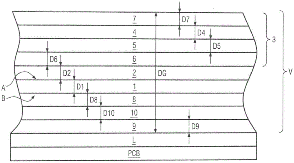
图1示出了根据本发明的复合材料的实施方式的放大的原理剖视图,其中,包含在其中的层厚度纯粹示意性地且未按正确比例示出,1 shows an enlarged schematic sectional view of an embodiment of a composite material according to the invention, wherein the layer thicknesses contained therein are shown purely schematically and not to scale,
图2示出了作为根据本发明的光电装置的示例的发光装置的实施方式的部分区域的俯视图,2 shows a top view of a partial area of an embodiment of a light emitting device as an example of an optoelectronic device according to the invention,
图3示出了用于根据本发明的光电的、尤其是发光的装置的由根据本发明的复合材料构成的框架支承结构的实施方式的俯视图,以及3 shows a top view of an embodiment of a frame support structure made of a composite material according to the invention for an optoelectronic, in particular light-emitting, device according to the invention, and
图4示出了作为根据本发明的光电装置的示例的发光装置的实施方式的横截面。Fig. 4 shows a cross-section of an embodiment of a light emitting device as an example of an optoelectronic device according to the invention.
具体实施方式Detailed ways
对于接下来的描述需要着重强调的是,本发明不限于该实施例并且同时也不限于描述的特征组合中的所有特征或多个特征。而是该实施例的每个单个的部分特征独立于在本文中一起描述的其他所有特征单独地以及与任意的合适的其他特征相结合都具有发明的意义。For the ensuing description it must be emphasized that the invention is not limited to this exemplary embodiment and at the same time not to all or a plurality of features in the described combination of features. Rather, each individual subfeature of the exemplary embodiment has inventive significance independently of all other features described together in this text and in combination with any suitable further features.
在图纸的各个附图中,同一部件也始终设置相同的附图标记,从而其通常也仅分别描述一次。In the individual figures of the drawing, identical components are also always provided with the same reference numerals, so that they are also usually only described once in each case.
首先由图1可见,根据本发明的包括由铝制成的载体1的可反射的复合材料V具有位于载体1上的一侧A上的由氧化铝构成的中间层2和施加在中间层2上的增强反射的光学作用的多层系统3。载体1可具有卷材(Coil)的构造,其宽度可达1600mm、优选1250mm且厚度D1约为0.1至1.5mm、优选约0.2至0.8mm。因为位于载体上的所有薄层、尤其是中间层2以及光学作用的多层系统3的层相对小,可忽略,所以载体厚度D1的尺寸同时也代表根据本发明的复合材料V的总厚度DG。First of all, it can be seen from FIG. 1 that the reflective composite material V according to the invention comprising a carrier 1 made of aluminum has an intermediate layer 2 of aluminum oxide on one side A of the carrier 1 and an intermediate layer 2 applied to the intermediate layer 2. Multilayer system 3 for enhanced reflection optics. The carrier 1 may have the configuration of a coil with a width of up to 1600 mm, preferably 1250 mm, and a thickness D 1 of about 0.1 to 1.5 mm, preferably about 0.2 to 0.8 mm. Since all the thin layers located on the carrier, especially the interlayer 2 and the layers of the optically active multilayer system 3 are relatively small and negligible, the dimension of the carrier thickness D1 simultaneously also represents the total thickness of the composite material V according to the invention DG.
载体1的铝尤其可具有高于99.0%的纯度,由此促进其导热性能。由此可防止形成热峰。但是例如载体1也可为带状的铝板Al98.3,即纯度为98.3%。也可使用铝合金、例如AlMg合金作为载体1,只要由其通过阳极氧化可形成中间层2。In particular, the aluminum of the carrier 1 can have a purity of more than 99.0%, thereby promoting its thermal conductivity. This prevents the formation of thermal peaks. However, the carrier 1 can also be, for example, a strip-shaped aluminum plate of Al98.3, ie with a purity of 98.3%. An aluminum alloy, such as an AlMg alloy, can also be used as the carrier 1 as long as the intermediate layer 2 can be formed therefrom by anodic oxidation.
光学作用的多层系统3例如如示出地可由至少三个层构成,其中的两个上层4、5是介电层和/或氧化层,位于其下面的最下层6是金属的、例如由铝或银构成的层,其形成反射层6。The optically active multilayer system 3 can for example consist of at least three layers as shown, the two
此外,在示出的情况下示出了可选存在的、用于保护的非金属的、由吸收率低的材料,例如二氧化硅构成的覆盖层7。这种层结构由德国实用新型DE 2 98 12 559 U1得知,其完全包括在本文中。由此光学的多层系统3的介电层和/或氧化层4、5例如可分别具有在30nm至200nm范围中的厚度D4、D5,其中厚度D4、D5分别优选地为待反射的电磁辐射的光谱范围的平均波长的四分之一,从而层4、5可用作提高反射的干涉层。保护层7的厚度D7可在0.5nm至20nm的范围中、优选在0.5nm至10nm的范围中。也可设置成,在光学的多层系统3上施加氮化硅保护层作为覆盖层7。Furthermore, in the illustrated case, an optionally present protective non-metallic cover layer 7 of a low-absorption material, for example silicon dioxide, is shown. Such a layer structure is known from German Utility Model DE 2 98 12 559 U1, which is fully included here. The dielectric and/or
光学的多层系统3和覆盖层7以及有利地下面还将描述的、尤其构造成铜层的金属或金属合金的层9可以技术有利的方式在使用连续的真空带涂布工艺的情况下进行施加。尤其在此层4、5、6、7、9可为溅射层、尤其是通过反应性溅射产生的层,CVD或PECVD层或通过蒸发、尤其通过电子轰击或由热源产生的层。The optical multilayer system 3 and the cover layer 7 and advantageously the layer 9 of a metal or metal alloy, which will be described further below, in particular in the form of a copper layer, can be produced in a technically advantageous manner using a continuous vacuum belt coating process. apply. In particular, the
反射层6能可选地经由未示出的、例如由氧化铝、氧化钛和/或氧化铬构成的粘附剂层连接到中间层2上。此外,反射层6能可选地在上侧和下侧置入到未示出的例如由镍、镍合金或钯构成的阻挡层之间,以便提高温度稳定性。The reflective layer 6 can optionally be connected to the intermediate layer 2 via an adhesive layer (not shown), for example composed of aluminum oxide, titanium oxide and/or chromium oxide. Furthermore, the reflective layer 6 can optionally be inserted on the top and bottom between barrier layers (not shown), for example of nickel, nickel alloys or palladium, in order to increase the temperature stability.
光学的多层系统3的上部的介电层和/或氧化层4是比光学的多层系统3的下部的介电层和/或氧化层5具有更高的折射率的层,其中,上部的层4优选可由TiO2、Ta2O5、Nb2O5、MoO3和/或ZrO2构成且下部的层5优选可由Al2O3和/或SiO2构成。The upper dielectric layer and/or
根据本发明设置成,由氧化铝构成的、尤其由阳极氧化的铝形成的中间层2具有的厚度D2在5nm至200nm的范围中、优选在10至100nm的范围中。如已经实施地,由此如在图2中所示,有利地根据本发明在所谓的线接合中一方面可将导线D焊接、尤其将金线超声波焊接在根据本发明的复合材料V的前侧或上侧A,从而在复合材料V的表面A和在复合材料V上通过表面安装施加的电子构件SMD之间可以毫无问题地进行电连接(焊接点SP)。According to the invention it is provided that the intermediate layer 2 of aluminum oxide, in particular of anodized aluminum, has a thickness D 2 in the range of 5 nm to 200 nm, preferably in the range of 10 to 100 nm. As already implemented, thus, as shown in FIG. 2 , advantageously according to the invention in so-called wire bonding, on the one hand, a wire D, in particular a gold wire, can be welded in front of the composite material V according to the invention. Side or upper side A, so that an electrical connection (soldering point SP) can be made without problems between the surface A of the composite material V and the electronic components SMD applied by surface mounting on the composite material V.
在此优选地,中间层2的表面具有的算数平均粗糙度Ra在小于0.05μm、尤其小于0.01μm、特别优选小于0.005μm的范围中。这在存在前述的高的总光反射率的情况下用于设置根据DIN5036确定的最小的漫射光反射率。如果需要较高的漫射光反射率,可相应地提高粗糙度。Preferably, the surface of the intermediate layer 2 has an arithmetic mean roughness R a in the range of less than 0.05 μm, in particular less than 0.01 μm, particularly preferably less than 0.005 μm. This serves to set a minimum diffuse light reflectance determined according to DIN 5036 in the presence of the aforementioned high total light reflectance. If higher diffuse light reflectance is desired, the roughness can be increased accordingly.
在载体1的与反射增强的光学作用的多层系统3相反的一侧B上可选地布置由氧化铝构成的另一层8,该层例如可以在上侧A阳极氧化的制造情况下同时产生。但是其形成在必要时可通过遮盖侧B来避免。还已知用于必要时除去这种层的方法。如果存在由氧化铝构成的另一层8,其厚度D8应在与中间层2的厚度D2相同的范围中,即,在5nm至200nm的范围中、优选在10至100nm的范围中。On the side B of the carrier 1 opposite the reflection-enhancing optically active multilayer system 3 , a
另一本发明重要的特征在于,在载体1的与反射增强的、光学作用的多层系统3相反的侧B上在表面施加金属或金属合金的层9,其在25℃下具有的比电阻最大为1.2*10-1Ωmm2/m,其中,在表面施加的层9的厚度D9在10nm至5.0μm的范围中。Another important feature of the invention is that, on the side B of the carrier 1 opposite to the reflection-enhancing, optically active multilayer system 3, a layer 9 of a metal or metal alloy is applied on the surface, which has a specific resistance at 25° C. A maximum of 1.2*10 −1 Ωmm 2 /m, wherein the thickness D 9 of the layer 9 applied on the surface is in the range of 10 nm to 5.0 μm.
尤其可为铜层,以在0.1μm至5.0μm的范围中、优选在0.2μm至3.0μm的范围中、特别优选在0.5μm至1.5μm的范围中的厚度D9施加铜层。In particular it may be a copper layer, which is applied with a thickness D 9 in the range of 0.1 μm to 5.0 μm, preferably in the range of 0.2 μm to 3.0 μm, particularly preferably in the range of 0.5 μm to 1.5 μm.
本发明的另一优选的实施方式是,在表面施加的层9是厚度D9在10nm至500nm的范围中、尤其厚度D9在50nm至250nm的范围中的银层。Another preferred embodiment of the invention is that the layer 9 applied on the surface is a silver layer with a thickness D 9 in the range of 10 nm to 500 nm, in particular a thickness D 9 in the range of 50 nm to 250 nm.
在表面施加的金属或金属合金的层9的比电阻在25℃下优选可具有最大值2.7*10-2Ωmm2/m、特别优选最大值1.8*10-2Ωmm2/m。The specific resistance of the layer 9 of metal or metal alloy applied on the surface can preferably have a maximum value of 2.7*10 −2 Ωmm 2 /m at 25° C., particularly preferably a maximum value of 1.8*10 −2 Ωmm 2 /m.
关于在此不同材料所基于的比电阻的值参考下面表1,该表格基于在文献中各个位置所述的值来总结。For the values of the specific resistances on which the different materials are based here reference is made to Table 1 below, which is summarized based on the values stated in various places in the literature.
表1:在25℃下的比电阻ρ的值Table 1: Values of specific resistance ρ at 25°C

分别具有不同组分的十种不同的二元合金(Al/Cu、Al/Mg、Cu/Au、Cu/Ni、Cu/Pd、Cu/Zn、Au/Pd、Au/Ag、Fe/Ni、Ag/Pd)的比电阻ρ的概览例如参见科学文章“Electricalresistivity of ten selected binary alloys Systems”,作者Ho,C.Y.等,J.Phys.Chem.Ref.Data,第12卷,第2期,1983年,第183至322页。在确定根据本发明设置的层9的特定化学组分时可参考这些值。Ten different binary alloys (Al/Cu, Al/Mg, Cu/Au, Cu/Ni, Cu/Pd, Cu/Zn, Au/Pd, Au/Ag, Fe/Ni, For an overview of the specific resistance ρ of Ag/Pd see for example the scientific article "Electrical resistance of ten selected binary alloys Systems" by Ho, C.Y. et al., J.Phys.Chem.Ref.Data, Vol. 12, No. 2, 1983 , pp. 183-322. These values can be referred to when determining the specific chemical composition of the layer 9 provided according to the invention.
但是也可根据ASTM F390-11“Standard Test Method for Sheet Resistance ofThin Metallic Films With a Collinear Four-Probe-Array”直接测量。该标准也包含对此的说明,例如以单位Ω或“Ω平方”得出的表面电阻(“Sheet Resistance”)在考虑到层几何结构、即其长度、宽度和厚度的情况下可被换算成比电阻。But it can also be measured directly according to ASTM F390-11 "Standard Test Method for Sheet Resistance of Thin Metallic Films With a Collinear Four-Probe-Array". The standard also contains instructions for this, e.g. the sheet resistance ("Sheet Resistance") in the unit Ω or "Ω squared" can be converted into specific resistance.
在由铝制成的载体1或由氧化铝制成的可选存在的另一层8和铜层9之间可以优选地设置粘附剂层10,粘附剂层例如由过渡金属、尤其是由钛、铬或镍制成且其厚度D10优选可在5nm至25nm的范围中、特别优选在10nm至20nm的范围中。Between the support 1 made of aluminum or an optionally present
如刚才所提到的,这有利地使得在根据本发明的复合材料V的后侧或下侧B上的接触电阻较小可忽略。由此可将侧B焊接到印刷电路板PCB上或借助类似的、材料配合作用的连接方法来施加。材料配合作用的连接层在图1和图4中分别用附图标记L表示。对于焊接可有利地使用例如含锡的标准电焊料、例如Sn96.5Ag3Cu0.5。As just mentioned, this advantageously results in negligibly low contact resistance on the rear or underside B of the composite material V according to the invention. The side B can thus be soldered to the printed circuit board PCB or applied by means of a similar material-interactive connection method. The connecting layer of the material interaction is indicated by the reference symbol L in each case in FIGS. 1 and 4 . For soldering, standard solders containing tin, for example Sn96.5Ag3Cu0.5, can advantageously be used.
虽然金属或金属合金的表面层9、尤其是铜层相对薄,但是显示出,在根据本发明的复合材料V和焊料之间没有形成相对于层厚D9厚且脆的金属间的相,其可由于热应力而产生焊接部位的机械失效以及因此电失效。由此直至1000h的热时效处理仅形成几百nm厚的金属间的相。也显示出,连接层L的钎焊连接有利地通过了典型的测试,在连接的构件LF、COB之间的牵拉力或剪切力在温度时效处理之后、例如在120℃以及1000h的情况下降低仅少于2倍。Although the surface layer 9 of the metal or metal alloy, in particular the copper layer, is relatively thin, it has been shown that no intermetallic phases which are thick and brittle relative to the layer thickness D 9 are formed between the composite material V according to the invention and the solder, It can produce mechanical and thus electrical failures of the welds due to thermal stress. A thermal aging treatment of up to 1000 h thus forms only intermetallic phases with a thickness of several hundred nm. It has also been shown that the soldered connection of the connection layer L advantageously passes typical tests, the tensile or shear forces between the connected components LF, COB after temperature aging, for example at 120° C. and in the case of 1000 h The drop rate is only less than 2 times.
在表面施加的金属或金属合金的层9上、尤其在铜层上能可选地布置有未示出的钝化层。该钝化层优选由Ag、Ni、Pd和/或Au(Ag/Ni/Pd/Au)构成且具有的通常厚度在10nm至500nm的范围中,优选在50nm至250nm的范围中。这种层由于贵金属表面可被焊料较好地润湿还有助于制成的SMD构件在PCB上的可焊接性。A passivation layer (not shown) can optionally be arranged on the surface-applied metal or metal alloy layer 9 , in particular on the copper layer. The passivation layer preferably consists of Ag, Ni, Pd and/or Au (Ag/Ni/Pd/Au) and has a typical thickness in the range of 10 nm to 500 nm, preferably in the range of 50 nm to 250 nm. This layer also contributes to the solderability of the finished SMD component on the PCB due to the better wetting of the noble metal surface by the solder.
参见图2和图4,根据本发明的发光装置LV包括根据本发明的可反射的复合材料V,可反射的复合材料可形成用于电子结构元件SMD的框架支承结构LF(“引线框架”),例如构造成裸芯片DIE的发光二极管。这种框架支承结构LF在图3中示出。该框架支承结构在俯视图中示出的形式具有H形的形状,其中,其横梁Q在称为指部F的轨道之间不是直角地、而是如示出地通常倾斜地延伸。这种框架支承结构LF可在技术方面有利地例如制造成冲压件或通过激光切割制造。根据需要也可额外地构造成弯曲件,因为复合材料V可没有质量损失地毫无问题地弯曲。2 and 4, a lighting device LV according to the invention comprises a reflective composite material V according to the invention, which can form a frame support structure LF ("lead frame") for electronic structural components SMD , such as a light-emitting diode constructed as a bare chip DIE. Such a frame support structure LF is shown in FIG. 3 . In the form shown in plan view, the frame support structure has the shape of an H, wherein its beams Q run not at right angles between rails called fingers F, but generally obliquely as shown. Such a frame support structure LF can be produced technically advantageously, for example as a stamped part or by laser cutting. Optionally, it can also be configured as a curved part, since the composite material V can be bent without any loss of mass without problems.
在此,首先可将多个框架支承结构LF组合在一个构造成带状电路板的框架装置中,在其中框架支承结构LF经由接片以区域的形式
在根据本发明的发光装置LV中,电子结构元件SMD/DIE在上侧、即在侧A上放置在框架支承结构LF上并且借助至少一个单独的导线D与框架支承结构LF电接触。除了LED-Die(附图标记:DIE)在图2中还在右下部示出了齐纳二极管Z作为其他的表面安装的电子构件SMD。由电子结构元件SMD或在示出的情况下由两个示出的电子结构元件SMD(DIE和Z)以及框架支承结构LF构成的复合体在下侧(侧B)与印刷电路板PCB导电地材料适配地连接。In the lighting device LV according to the invention, the electronic component SMD/DIE is placed on the frame support structure LF on the upper side, ie on the side A, and is electrically contacted with the frame support structure LF by means of at least one separate line D. In addition to the LED-Die (reference symbol: DIE), FIG. 2 also shows a Zener diode Z as a further surface-mounted electronic component SMD at the bottom right in FIG. 2 . The composite of electronic components SMD or, in the illustrated case, two illustrated electronic components SMD (DIE and Z) and frame support structure LF is electrically conductive on the underside (side B) with printed circuit board PCB material Adaptively connected.
与示出的实施例不同,也可在载体1上布置具有其他层的其他反射增强的系统3。对此尤其提及DE 10 2015 114 095 A1的具有反射增强的银层的这种系统,只要其根据本发明来设置即可。而在WO 2017/032809 A1中描述的系统在中间层2中必须有厚度直至5μm的形成有机层的漆,根据本发明这需要避免。表述“由氧化铝构成的中间层2”根据本申请优选仅封闭地理解为“仅由…构成”,但是在本申请中必要时不完全排除在中间层2中存在部分层。但是在该观点下,此时任何情况下整个中间层2的厚度D2都应处于5nm至200nm的范围中。In contrast to the exemplary embodiment shown, other reflection-enhancing systems 3 with other layers can also be arranged on the carrier 1 . Mention is made here in particular of such a system with a reflection-enhancing silver layer from DE 10 2015 114 095 A1, provided that it is provided according to the invention. Whereas the system described in WO 2017/032809 A1 must have an organic layer-forming lacquer with a thickness of up to 5 μm in the intermediate layer 2 , this has to be avoided according to the invention. According to the present application, the expression “intermediate layer 2 consisting of aluminum oxide” is preferably only to be understood in a closed sense as “consisting exclusively of”, although the presence of sublayers in the intermediate layer 2 may not be completely excluded in this application. From this point of view, however, the thickness D 2 of the entire intermediate layer 2 should in any case be in the range of 5 nm to 200 nm.
虽然光学的多层系统3不仅可具有前述层4、5、6,但是根据本发明由此不允许设置成,在其上作为覆盖层7施加有机的或有机硅的漆层、例如基于如在现有技术中也描述的溶胶-凝胶层。Although the optical multilayer system 3 can not only have the
尤其从示出根据本发明的、尤其发光的光电装置LV或其单个零件的图2至图4中可看出,在光电装置LV的表面上局部地在焊接点SP处、即在与导线D连接的部位处,根据本发明将非由铝制成的金属接合层FA施加到框架支承结构LF上。该金属接合层FA优选可由银制成并且在俯视图中具有圆形或者形成多边形、尤其是矩形,其中,金属接合层遮盖的面的直径或等效直径或棱边长度K(参见图2)在10μm至100μm的范围中、尤其在20μm至40μm的范围中。金属接合层FA可具有在0.5μm至5.0μm的范围中、优选在1.0μm至3.0μm的范围中的厚度DF。接合层FA可通过冷气焊接施加,其中,在接合层FA中的氧含量尤其小于0.5重量百分比、优选小于0.1重量百分比。It can be seen in particular from FIGS. 2 to 4 which show an optoelectronic device LV according to the invention, in particular luminescent, or its individual parts, that locally on the surface of the optoelectronic device LV at the soldering point SP, that is to say with the conductor D At the point of connection, according to the invention, a metallic bonding layer FA not made of aluminum is applied to the frame support structure LF. The metal bonding layer FA can preferably be made of silver and has a circular shape in plan view or forms a polygon, in particular a rectangle, wherein the diameter or equivalent diameter or edge length K (see FIG. 2 ) of the area covered by the metal bonding layer is In the range of 10 μm to 100 μm, especially in the range of 20 μm to 40 μm. The metal bonding layer FA may have a thickness DF in the range of 0.5 μm to 5.0 μm, preferably in the range of 1.0 μm to 3.0 μm. The joining layer FA can be applied by cold-air welding, wherein the oxygen content in the joining layer FA is in particular less than 0.5% by weight, preferably less than 0.1% by weight.
导线D可如已经所述地由金属、尤其由金、银、铜、铂或铝或由其合金和这些金属的材料组合构成和/或具有由金、银、铜、铂或铝或者这些金属的合金构成的表面的涂层。导线优选可具有的直径DD在15μm至35μm的范围中且优选在接合层FA的部位处借助超声波焊接与框架支承结构LF材料适配地连接。The wire D can, as already mentioned, consist of a metal, in particular gold, silver, copper, platinum or aluminum or alloys thereof and material combinations of these metals and/or have The coating of the surface composed of the alloy. The wires can preferably have a diameter DD in the range of 15 μm to 35 μm and are preferably materially connected to the frame support structure LF at the region of the bonding layer FA by means of ultrasonic welding.
技术人员可得出在本申请的范围中其他的适宜的实施方式,但是没有离开本发明的范围。因此例如在图4中用透明的物质M、例如用环氧树脂注塑根据本发明的发光装置LV的表面。替代地或额外地也可经由构造成LED芯片DIE的电子构件SMD设置光学透镜系统。A skilled person may find other suitable embodiments within the scope of the present application without departing from the scope of the present invention. For example, in FIG. 4 the surface of the luminous means LV according to the invention is injection-molded with a transparent substance M, for example with epoxy resin. Alternatively or additionally, an optical lens system can also be provided via an electronic component SMD configured as an LED chip DIE.
如已经提及银层尤其作为反射层6的情况下,这包括,这种层可包含的合金元素在0.001质量百分比至5.0质量百分比的范围中,尤其在0.5质量百分比至3.0质量百分比的范围中。这种合金元素例如可为稀土元素,如钕。这些元素可迁移至例如银的晶界和/或积聚在银层的表面,由此这些元素在那里比更贵重的银更先氧化并且在银粒子上形成微观的薄的保护层。该合金元素的效用可通过额外地加入合金钯、铂、金和/或铜来提高。由此也使得抑制扩散且抵消银晶体的尤其在较高的温度下例如可在其工作状态下出现的聚集。由此有利地使得反射层的老化减速,即,延缓随时间推移和/或由温度产生的反射率下降。As already mentioned in the case of a silver layer in particular as reflective layer 6, this includes that such a layer may contain alloying elements in the range of 0.001% by mass to 5.0% by mass, in particular in the range of 0.5% by mass to 3.0% by mass . Such alloying elements may be, for example, rare earth elements such as neodymium. These elements can migrate, for example, to the grain boundaries of the silver and/or accumulate on the surface of the silver layer, whereby they oxidize there earlier than the more noble silver and form a microscopically thin protective layer on the silver particles. The effectiveness of the alloying elements can be increased by additionally alloying palladium, platinum, gold and/or copper. This also prevents the diffusion and counteracts the aggregation of the silver crystals, which can occur, for example, in its operating state, especially at higher temperatures. This advantageously slows down the aging of the reflective layer, ie delays the decrease in reflectivity over time and/or as a result of temperature.
钯也可作为主要合金元素、优选以在合金的0.5质量百分比至3.0质量百分比的范围中的质量比例加入到银中,其中,可以额外地以较少的或最多相等的比例存在元素铝,金,铂,铜,钽,铬,钛,镍,钴或硅中的一种作为第三合金成分。Palladium can also be added to silver as main alloying element, preferably in a mass proportion in the range of 0.5 mass % to 3.0 mass % of the alloy, wherein the elements aluminum, gold can additionally be present in lesser or at most equal proportions , platinum, copper, tantalum, chromium, titanium, nickel, cobalt or silicon as a third alloy component.
也可以提供铟,钛和/或锡作为银的合金元素。在这方面,例如合适的是合金优选地包含0.5质量百分比至3.0质量百分比的铟和/或锡和/或锑和/或铋,其中,其余为银。Indium, titanium and/or tin can also be provided as alloying elements for silver. In this respect, for example, it is suitable that the alloy preferably contains 0.5% by mass to 3.0% by mass of indium and/or tin and/or antimony and/or bismuth, the remainder being silver.
EP 3 196 334 A1中也描述了在溅射工艺中产生银合金层的合适靶材。Suitable targets for producing silver alloy layers in the sputtering process are also described in EP 3 196 334 A1.
本发明不限于在本文中限定的特征组合,而是也可通过对总共所有公开的单个特征中的特定特征的每个任意的其他组合来限定。这是指,原则上实际上本文的主要技术方案的任一单个特征都可取消或通过本申请在其他位置公开的至少一个单个特征来替代。就此而言本文的主要技术方案仅理解为本发明的第一表述尝试。The invention is not restricted to the combination of features defined here, but can also be defined by any other combination of specific features in all of the individual features disclosed. This means that, in principle, virtually any single feature of the main technical solution herein can be eliminated or replaced by at least one single feature disclosed elsewhere in this application. In this regard, the main technical solution herein is only to be understood as a first attempt to express the present invention.
附图标记列表List of reference signs
1 V的载体1 V carrier
2 V在1上的中间层(侧A)2 V on the middle layer (side A) on 1
3 V在2上的光学作用的多层系统Multilayer system with optical action of 3 V on 2
4、5 3的上部的层(侧A)4, 5 The upper layer of 3 (side A)
6 3的最下层、反射层(侧A)6 The lowest layer of 3, reflective layer (side A)
7 V在3上方的覆盖层(侧A)7 V Overlay on top of 3 (Side A)
8 V在1上的Al2O3层(侧B)8 V Al2O3 layer on 1 ( side B)
9 金属或金属合金的层(侧B)9 Layers of metal or metal alloy (side B)
A 1的上侧The upper side of A 1
B 1的下侧Underside of B 1
D 导线D wire
D1 1的厚度D 1 1 Thickness
D2 2的厚度D 2 2 Thickness
D3 3的厚度D 3 3 Thickness
D4 4的厚度
D5 5的厚度D 5 5 Thickness
D6 6的厚度D 6 6 Thickness
D7 7的厚度D 7 7 Thickness
D8 8的厚度
D9 9的厚度D 9 9 Thickness
DG V的总厚度Total thickness of DG V
DIE 发光二极管、SMD的裸芯片实施方式(图2、4)DIE Light-emitting diodes, bare chip implementation of SMD (Figure 2, 4)
F LF的H形指部(图2、3)H-shaped fingers of F LF (Fig. 2, 3)
FA 接合层FA bonding layer
K FA的棱边长度(图2)Edge length of K FA (Fig. 2)
L 在V和PCB之间的连接层L is the connecting layer between V and PCB
LF 框架支承结构(引线框架)LF frame support structure (lead frame)
LV 具有V的发光的光电装置LV Light-emitting optoelectronic device with V
M LV的透明物质(图4)Transparent substance of M LV (Fig. 4)
PCB 印刷电路板PCB printed circuit board
Q LF的H形横梁(图3)H-shaped beam for Q LF (Fig. 3)
SMD 电子结构元件(表面安装设备)SMD Electronic Structural Components (Surface Mount Devices)
SP 焊接点,在D和LF之间的连接部位(图2、4)SP welding point, at the junction between D and LF (Fig. 2, 4)
V 复合材料V Composite
Z 齐纳二极管、SMD的实施方式(图2)Z Zener diode, SMD implementation (Fig. 2)
Claims (34)
Applications Claiming Priority (5)
| Application Number | Priority Date | Filing Date | Title |
|---|---|---|---|
| DE102017115798.0 | 2017-07-13 | ||
| DE102017115798.0A DE102017115798A1 (en) | 2017-07-13 | 2017-07-13 | Reflective composite material, in particular for surface-mounted components (SMD), and light-emitting device with such a composite material |
| EP17196142.8 | 2017-10-12 | ||
| EP17196142.8A EP3428696B9 (en) | 2017-07-13 | 2017-10-12 | Reflective composite material, in particular for surface-mounted components (smd), and light-emitting device comprising such a composite material |
| PCT/EP2017/081991 WO2019011456A1 (en) | 2017-07-13 | 2017-12-08 | OPTOELECTRONIC DEVICE WITH SURFACE MOUNTED COMPONENT ON A FRAME STRUCTURE AND REFLECTIVE COMPOSITE MATERIAL FOR SUCH A DEVICE |
Publications (2)
| Publication Number | Publication Date |
|---|---|
| CN110870085A CN110870085A (en) | 2020-03-06 |
| CN110870085B true CN110870085B (en) | 2023-05-12 |
Family
ID=60083810
Family Applications (3)
| Application Number | Title | Priority Date | Filing Date |
|---|---|---|---|
| CN201780093051.5A Active CN110870085B (en) | 2017-07-13 | 2017-12-08 | Optoelectronic device with structural elements surface mounted on a frame support structure and reflective composite material for such a device |
| CN201880035201.1A Pending CN110678784A (en) | 2017-07-13 | 2018-06-12 | Reflective composite material, in particular for surface-mounted components (SMD), and light-emitting device comprising such a composite material |
| CN202211267979.XA Pending CN115524773A (en) | 2017-07-13 | 2018-06-12 | Reflective composite material, in particular for surface-mounted components (SMD), and light-emitting device comprising such a composite material |
Family Applications After (2)
| Application Number | Title | Priority Date | Filing Date |
|---|---|---|---|
| CN201880035201.1A Pending CN110678784A (en) | 2017-07-13 | 2018-06-12 | Reflective composite material, in particular for surface-mounted components (SMD), and light-emitting device comprising such a composite material |
| CN202211267979.XA Pending CN115524773A (en) | 2017-07-13 | 2018-06-12 | Reflective composite material, in particular for surface-mounted components (SMD), and light-emitting device comprising such a composite material |
Country Status (12)
| Country | Link |
|---|---|
| US (2) | US11444226B2 (en) |
| EP (2) | EP3428696B9 (en) |
| JP (1) | JP7137868B2 (en) |
| KR (1) | KR102592772B1 (en) |
| CN (3) | CN110870085B (en) |
| DE (2) | DE102017115798A1 (en) |
| ES (1) | ES2928618T3 (en) |
| MY (1) | MY201326A (en) |
| PH (1) | PH12020500088A1 (en) |
| PL (1) | PL3428696T3 (en) |
| TW (2) | TWI661153B (en) |
| WO (2) | WO2019011456A1 (en) |
Cited By (1)
| Publication number | Priority date | Publication date | Assignee | Title |
|---|---|---|---|---|
| CN115524773A (en) * | 2017-07-13 | 2022-12-27 | 阿兰诺德股份有限两合公司 | Reflective composite material, in particular for surface-mounted components (SMD), and light-emitting device comprising such a composite material |
Families Citing this family (4)
| Publication number | Priority date | Publication date | Assignee | Title |
|---|---|---|---|---|
| DE102018107667B4 (en) | 2018-03-15 | 2026-01-29 | OSRAM Opto Semiconductors Gesellschaft mit beschränkter Haftung | OPTOELECTRONIC SEMICONDUCTOR CHIP |
| JP7177001B2 (en) * | 2019-05-23 | 2022-11-22 | 日本化薬株式会社 | Dibenzopyromethene boron chelate compound, near-infrared light absorbing dye, photoelectric conversion device, near-infrared light sensor and imaging device |
| DE102019118793A1 (en) * | 2019-07-11 | 2021-01-14 | OSRAM Opto Semiconductors Gesellschaft mit beschränkter Haftung | OPTOELECTRONIC COMPONENT |
| KR102907867B1 (en) * | 2020-09-24 | 2026-01-02 | 삼성전자 주식회사 | image sensor package |
Citations (6)
| Publication number | Priority date | Publication date | Assignee | Title |
|---|---|---|---|---|
| CN1370854A (en) * | 2000-12-20 | 2002-09-25 | 阿兰诺德精炼铝厂股份有限两合公司 | Composite material |
| EP1876653A2 (en) * | 2006-07-07 | 2008-01-09 | LG Electronics Inc. | Sub-mount for mounting light emitting device and light emitting device package |
| CN103101249A (en) * | 2011-11-10 | 2013-05-15 | 阿兰诺德股份有限两合公司 | Laser welding composite material for solar collector |
| CN204946920U (en) * | 2014-04-23 | 2016-01-06 | 西铁城电子株式会社 | LED luminaire |
| DE102015211843A1 (en) * | 2015-06-25 | 2016-12-29 | Conti Temic Microelectronic Gmbh | Electronic component and method for producing an electronic component |
| DE102015114095A1 (en) * | 2015-08-25 | 2017-03-02 | Alanod Gmbh & Co. Kg | Reflecting composite material with an aluminum support and with a silver reflection layer |
Family Cites Families (52)
| Publication number | Priority date | Publication date | Assignee | Title |
|---|---|---|---|---|
| EP1022787B2 (en) | 1989-05-31 | 2012-07-11 | OSRAM Opto Semiconductors GmbH | Method of producing a surface-mountable optical element and surface-mountable optical element |
| JPH08292308A (en) * | 1995-04-24 | 1996-11-05 | Toshiba Lighting & Technol Corp | Reflector and reflective illuminator using the same |
| DE29812559U1 (en) | 1998-07-15 | 1999-11-25 | Alanod Aluminium Veredlung Gmb | Composite material for reflectors |
| ES2205565T3 (en) | 1998-11-12 | 2004-05-01 | ALCAN TECHNOLOGY & MANAGEMENT AG | REFLECTOR WITH RESISTANT SURFACE. |
| SE0000751D0 (en) | 2000-03-07 | 2000-03-07 | Swetree Genomics Ab | Transgenic trees and methods for their production |
| US6407411B1 (en) | 2000-04-13 | 2002-06-18 | General Electric Company | Led lead frame assembly |
| DE10126100A1 (en) | 2001-05-29 | 2002-12-05 | Linde Ag | Production of a coating or a molded part comprises injecting powdered particles in a gas stream only in the divergent section of a Laval nozzle, and applying the particles at a specified speed |
| DE10148567A1 (en) | 2001-10-01 | 2003-07-31 | Basf Ag | Method and device for examining the hardening of curable formulations |
| JP4360788B2 (en) | 2002-08-29 | 2009-11-11 | シチズン電子株式会社 | Backlight for liquid crystal display panel and method of manufacturing light emitting diode used therefor |
| JP5262136B2 (en) | 2008-01-28 | 2013-08-14 | 株式会社村田製作所 | Manufacturing method of electronic parts |
| US20110095310A1 (en) | 2008-03-26 | 2011-04-28 | Shimane Prefectural Government | Semiconductor light emitting module and method of manufacturing the same |
| DE102008029743A1 (en) | 2008-06-25 | 2009-12-31 | Manfred Grimm | Method for producing a downlight reflector |
| CN102265417B (en) * | 2008-12-26 | 2013-10-23 | 古河电气工业株式会社 | Lead frame for optical semiconductor device, manufacturing method thereof, and optical semiconductor device |
| KR101077264B1 (en) * | 2009-02-17 | 2011-10-27 | (주)포인트엔지니어링 | Substrate for optical device, optical device package having the same and menufacturing method thereof |
| CN102369607A (en) * | 2009-03-31 | 2012-03-07 | 东芝照明技术株式会社 | Light emitting device and lighting device |
| WO2011122665A1 (en) | 2010-03-30 | 2011-10-06 | 大日本印刷株式会社 | Leadframe or substrate for led, semiconductor device, and method for manufacturing leadframe or substrate for led |
| DE202010017507U1 (en) * | 2010-04-01 | 2012-01-18 | Alanod Aluminium-Veredlung Gmbh & Co. Kg | Reflector with high resistance to weathering and corrosion |
| US8933548B2 (en) * | 2010-11-02 | 2015-01-13 | Dai Nippon Printing Co., Ltd. | Lead frame for mounting LED elements, lead frame with resin, method for manufacturing semiconductor devices, and lead frame for mounting semiconductor elements |
| CN103180980B (en) * | 2010-11-12 | 2017-04-26 | 三菱综合材料株式会社 | Light-emitting element using composition for reflective film and method for producing same |
| JP5011445B1 (en) * | 2011-06-22 | 2012-08-29 | パナソニック株式会社 | Mounting board and light emitting module |
| DE202011050976U1 (en) * | 2011-08-12 | 2012-11-15 | Alanod Aluminium-Veredlung Gmbh & Co. Kg | Highly reflective substrate for light-emitting diodes and light-emitting device with such a carrier material |
| JP5935577B2 (en) * | 2011-08-23 | 2016-06-15 | 大日本印刷株式会社 | Lead frame for optical semiconductor device, lead frame for optical semiconductor device with resin, and optical semiconductor device |
| US9102851B2 (en) | 2011-09-15 | 2015-08-11 | Trillion Science, Inc. | Microcavity carrier belt and method of manufacture |
| US8739391B2 (en) * | 2011-09-21 | 2014-06-03 | HGST Netherlands B.V. | Silver alloy electrical lapping guides (ELGs) for fabrication of disk drive sliders with magnetoresistive sensors |
| JP5938912B2 (en) | 2012-01-13 | 2016-06-22 | 日亜化学工業株式会社 | Light emitting device and lighting device |
| US9685594B2 (en) | 2012-05-31 | 2017-06-20 | Panasonic Intellectual Property Management Co., Ltd. | LED module and method of preparing the LED module, lighting device |
| KR101886157B1 (en) * | 2012-08-23 | 2018-08-08 | 엘지이노텍 주식회사 | Light emitting deviceand lighting system |
| DE102012108719A1 (en) * | 2012-09-17 | 2014-03-20 | Alanod Gmbh & Co. Kg | Reflector for lighting fixture e.g. lamp, has transparent layer that is provided with metallic support layer in regions provided with electrical connection to light source, and electrical circuit is used as connection structure |
| TW201427113A (en) * | 2012-12-21 | 2014-07-01 | 財團法人工業技術研究院 | Solid crystal method and solid crystal structure of light emitting diode package |
| US10295124B2 (en) * | 2013-02-27 | 2019-05-21 | Cree, Inc. | Light emitter packages and methods |
| JP6291713B2 (en) * | 2013-03-14 | 2018-03-14 | 日亜化学工業株式会社 | Light-emitting element mounting substrate, light-emitting device including the same, and lead frame |
| JP6032086B2 (en) * | 2013-03-25 | 2016-11-24 | 豊田合成株式会社 | Light emitting device |
| CN203277501U (en) * | 2013-05-14 | 2013-11-06 | 李刚 | Substrate structure with light reflection layer and semiconductor luminescent source |
| US9865783B2 (en) * | 2013-09-09 | 2018-01-09 | Luminus, Inc. | Distributed Bragg reflector on an aluminum package for an LED |
| DE102013218541A1 (en) * | 2013-09-16 | 2015-03-19 | Osram Gmbh | Light module with semiconductor light sources and carrier plate |
| WO2015092781A1 (en) | 2013-12-19 | 2015-06-25 | Koninklijke Philips N.V. | Light emitting device package |
| JP2015126137A (en) * | 2013-12-26 | 2015-07-06 | アピックヤマダ株式会社 | Lead frame, LED package substrate, reflector member, LED package, light emitting device, light emitting system, and LED package substrate and LED package manufacturing method |
| JP2015169677A (en) | 2014-03-04 | 2015-09-28 | コニカミノルタ株式会社 | Manufacturing method of polarizing laminated film and manufacturing method of polarizing plate |
| JP2015201608A (en) * | 2014-04-10 | 2015-11-12 | 大日本印刷株式会社 | Lead frame with resin and manufacturing method of lead frame with resin and led package and manufacturing method of led package |
| US20150349221A1 (en) * | 2014-05-30 | 2015-12-03 | Bridgelux, Inc. | Light-emitting device package |
| JP5975186B1 (en) | 2015-02-27 | 2016-08-23 | 三菱マテリアル株式会社 | Ag alloy sputtering target and method for producing Ag alloy film |
| US10559731B1 (en) * | 2015-03-04 | 2020-02-11 | Bridgelux Inc. | Highly reliable and reflective LED substrate |
| US10639702B2 (en) | 2015-03-06 | 2020-05-05 | Eisenbau Kramer Gmbh | Method and coating device for applying a cladding layer during the production of a multilayer heavy-duty pipe |
| DE102015004633B4 (en) | 2015-04-10 | 2017-07-13 | Ellenberger & Poensgen Gmbh | Power distribution system for connection to an AC voltage network |
| DE102015105596A1 (en) | 2015-04-13 | 2016-10-13 | Jürgen Buchstaller | Device for holding a bait |
| DE202015009414U1 (en) | 2015-06-05 | 2017-07-05 | Johann Borgers GmbH | Automotive interior paneling material and automotive interior panel component |
| DE102015114094A1 (en) | 2015-08-25 | 2017-03-02 | Alanod Gmbh & Co. Kg | Reflective composite material with painted aluminum support and with a silver reflection layer and method for its production |
| DE202015008045U1 (en) | 2015-10-09 | 2015-12-09 | Clariant International Ltd. | Universal pigment dispersions based on N-alkylglucamines |
| KR102486032B1 (en) * | 2015-11-04 | 2023-01-11 | 쑤저우 레킨 세미컨덕터 컴퍼니 리미티드 | Light emitting device and lighting apparatus having thereof |
| CN106328641B (en) * | 2016-10-11 | 2018-12-28 | 华南师范大学 | Visible light communication LED with spiral inductance and preparation method thereof |
| WO2018180724A1 (en) * | 2017-03-28 | 2018-10-04 | 東芝マテリアル株式会社 | Semiconductor light emitting element |
| DE102017115798A1 (en) * | 2017-07-13 | 2019-01-17 | Alanod Gmbh & Co. Kg | Reflective composite material, in particular for surface-mounted components (SMD), and light-emitting device with such a composite material |
-
2017
- 2017-07-13 DE DE102017115798.0A patent/DE102017115798A1/en not_active Withdrawn
- 2017-10-12 ES ES17196142T patent/ES2928618T3/en active Active
- 2017-10-12 EP EP17196142.8A patent/EP3428696B9/en active Active
- 2017-10-12 PL PL17196142.8T patent/PL3428696T3/en unknown
- 2017-11-17 TW TW106139933A patent/TWI661153B/en active
- 2017-12-08 DE DE112017007738.9T patent/DE112017007738A5/en not_active Withdrawn
- 2017-12-08 CN CN201780093051.5A patent/CN110870085B/en active Active
- 2017-12-08 WO PCT/EP2017/081991 patent/WO2019011456A1/en not_active Ceased
- 2017-12-08 US US16/629,846 patent/US11444226B2/en active Active
-
2018
- 2018-06-12 CN CN201880035201.1A patent/CN110678784A/en active Pending
- 2018-06-12 MY MYPI2020000115A patent/MY201326A/en unknown
- 2018-06-12 JP JP2020501555A patent/JP7137868B2/en active Active
- 2018-06-12 CN CN202211267979.XA patent/CN115524773A/en active Pending
- 2018-06-12 KR KR1020197036842A patent/KR102592772B1/en active Active
- 2018-06-12 EP EP18729162.0A patent/EP3652569B1/en active Active
- 2018-06-12 WO PCT/EP2018/065516 patent/WO2019011554A1/en not_active Ceased
- 2018-06-12 US US16/629,814 patent/US11469357B2/en active Active
- 2018-06-15 TW TW107120783A patent/TW201909457A/en unknown
-
2020
- 2020-01-10 PH PH12020500088A patent/PH12020500088A1/en unknown
Patent Citations (7)
| Publication number | Priority date | Publication date | Assignee | Title |
|---|---|---|---|---|
| CN1370854A (en) * | 2000-12-20 | 2002-09-25 | 阿兰诺德精炼铝厂股份有限两合公司 | Composite material |
| EP1876653A2 (en) * | 2006-07-07 | 2008-01-09 | LG Electronics Inc. | Sub-mount for mounting light emitting device and light emitting device package |
| KR20080004931A (en) * | 2006-07-07 | 2008-01-10 | 엘지이노텍 주식회사 | Light emitting device package and its manufacturing method |
| CN103101249A (en) * | 2011-11-10 | 2013-05-15 | 阿兰诺德股份有限两合公司 | Laser welding composite material for solar collector |
| CN204946920U (en) * | 2014-04-23 | 2016-01-06 | 西铁城电子株式会社 | LED luminaire |
| DE102015211843A1 (en) * | 2015-06-25 | 2016-12-29 | Conti Temic Microelectronic Gmbh | Electronic component and method for producing an electronic component |
| DE102015114095A1 (en) * | 2015-08-25 | 2017-03-02 | Alanod Gmbh & Co. Kg | Reflecting composite material with an aluminum support and with a silver reflection layer |
Cited By (1)
| Publication number | Priority date | Publication date | Assignee | Title |
|---|---|---|---|---|
| CN115524773A (en) * | 2017-07-13 | 2022-12-27 | 阿兰诺德股份有限两合公司 | Reflective composite material, in particular for surface-mounted components (SMD), and light-emitting device comprising such a composite material |
Also Published As
| Publication number | Publication date |
|---|---|
| TW201908645A (en) | 2019-03-01 |
| TW201909457A (en) | 2019-03-01 |
| US11444226B2 (en) | 2022-09-13 |
| EP3428696A1 (en) | 2019-01-16 |
| EP3428696B1 (en) | 2022-07-20 |
| CN110678784A (en) | 2020-01-10 |
| JP7137868B2 (en) | 2022-09-15 |
| EP3652569C0 (en) | 2024-08-14 |
| TWI661153B (en) | 2019-06-01 |
| DE112017007738A5 (en) | 2020-04-09 |
| US20210367111A1 (en) | 2021-11-25 |
| WO2019011554A1 (en) | 2019-01-17 |
| PH12020500088A1 (en) | 2020-09-14 |
| WO2019011456A1 (en) | 2019-01-17 |
| KR20200026195A (en) | 2020-03-10 |
| EP3428696B9 (en) | 2022-09-28 |
| ES2928618T3 (en) | 2022-11-21 |
| CN115524773A (en) | 2022-12-27 |
| DE102017115798A1 (en) | 2019-01-17 |
| EP3652569B1 (en) | 2024-08-14 |
| KR102592772B1 (en) | 2023-10-20 |
| JP2020526935A (en) | 2020-08-31 |
| PL3428696T3 (en) | 2022-11-14 |
| US20200194641A1 (en) | 2020-06-18 |
| US11469357B2 (en) | 2022-10-11 |
| MY201326A (en) | 2024-02-16 |
| US20210167262A9 (en) | 2021-06-03 |
| EP3652569A1 (en) | 2020-05-20 |
| CN110870085A (en) | 2020-03-06 |
Similar Documents
| Publication | Publication Date | Title |
|---|---|---|
| CN110870085B (en) | Optoelectronic device with structural elements surface mounted on a frame support structure and reflective composite material for such a device | |
| CN100499099C (en) | Lead frame of semiconductor device | |
| TWI557933B (en) | A manufacturing method of a wire frame or a substrate for a light emitting diode, a semiconductor device, and a wire frame or a substrate for a light emitting diode | |
| TWI514629B (en) | A semiconductor light-emitting element mounting substrate, and a semiconductor light-emitting device using the same | |
| US20110121326A1 (en) | Submount Having Reflective Cu-Ni-Ag Pads Formed Using Electroless Deposition | |
| US20060147746A1 (en) | Ceramic substrate, ceramic package for housing light emitting element | |
| JP5578960B2 (en) | Lead frame for optical semiconductor device and manufacturing method thereof | |
| TW201225222A (en) | Carrier substrate for an optoelectronic component, method for its production and optoelectronic component | |
| JP7348567B2 (en) | Metal material for optical semiconductor devices, method for manufacturing the same, and optical semiconductor devices using the same | |
| JP5089795B2 (en) | Optical semiconductor device lead frame, optical semiconductor device lead frame manufacturing method, and optical semiconductor device | |
| JP3940124B2 (en) | apparatus | |
| JP5771124B2 (en) | LED lead frame and manufacturing method thereof | |
| JP5767577B2 (en) | LED lead frame and manufacturing method thereof | |
| JP2012039109A (en) | Lead frame or substrate for led, semiconductor device, and method for manufacturing lead frame or substrate for led | |
| JP2010206034A (en) | Lead frame for optical semiconductor device, package for the optical semiconductor device, the optical semiconductor device, production method of lead frame for optical semiconductor device, production method of package for the optical semiconductor device, and production method of the optical semiconductor device | |
| CN102403437A (en) | Substrate for carrying semiconductor light-emitting element and semiconductor light-emitting device using the substrate | |
| JP2018022835A (en) | Electronic component member, LED package, and LED module | |
| JP6123215B2 (en) | Light emitting device | |
| JP2009267274A (en) | Wiring board for mounting light emitting device | |
| KR101380387B1 (en) | Light emitting diode package | |
| TWI447933B (en) | Vertical led with eutectic layer | |
| TWI796363B (en) | Light-emitting device | |
| JP2010251405A (en) | Light reflecting material and light emitting diode device using the same |
Legal Events
| Date | Code | Title | Description |
|---|---|---|---|
| PB01 | Publication | ||
| PB01 | Publication | ||
| SE01 | Entry into force of request for substantive examination | ||
| SE01 | Entry into force of request for substantive examination | ||
| GR01 | Patent grant | ||
| GR01 | Patent grant |