CN111009727B - Integrated antenna unit design - Google Patents
Integrated antenna unit design Download PDFInfo
- Publication number
- CN111009727B CN111009727B CN201911290385.9A CN201911290385A CN111009727B CN 111009727 B CN111009727 B CN 111009727B CN 201911290385 A CN201911290385 A CN 201911290385A CN 111009727 B CN111009727 B CN 111009727B
- Authority
- CN
- China
- Prior art keywords
- continuous conductor
- antenna
- antenna unit
- module
- electrically connected
- Prior art date
- Legal status (The legal status is an assumption and is not a legal conclusion. Google has not performed a legal analysis and makes no representation as to the accuracy of the status listed.)
- Active
Links
- 238000013461 design Methods 0.000 title claims abstract description 83
- 239000004020 conductor Substances 0.000 claims abstract description 216
- 230000008878 coupling Effects 0.000 claims description 78
- 238000010168 coupling process Methods 0.000 claims description 78
- 238000005859 coupling reaction Methods 0.000 claims description 78
- 238000001914 filtration Methods 0.000 claims description 77
- 230000003071 parasitic effect Effects 0.000 claims description 74
- 239000003990 capacitor Substances 0.000 claims description 18
- 238000001514 detection method Methods 0.000 claims description 8
- 238000004891 communication Methods 0.000 abstract description 12
- 230000010354 integration Effects 0.000 abstract description 8
- 230000005284 excitation Effects 0.000 abstract description 4
- 238000010586 diagram Methods 0.000 description 20
- 230000005855 radiation Effects 0.000 description 15
- 239000002184 metal Substances 0.000 description 11
- 230000005540 biological transmission Effects 0.000 description 10
- 238000004088 simulation Methods 0.000 description 4
- 230000000717 retained effect Effects 0.000 description 3
- 230000008859 change Effects 0.000 description 2
- 230000006698 induction Effects 0.000 description 2
- 238000009434 installation Methods 0.000 description 2
- 238000000034 method Methods 0.000 description 2
- 230000004048 modification Effects 0.000 description 2
- 238000012986 modification Methods 0.000 description 2
- 230000009467 reduction Effects 0.000 description 2
- 230000001105 regulatory effect Effects 0.000 description 2
- 238000010521 absorption reaction Methods 0.000 description 1
- 238000013459 approach Methods 0.000 description 1
- 230000007547 defect Effects 0.000 description 1
- 230000000694 effects Effects 0.000 description 1
- 239000003571 electronic cigarette Substances 0.000 description 1
- 239000007769 metal material Substances 0.000 description 1
- 230000005404 monopole Effects 0.000 description 1
- 150000003071 polychlorinated biphenyls Chemical class 0.000 description 1
- 239000000523 sample Substances 0.000 description 1
- 238000012360 testing method Methods 0.000 description 1
Images









Classifications
-
- H—ELECTRICITY
- H01—ELECTRIC ELEMENTS
- H01Q—ANTENNAS, i.e. RADIO AERIALS
- H01Q1/00—Details of, or arrangements associated with, antennas
- H01Q1/48—Earthing means; Earth screens; Counterpoises
-
- H—ELECTRICITY
- H01—ELECTRIC ELEMENTS
- H01Q—ANTENNAS, i.e. RADIO AERIALS
- H01Q1/00—Details of, or arrangements associated with, antennas
- H01Q1/50—Structural association of antennas with earthing switches, lead-in devices or lightning protectors
-
- H—ELECTRICITY
- H01—ELECTRIC ELEMENTS
- H01Q—ANTENNAS, i.e. RADIO AERIALS
- H01Q1/00—Details of, or arrangements associated with, antennas
- H01Q1/52—Means for reducing coupling between antennas; Means for reducing coupling between an antenna and another structure
-
- H—ELECTRICITY
- H01—ELECTRIC ELEMENTS
- H01Q—ANTENNAS, i.e. RADIO AERIALS
- H01Q13/00—Waveguide horns or mouths; Slot antennas; Leaky-waveguide antennas; Equivalent structures causing radiation along the transmission path of a guided wave
- H01Q13/10—Resonant slot antennas
-
- H—ELECTRICITY
- H01—ELECTRIC ELEMENTS
- H01Q—ANTENNAS, i.e. RADIO AERIALS
- H01Q23/00—Antennas with active circuits or circuit elements integrated within them or attached to them
Landscapes
- Support Of Aerials (AREA)
- Details Of Aerials (AREA)
Abstract
The present invention provides an integrated antenna unit design comprising: a continuous conductor disposed on at least one side of the electronic functional device; the alternating current feeding module is used for feeding alternating current into the continuous conductor; the antenna is electrically connected with the alternating current feeding module with reference to the ground. By utilizing the inherent spatial position of the electronic function device, the continuous conductor is arranged on at least one side of the electronic function device and is used as a resonance element and/or an excitation source of the antenna unit, the wireless communication performance of the antenna unit is realized, the original performance of the electronic function device is kept unchanged, the electronic function device and the antenna unit are simultaneously designed under the environment without antenna clearance or with clearance as small as possible, the electronic function device and the antenna unit are subjected to spatial multiplexing, and the possibility is provided for further high integration of electronic equipment; in addition, different filter modules are designed, and mutual interference between the electronic functional device and the antenna unit is reduced.
Description
Technical Field
The invention relates to the field of design of antenna structures, in particular to an integrated antenna unit design.
Background
Wireless communication is a communication method for exchanging information using electromagnetic wave signals. The antenna element plays an important role in wireless communication as a carrier for radiating and/or receiving electromagnetic waves. The wireless communication frequency band has undergone the evolution of 2G, 3G and 4G times, and is now advancing to the 5G time. Each evolution brings about a change of the life of people. With the advent of the 5G era, more and more electronic products (wireless earphones, wireless intelligent sound boxes, electronic cigarettes with wireless connection functions and the like) are added to large families in wireless communication. However, the electronic devices are stacked more and more closely, and the integration level is higher and higher, which puts higher and higher demands on the integration level of the communication system at present.
Therefore, the prior art still needs to be improved and developed.
Disclosure of Invention
In view of the above-mentioned shortcomings of the prior art, it is an object of the present invention to provide an integrated antenna unit design for solving the problems of low integration level of the wireless communication system in the prior art.
To achieve the above and other related objects, the present invention provides an integrated antenna unit design, the antenna unit at least comprising:
a continuous conductor disposed on at least one side of the electronic functional device;
the alternating current feeding module is used for feeding alternating current into the continuous conductor;
the antenna is electrically connected with the alternating current feeding module with reference to the ground.
Optionally, the integrated antenna unit design further comprises a first high frequency filtering module;
the AC feeding module includes: a feeder line and an AC power supply;
two ends of the feeder line are respectively electrically connected with the antenna reference ground and the continuous conductor;
the alternating current power supply is loaded on the feeder line;
the first high-frequency filtering module is arranged on a signal wire of the electronic functional device.
Optionally, the electronic function device is disposed in a metal piece windowing region, the continuous conductor is disposed on at least one side of the electronic function device, the metal piece is the antenna reference ground, the ac power supply is loaded on the continuous conductor through the feeder, the first high-frequency filtering module is disposed on a signal line of the electronic function device, and the continuous conductor excites the windowing region to form a slot antenna.
Optionally, the electronic function device is disposed in a metal cavity structure, the continuous conductor is disposed on at least one side of the electronic function device, the metal cavity is the antenna ground reference, the ac power supply is loaded on the continuous conductor through the feeder line, the first high-frequency filtering module is disposed on a signal line of the electronic function device, and the continuous conductor excites the metal cavity to form a cavity radiation antenna.
Optionally, the electronic functional device is electrically connected to the continuous conductor through a second high-frequency filtering module, and the ac power supply is electrically connected to the continuous conductor through a first low-frequency filtering module.
Optionally, the integrated antenna unit design further comprises a first high frequency filtering module;
the AC feeding module includes: the system comprises an alternating current feed source, a coupling feed branch section and a first end face impedance adjusting module;
one end of the alternating current feed source is electrically connected with the antenna reference ground, and the other end of the alternating current feed source is electrically connected with one end of the coupling feed branch section;
the other end of the coupling feed branch section is suspended in the air;
two ends of the first end face impedance adjusting module are respectively and electrically connected with the antenna reference ground and the continuous conductor;
the first high-frequency filtering module is arranged on a signal wire of the electronic functional device;
the coupling feed branch section and the continuous conductor are arranged at intervals, and the projection of the coupling feed branch section and the projection of the continuous conductor are at least partially overlapped.
Optionally, the electronic functional device is electrically connected to the continuous conductor through a second high-frequency filtering module, and the first end-face impedance adjusting module is electrically connected to the continuous conductor through a first low-frequency filtering module.
Optionally, the continuous conductor is disposed on at least one side of the electronic functional device and extends to the bottom of the signal line of the electronic functional device;
the electronic functional device is electrically connected with the continuous conductor through a second high-frequency filtering module;
the AC feeding module includes: the system comprises an alternating current feed source, a coupling feed branch section and a first end face impedance adjusting module; one end of the alternating current feed source is electrically connected with the antenna reference ground, and the other end of the alternating current feed source is electrically connected with one end of the coupling feed branch section; the other end of the coupling feed branch section is suspended in the air; the first end face impedance adjusting module is a short circuit wire between the continuous conductor at the bottom of the signal wire of the electronic functional device and the antenna reference ground, and a second low-frequency filtering module is arranged on the short circuit wire;
the coupling feed branch section and the continuous conductor are arranged at intervals, and the projection of the coupling feed branch section and the projection of the continuous conductor are at least partially overlapped.
Optionally, the integrated antenna unit design further includes a second end impedance adjusting module, and two ends of the second end impedance adjusting module are electrically connected to the antenna reference ground and the continuous conductor, respectively.
Optionally, the continuous conductor is disposed on at least one side of the electronic functional device and extends to the bottom of the signal line of the electronic functional device; the alternating current feeding module comprises a feeder line and an alternating current feeding source loaded on the feeder line; the second end face impedance adjusting module is a short connecting wire between the continuous conductor at the bottom of the signal wire of the electronic functional device and the antenna reference ground.
Optionally, the electronic functional device is electrically connected to the continuous conductor through a second high-frequency filtering module, the ac power supply is electrically connected to the continuous conductor through a first low-frequency filtering module, and the short circuit line is provided with a second low-frequency filtering module.
Optionally, the integrated antenna unit design further includes a first high-frequency filtering module disposed on a signal line of the electronic functional device.
Optionally, the continuous conductor is disposed on at least one side of the electronic functional device and extends to the bottom of the signal line of the electronic functional device;
the AC feeding module includes: the antenna comprises an alternating current feed source, a coupling feed branch section and a first end face impedance adjusting module, wherein one end of the alternating current feed source is electrically connected with the antenna reference ground, and the other end of the alternating current feed source is electrically connected with one end of the coupling feed branch section; the other end of the coupling feed branch section is suspended in the air; two ends of the first end face impedance adjusting module are respectively and electrically connected with the antenna reference ground and the continuous conductor;
the second end face impedance adjusting module is a short connecting wire between the continuous conductor at the bottom of the signal wire of the electronic functional device and the antenna reference ground.
Optionally, the electronic function device is electrically connected to the continuous conductor through a second high-frequency filtering module, the first end-face impedance adjusting module is electrically connected to the continuous conductor through a first low-frequency filtering module, and the short circuit line is provided with a second low-frequency filtering module.
Optionally, the integrated antenna unit design further includes a first high-frequency filtering module, and the first high-frequency filtering module is disposed on a signal line of the electronic functional device;
the AC feeding module includes: the antenna comprises an alternating current feed source, a coupling feed branch section and a first end face impedance adjusting module, wherein one end of the alternating current feed source is electrically connected with the antenna reference ground, and the other end of the alternating current feed source is electrically connected with one end of the coupling feed branch section; the other end of the coupling feed branch section is suspended in the air; and two ends of the first end face impedance adjusting module are respectively and electrically connected with the antenna reference ground and the continuous conductor.
Optionally, the integrated antenna unit design further includes a parasitic stub, one end of the parasitic stub is electrically connected to the antenna reference ground, and the other end of the parasitic stub is suspended.
Further, the electronic functional device is a battery of an in-ear headphone, and the continuous conductor surrounds the entire battery;
the integrated antenna unit design comprises: the antenna comprises a continuous conductor, an alternating current feed module, an antenna reference ground and a parasitic branch section;
the AC feeding module includes: the antenna comprises a feeder line, an alternating current feeder source and a first high-frequency filtering module, wherein the first high-frequency filtering module is an inductor arranged on a positive and negative signal line of the battery, a main board is the reference ground of the antenna, two ends of the feeder line are respectively and electrically connected with the main board and the continuous conductor, and the alternating current feeder source is loaded on the feeder line;
the parasitic branch section is an antenna wire, the antenna wire and the continuous conductor are arranged at intervals, and the projections of the antenna wire and the continuous conductor are at least partially overlapped, so that a radiation field generated by the continuous conductor is coupled with a radiation field generated by the antenna wire, and the required resonance is realized.
Optionally, according to any of the above-mentioned integrated antenna unit designs, the continuous conductor is disposed on at least one side of a group of electronic functional devices formed by at least one of the electronic functional devices.
Optionally, the electronic functional device is a proximity sensor, and the continuous conductor is arranged on one side of the proximity sensor and extends to the bottom of the proximity sensor signal line;
the integrated antenna unit design comprises: the antenna comprises a continuous conductor, an alternating current feed module, an antenna reference ground, a second high-frequency filter module, a second low-frequency filter module, a parasitic branch node and other radiators, wherein the second high-frequency filter module is an inductor, the second low-frequency filter module is a capacitor, and the other radiators are antenna extension wiring;
the AC feeding module includes: the antenna comprises an alternating current feed source, a coupling feed branch section and a first end face impedance adjusting module, wherein one end of the alternating current feed source is electrically connected with the antenna reference ground, and the other end of the alternating current feed source is electrically connected with one end of the coupling feed branch section; the other end of the coupling feed branch section is suspended in the air; the first end face impedance adjusting module is a short circuit wire between the continuous conductor at the bottom of the signal wire of the electronic functional device and the antenna reference ground, and a second low-frequency filtering module is arranged on the short circuit wire; the coupling feed branch section and the continuous conductor are arranged at intervals, and the projection of the coupling feed branch section and the projection of the continuous conductor are at least partially overlapped;
the second high-frequency filtering module is electrically connected with a signal detection needle of the proximity sensor and the continuous conductor respectively;
the parasitic branch section and the coupling feed branch section are arranged at intervals, and the projection of the parasitic branch section and the projection of the coupling feed branch section are at least partially overlapped.
The continuous conductor is electrically connected with the antenna extension trace.
Optionally, the electronic functional device is a proximity sensor, and the continuous conductor is arranged on one side of the proximity sensor and extends to the bottom of the proximity sensor signal line;
the integrated antenna unit design comprises: the antenna comprises a continuous conductor, an alternating current feed module, an antenna reference ground, a second end surface impedance adjusting module, a first low-frequency filtering module, a second high-frequency filtering module, other radiators and a parasitic stub, wherein the first low-frequency filtering module and the second low-frequency filtering module are capacitors, the second high-frequency filtering module is an inductor, and the other radiators are antenna extension wiring;
the AC feeding module includes: the antenna comprises a feeder line and an alternating current feeder source loaded on the feeder line, wherein two ends of the feeder line are respectively and electrically connected with the antenna reference ground and the continuous conductor, and the alternating current feeder source is electrically connected with the continuous conductor through the first low-frequency filtering module;
the second end face impedance adjusting module is a short circuit line between the continuous conductor at the bottom of the proximity sensor signal line and the antenna reference ground, and the second low-frequency filtering module is arranged on the short circuit line;
a signal detection needle of the proximity sensor is electrically connected with the continuous conductor through a second high-frequency filtering module;
the parasitic branch section and the antenna extension line are arranged at intervals, and the projection of the parasitic branch section and the antenna extension line is at least partially overlapped.
The continuous conductor is electrically connected with the antenna extension trace.
As described above, in the integrated antenna unit design of the present invention, by using the inherent spatial position of the electronic functional device, the continuous conductor is disposed on at least one side of the electronic functional device, and the continuous conductor is used as the resonant element and/or the excitation source of the antenna unit, so as to achieve the wireless communication performance of the antenna unit, and simultaneously maintain the original performance of the electronic functional device unchanged, and achieve the design of the electronic functional device and the antenna unit under the environment without antenna clearance or with as little clearance as possible, so that the electronic functional device and the antenna unit achieve spatial multiplexing, and make it possible to further increase the integration level of the electronic device; in addition, different filter modules are designed, and mutual interference between the electronic functional device and the antenna unit is reduced.
Drawings
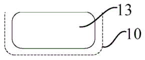
Fig. 1 to fig. 3 are schematic diagrams illustrating the position relationship between the continuous conductor and the electronic functional device in the integrated antenna unit design according to the present invention.
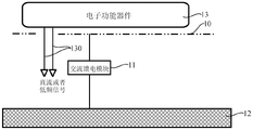
Fig. 4 is a schematic structural diagram of the integrated antenna unit design according to the present invention.
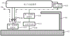
Fig. 5 is a schematic diagram of an integrated antenna unit design with parasitic stubs according to the present invention.
Fig. 6 to 9 are schematic structural diagrams of the integrated antenna unit design according to embodiment 1 of the present invention, in which the current is directly fed.
Fig. 10 to 13 are schematic structural diagrams of the integrated antenna unit design according to embodiment 2 of the present invention, in which the current is a coupling feeding manner.
Fig. 14 to 15 are schematic structural diagrams of the integrated antenna unit design according to embodiment 3 of the present invention, in which the current is a coupling feeding manner.
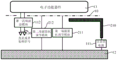
Fig. 16 is a schematic structural diagram of an integrated antenna unit design according to embodiment 4 of the present invention.
Fig. 17 to 20 are schematic structural diagrams of integrated antenna unit designs according to embodiment 5 of the present invention, in which the current is fed directly.
Fig. 21 to 22 are schematic structural diagrams illustrating integrated antenna unit designs according to embodiment 6 of the present invention.
Fig. 23 to 24 are schematic structural diagrams illustrating the integrated antenna unit design according to embodiment 7 of the present invention, in which the current is a coupling feeding manner.
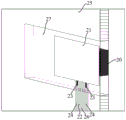
Fig. 25 is a schematic structural diagram of an antenna unit based on a light emitting diode built in a Logo windowing area of a computer screen according to embodiment 8 of the present invention.
Fig. 26 is a schematic longitudinal sectional view taken along a-a in fig. 25.
Fig. 27 is a graph showing simulated return loss of example 8.
FIG. 28 is a graph showing the simulated efficiency of example 8.
Fig. 29 is a schematic structural diagram of an antenna unit based on a horn disposed in a cavity according to embodiment 9 of the present invention.
Fig. 30 shows a simulated return loss plot for example 9.
FIG. 31 is a graph showing the simulated efficiency of example 9.
Fig. 32 is a schematic diagram illustrating an antenna unit structure of a conventional in-ear headphone.
Fig. 33 is a schematic structural diagram of an antenna unit based on a battery of an in-ear earphone according to embodiment 10 of the present invention.
FIG. 34 is a graph showing a comparison of the simulated efficiencies of example 10.
Fig. 35 is a schematic structural diagram of an antenna unit based on a proximity sensor according to embodiment 11 of the present invention.
Fig. 36 is a simplified schematic diagram of fig. 35.
Fig. 37 is a graph showing simulated return loss of example 11.
FIG. 38 is a graph showing the simulated efficiency of example 11.
Fig. 39 is a schematic structural diagram of an antenna unit based on a proximity sensor according to embodiment 12 of the present invention.
Fig. 40 is a simplified schematic diagram of fig. 39.
Fig. 41 is a graph showing simulated return loss of example 12.
FIG. 42 is a graph showing the simulated efficiency of example 12.
Description of the element reference numerals
10. 21, 31, 41, 51, 61 continuous conductor
11 a.c. power supply module
110. 42, 67 feed line
111. 26, 36, 47, 57 and 68 AC power supply
112 first high-frequency filtering module
113 second high frequency filter module
114 first low frequency filtering module
115 second low frequency filter module
210. 58 coupling feed branch section
211. 59 first end face impedance adjusting module
212. 69 second end surface impedance adjusting module
12. 562, 600 antenna reference ground
13 electronic functional device
130. 24, 34, 44 signal line
14. 55, 65 parasitic branch node
15 other radiators
20 light emitting diode
22. 32 FPC transmission line
23. 33, 43, 53, 63 inductance
25 computer screen
27 Logo windowed area
30 loudspeaker unit
35 Metal chamber
40 cell
45 mainboard
46 antenna trace
48 earphone shell
50. 60 proximity sensor
52. 62 signal probe
54. 64 capacitor
56. 66 antenna extension line
561 antenna support
Detailed Description
The embodiments of the present invention are described below with reference to specific embodiments, and other advantages and effects of the present invention will be easily understood by those skilled in the art from the disclosure of the present specification. The invention is capable of other and different embodiments and of being practiced or of being carried out in various ways, and its several details are capable of modification in various respects, all without departing from the spirit and scope of the present invention.
Please refer to fig. 1 to 42. It should be noted that the drawings provided in the present embodiment are only for illustrating the basic idea of the present invention, and the drawings only show the components related to the present invention rather than being drawn according to the number, shape and size of the components in actual implementation, and the type, quantity and proportion of each component in actual implementation may be changed arbitrarily, and the layout of the components may be more complicated. For example, the number of signal lines of the electronic function device is shown as two, but in the actual case, the number of signal lines may be more than two, for example, 5 to 6 in the electronic function device such as a sensor. In addition, for the convenience of understanding, only a part of the signal lines of the electronic functional devices are shown in the drawings, and as a common general knowledge in the field, a person skilled in the art can know that the specific length of the signal lines of the electronic functional devices varies with the position of the signal access terminals on the main board of the whole device structure.
More and more electronic devices begin to introduce wireless communication functions, and along with the higher and higher integration level of the electronic devices, more and more severe tests are provided for the compact spatial layout of the antenna unit; in addition, the electronic device layout design provided by the electronic device manufacturer is not generally changed according to the antenna unit design provided by the antenna unit provider, which also presents a challenge to the compact design of the antenna unit. Based on this, the inventor has analyzed various influencing factors of the prior art and proposed an integrated antenna unit design, as shown in fig. 4, the antenna unit comprises:
a continuous conductor 10 provided on at least one side of the electronic functional device 13;
an ac power feeding module 11 for feeding ac power to the continuous conductor 10;
the antenna is electrically connected to the ac power feeding module 11 with reference to the ground 12.
As shown in fig. 1 to 3, the continuous conductor 10 is provided on at least one side of the electronic functional device 13 as an example. As shown in fig. 1, the continuous conductor 10 may be disposed at the outer periphery of the electronic functional device 13 to enclose the electronic functional device 13 therein; the continuous conductor 10 may be disposed on either side of the electronic functional device 13, as shown in fig. 2, the continuous conductor 10 being disposed on the underside of the electronic functional device 13; as shown in fig. 3, the continuous conductor 10 may be disposed on both sides and the lower side of the electronic functional device 13. The position of the continuous conductor 10 and the electronic functional device 13 may be set in other manners, and may be designed according to the specific situation of the antenna unit, which is not limited herein.
It should be noted that the electronic functional device mentioned in the present invention refers to a device that needs to be powered and can realize some electronic functions (such as light emitting, power generating, sensing, etc.), for example: light emitting diodes, batteries, microphones, USB, Speaker, proximity sensors (P-sensors), etc.
The alternating current feeding module is configured to feed alternating current into the continuous conductor, so that the alternating current can be directly fed by using an alternating current feeding source, or fed by using a radiator in a coupling manner, which is not limited herein. In addition, as known to those skilled in the art, in order to implement the performance of the antenna unit, the ac feeding module may also include an impedance adjusting module (matching or other tuning device) to implement impedance matching of the antenna unit.
The antenna is referred to as a part of an antenna unit, and in an electronic device, the antenna unit may be generally any conductive component such as a main board, a middle frame, a screen, an FPC, a metal-coated bracket, and the like.
The invention utilizes the inherent space position of the electronic function device, realizes the wireless communication function of the antenna unit by arranging the continuous conductor on at least one side of the electronic function device and taking the continuous conductor as the resonance element and/or the excitation source of the antenna unit, simultaneously keeps the original performance of the electronic function device unchanged, realizes the design of the electronic function device and the antenna unit under the environment without antenna clearance or with the smallest clearance as possible, realizes the spatial multiplexing of the electronic function device and the antenna unit, and provides possibility for further high integration of electronic equipment.
As shown in fig. 5, the integrated antenna unit design further includes a parasitic stub 14, and one end of the parasitic stub 14 is electrically connected to the antenna reference ground 12 and the other end is floating. The parasitic branch is added in the antenna unit, and the purpose of widening the bandwidth of the antenna unit can be achieved by coupling and superposing the alternating current feed module with the feed branch and the parasitic branch of the continuous conductor. The opening direction of the parasitic branch and the relative position with the continuous conductor may be set according to the specific requirements of the designed antenna unit, as shown in fig. 5, the parasitic branch is disposed at the lower side of the continuous conductor, and the opening faces the ac power feeding module. In addition, the parasitic stub may be designed simultaneously when the antenna unit of the present invention is designed, or may be provided in the electronic device itself.
As an example, said continuous conductor 10 is arranged on at least one side of a group of electronic functional devices consisting of at least one of said electronic functional devices 13. When the size of the electronic functional device is small, the size of the continuous conductor may not meet the antenna radiation requirement, and at this time, it may be considered that a plurality of electronic functional devices in suitable positions nearby the electronic functional device form an electronic functional device group, and then the continuous conductor is disposed on at least one side of the electronic functional device group to meet the size requirement of the antenna radiation; on the other hand, the combination of a plurality of electronic functional devices as the electronic functional device group can simplify the complex structure among the plurality of electronic functional devices, reduce the mutual influence among the electronic functional devices and improve the performance of the plurality of electronic functional devices.
As an example, the continuous conductor 10 is electrically connected to other radiators. The other radiators can be antenna traces in the forms of PCBs, LDS, FPCs, and the like. Similarly, when the size of the continuous conductor may not meet the antenna radiation requirement, it may be considered to electrically connect other radiators at suitable positions near the continuous conductor to increase the antenna radiation area and meet the antenna unit size requirement.
Here, the above three cases are to be explained, that is: the arrangement of the parasitic stub, the arrangement of the electronic function device group, and the arrangement of the other radiators electrically connected with the continuous conductor may be designed separately or in combination in the antenna unit, specifically, the combination is performed according to the specific requirements of the antenna unit design and the specific design layout of the electronic device, which is not limited herein.
The integrated antenna unit design of the present invention will be described in detail with reference to the specific drawings and the corresponding embodiments, and it should be understood that the described embodiments are only a part of the embodiments of the present invention, and not all embodiments. All other embodiments, which can be derived by a person skilled in the art from the embodiments of the present invention without making any creative effort, shall fall within the protection scope of the present invention.
Example 1
As shown in fig. 6, the present embodiment provides an integrated antenna unit design, which at least includes:
a continuous conductor 10 provided on at least one side of the electronic functional device 13;
the antenna is referenced to ground 12;
a first high frequency filtering module 112;
an ac power feeding module 11 for feeding ac power to the continuous conductor 10, comprising: a feeder line 110 and an ac power supply 111; both ends of the feeder line 110 are electrically connected to the antenna reference ground 12 and the continuous conductor 10, respectively; the ac power supply 111 is loaded on the feeder 110; the first high-frequency filter module 112 is disposed on the signal line 130 of the electronic functional device 13.
The working principle of the antenna unit of the embodiment is as follows: an alternating current power supply 111 feeds alternating current to the continuous conductor 10 by being loaded on the power supply line 110, so that the continuous conductor 10 and the antenna reference ground 12 constitute an antenna radiation unit to radiate electromagnetic waves outwards; in addition, the first high-frequency filtering module 112 cuts off the high-frequency signal to return to the antenna reference ground to form an electric loop with the alternating current power feeding module, which affects the performance of the antenna unit.
As shown in fig. 7, as an example, the integrated antenna unit design may further include a parasitic branch 14, one end of the parasitic branch 14 is electrically connected to the antenna reference ground 12, and the other end is floating, the parasitic branch 14 is spaced apart from the continuous conductor 10, and a projection of the parasitic branch 14 and the continuous conductor 10 at least partially overlap. The opening direction of the parasitic branch 14 and the relative position with respect to the continuous conductor 10 may be set according to the specific requirements of the designed antenna unit, and is not limited herein.
As shown in fig. 8, as an example, the electronic functional device 13 is electrically connected to the continuous conductor 10 through a second high-frequency filtering module 113, and the ac power supply 111 is electrically connected to the continuous conductor 10 through a first low-frequency filtering module 114. The second high-frequency filtering module 113 disconnects the mutual high-frequency signal influence between the antenna unit and the electronic functional device 13, and the first low-frequency filtering module 114 disconnects the low-frequency or direct-current signal between the electronic functional device 13 and the antenna unit, so that the mutual influence between the electronic functional device 13 and the antenna unit is reduced. As shown in fig. 9, preferably, the integrated antenna unit design may further include a parasitic branch 14, one end of the parasitic branch 14 is electrically connected to the antenna reference ground 12, and the other end is floating, the parasitic branch 14 is spaced apart from the continuous conductor 10, and a projection of the parasitic branch 14 and the continuous conductor 10 at least partially overlap. The opening direction of the parasitic branch 14 and the relative position with respect to the continuous conductor 10 may be set according to the specific requirements of the designed antenna unit, and is not limited herein.
It should be noted that, in the following embodiments, the functions of the first high-frequency filtering module 112, the second high-frequency filtering module 113, and the first low-frequency filtering module 114 are the same as those of the present embodiment, so that the functions of the following embodiments will not be described in detail.
Example 2
As shown in fig. 10, the present embodiment provides an integrated antenna unit design, which at least includes:
a continuous conductor 10 provided on at least one side of the electronic functional device 13;
the antenna is referenced to ground 12;
a first high frequency filtering module 112;
an ac power feeding module 11 for feeding ac power to the continuous conductor 10, comprising: the system comprises an alternating current feed source 111, a coupling feed branch section 210 and a first end face impedance adjusting module 211; one end of the ac power supply 111 is electrically connected to the antenna reference ground 12, and the other end is electrically connected to one end of the coupling feed branch 210; the other end of the coupling feed branch section 210 is suspended; both ends of the first end surface impedance adjusting module 211 are electrically connected to the antenna reference ground 12 and the continuous conductor 10, respectively; the first high-frequency filtering module 112 is disposed on the signal line 130 of the electronic functional device 13; the coupling feed branch 210 is spaced apart from the continuous conductor 10, and the coupling feed branch 210 at least partially overlaps the projection of the continuous conductor 10.
The working principle of the antenna unit of the embodiment is as follows: an alternating current power supply 111 is loaded on the coupling feed branch section 210, and the coupling feed branch section 210 and the continuous conductor 10 are mutually coupled to generate effective resonant radiation; in addition, the impedance of the antenna unit is adjusted by matching by the first end surface impedance adjusting module 211. In practical applications, the first end-face impedance adjusting module 211 may be a short circuit, a capacitor, an inductor, or various tuning devices (e.g., a switch, a variable capacitor, etc.).
As shown in fig. 11, as an example, the integrated antenna unit design may further include a parasitic branch 14, one end of the parasitic branch 14 is electrically connected to the antenna reference ground 12, and the other end is floating, the parasitic branch 14 is spaced apart from the coupling feed branch 210, and a projection of the parasitic branch 14 and the coupling feed branch 210 at least partially overlap. The opening direction of the parasitic branch 14 and the relative position with respect to the continuous conductor 10 may be set according to the specific requirements of the designed antenna unit, and is not limited herein.
As shown in fig. 12, the electronic function device 13 is electrically connected to the continuous conductor 10 through a second high-frequency filter module 113, and the first end-face impedance adjusting module 211 is electrically connected to the continuous conductor 10 through a first low-frequency filter module 114, as an example. As shown in fig. 13, preferably, the integrated antenna unit design may further include a parasitic branch 14, one end of the parasitic branch 14 is electrically connected to the antenna reference ground 12, and the other end is floating, the parasitic branch 14 is spaced apart from the continuous conductor 10, and a projection of the parasitic branch 14 and the continuous conductor 10 at least partially overlap.
Example 3
As shown in fig. 14, the present embodiment provides an integrated antenna unit design, which at least includes:
a continuous conductor 10 disposed on at least one side of the electronic functional device 13 and extending to the bottom of the signal line 130 of the electronic functional device 13;
the antenna is referenced to ground 12;
an ac power feeding module 11 for feeding ac power to the continuous conductor 10, comprising: an ac power supply 111, a coupling feed branch 210 and a first end surface impedance adjusting module 211; one end of the ac power supply 111 is electrically connected to the antenna reference ground 12, and the other end is electrically connected to one end of the coupling feed branch 210; the other end of the coupling feed branch section 210 is suspended; the first end face impedance adjusting module 211 is a short-circuit line between the continuous conductor 10 at the bottom of the signal line 130 of the electronic functional device 13 and the antenna reference ground 12, and a second low-frequency filtering module 115 is disposed on the short-circuit line; the coupling feed branch 210 is spaced apart from the continuous conductor 10, and the coupling feed branch 210 at least partially overlaps the projection of the continuous conductor 10;
the electronic functional device 13 is electrically connected to the continuous conductor 10 via a second high-frequency filter module 113.
The working principle of the antenna unit of the embodiment is as follows: an alternating current power supply 111 is loaded on the coupling feed branch section 210 and mutually coupled with the continuous conductor 10 to generate effective resonant radiation; in addition, the impedance of the antenna unit is matched and adjusted by the first end face impedance adjusting module 211, and the low-frequency or direct-current signal between the electronic functional device 13 and the antenna unit is cut off by the first low-frequency filtering module 114, so that the mutual influence between the electronic functional device 13 and the antenna unit is reduced.
As shown in fig. 15, as an example, the integrated antenna unit design may further include a parasitic branch 14, one end of the parasitic branch 14 is electrically connected to the antenna reference ground 12, and the other end is floating, the parasitic branch 14 is spaced apart from the coupling feed branch 210, and a projection of the parasitic branch 14 and the coupling feed branch 210 at least partially overlap.
Example 4
As shown in fig. 16, the present embodiment provides an integrated antenna unit design, which at least includes:
a continuous conductor 10 provided on at least one side of the electronic functional device 13;
an ac power feeding module 11 for feeding ac power to the continuous conductor 10;
an antenna reference ground 12 electrically connected to the ac power feeding module 11;
a second end surface impedance adjusting module 212, and two ends of the second end surface impedance adjusting module 212 are electrically connected to the antenna reference ground 12 and the continuous conductor 10, respectively.
The second end surface impedance adjusting module 212 is configured to perform matching adjustment on the impedance of the antenna unit, and in practical applications, the first end surface impedance adjusting module 211 may be a capacitor, an inductor, or various tuning devices (e.g., a switch, a variable capacitor, etc.).
The ac feeding module 11 is configured to feed ac power to the continuous conductor 10, so the ac power may be fed directly by using an ac power supply, or may be fed by using a radiator in a coupling manner, which is not limited herein. In addition, as known to those skilled in the art, in order to implement the performance of the antenna unit, the ac feeding module may also include an impedance adjusting module (matching or other tuning device) to implement impedance matching of the antenna unit.
Example 5
As shown in fig. 17, the present embodiment provides an integrated antenna unit design, the antenna unit at least includes:
a continuous conductor 10 disposed on at least one side of the electronic functional device 13 and extending to the bottom of the signal line 130 of the electronic functional device 13;
an ac power feeding module 11 for feeding ac power to the continuous conductor 10, comprising: a power supply line 110 and an ac power supply 111 loaded on the power supply line 110;
an antenna reference ground 12 electrically connected to the ac power feed 111;
a second impedance adjusting module 212, wherein the second impedance adjusting module 212 is a short-circuit line between the continuous conductor 10 at the bottom of the signal line 130 of the electronic function device 13 and the antenna reference ground 12.
As shown in fig. 18, as an example, the integrated antenna unit design may further include a parasitic branch 14, one end of the parasitic branch 14 is electrically connected to the antenna reference ground 12, and the other end is floating, the parasitic branch 14 is spaced apart from the continuous conductor 10, and a projection of the parasitic branch 14 and the continuous conductor 10 at least partially overlap. The opening direction of the parasitic branch 14 and the relative position with respect to the continuous conductor 10 may be set according to the specific requirements of the designed antenna unit, and is not limited herein.
As shown in fig. 19, as an example, the electronic functional device 13 is electrically connected to the continuous conductor 10 through a second high-frequency filtering module 113, the ac power supply 111 is electrically connected to the continuous conductor 10 through a first low-frequency filtering module 114, and a second low-frequency filtering module 115 is disposed on the short circuit line. As shown in fig. 20, preferably, the integrated antenna unit design may further include a parasitic branch 14, one end of the parasitic branch 14 is electrically connected to the antenna reference ground 12, and the other end is floating, the parasitic branch 14 is spaced apart from the continuous conductor 10, and a projection of the parasitic branch 14 and the continuous conductor 10 at least partially overlap.
Example 6
As shown in fig. 21, the present embodiment provides an integrated antenna unit design, which at least includes:
a continuous conductor 10 provided on at least one side of the electronic functional device 13;
an ac power feeding module 11 for feeding ac power to the continuous conductor 10;
an antenna reference ground 12 electrically connected to the ac power feeding module 11;
a second end surface impedance adjusting module 212, and two ends of the second end surface impedance adjusting module 212 are electrically connected to the antenna reference ground 12 and the continuous conductor 10, respectively;
and a first high-frequency filtering module 112 disposed on the signal line 130 of the electronic functional device 13.
The second end surface impedance adjusting module 212 is configured to perform matching adjustment on the impedance of the antenna unit, and in practical applications, the first end surface impedance adjusting module 211 may be a capacitor, an inductor, or various tuning devices (e.g., a switch, a variable capacitor, etc.).
The ac feeding module 11 is configured to feed ac power to the continuous conductor 10, so the ac power may be fed directly by using an ac power supply, or may be fed by using a radiator in a coupling manner, which is not limited herein. In addition, as known to those skilled in the art, in order to implement the performance of the antenna unit, the ac feeding module may also include an impedance adjusting module (matching or other tuning device) to implement impedance matching of the antenna unit.
As shown in fig. 22, the ac power feeding module 11 includes, as an example: an ac power supply 111, a coupling feed branch 210 and a first end surface impedance adjusting module 211; one end of the ac power supply 111 is electrically connected to the antenna reference ground 12, and the other end is electrically connected to one end of the coupling feed branch 210; the other end of the coupling feed branch section 210 is suspended; both ends of the first end surface impedance adjusting module 211 are electrically connected to the antenna reference ground 12 and the continuous conductor 10, respectively; the coupling feed branch 210 is spaced apart from the continuous conductor 10, and the coupling feed branch 210 at least partially overlaps the projection of the continuous conductor 10.
As an example, the integrated antenna element design may further include a parasitic stub 14, one end of the parasitic stub 14 is electrically connected to the antenna reference ground 12, and the other end is floating, so as to widen the bandwidth of the antenna element.
Example 7
As shown in fig. 23, the present embodiment provides an integrated antenna unit design, which at least includes:
a continuous conductor 10 disposed on at least one side of the electronic functional device 13 and extending to the bottom of the signal line 130 of the electronic functional device 13;
an antenna reference ground 12 electrically connected to the ac power feed 111;
an ac power feeding module 11 for feeding ac power to the continuous conductor 10, comprising: the antenna comprises an alternating current power supply 111, a coupling feed branch section 210 and a first end face impedance adjusting module 211, wherein one end of the alternating current power supply 111 is electrically connected with the antenna reference ground 12, and the other end of the alternating current power supply is electrically connected with one end of the coupling feed branch section 210; the other end of the coupling feed branch section 210 is suspended; both ends of the first end surface impedance adjusting module 211 are electrically connected to the antenna reference ground 12 and the continuous conductor 10, respectively;
a second impedance adjusting module 212, wherein the second impedance adjusting module 212 is a short-circuit line between the continuous conductor 10 at the bottom of the signal line 130 of the electronic function device 13 and the antenna reference ground 12.
As shown in fig. 24, as an example, the electronic functional device 13 is electrically connected to the continuous conductor 10 through a second high-frequency filtering module 113, the first end-face impedance adjusting module 211 is electrically connected to the continuous conductor 10 through a first low-frequency filtering module 114, and a second low-frequency filtering module 115 is disposed on the short circuit line.
The following embodiments will describe the antenna unit of the present invention in detail with reference to the electronic functional devices in specific electronic equipment, and it is obvious that the electronic functional devices in the specific electronic equipment described are only a part of the embodiments of the present invention, and not all of the embodiments. All embodiments for other electronic functional devices obtained by a person skilled in the art without making creative efforts based on the embodiments of the present invention belong to the protection scope of the present invention.
Example 8
Generally, a certain area of the back cover of the notebook computer screen is a Logo windowing area, the size of the area may be, for example, 38mm × 7mm × 2mm, or may be other sizes, which is mainly determined by the design of the specific computer screen, and a light emitting diode is disposed in the windowing area for lighting the brand Logo. As shown in fig. 25 and 26, in the present embodiment, an antenna unit based on a light emitting diode built in a Logo windowing region of a computer screen is provided based on the light emitting diode, the electronic function device is the light emitting diode 20 built in a Logo windowing region 27 of the computer screen 25, the continuous conductor 21 is disposed at the back of the light emitting diode 20, the power feed line is an fpc (flexible Printed circuit) transmission line 22, the first high-frequency filter module is an inductor 23 disposed on a positive-negative signal line 24 of the light emitting diode 20, the computer screen 25 is the antenna reference ground, and the computer screen is made of a metal material. The ac power supply 26 is applied to the FPC transmission line 22, and the continuous conductor 21 excites the windowed area 27 to form a slot antenna. The thickness of the screen of the notebook computer is limited, so the FPC transmission line is mostly used for supplying power to electronic devices in the screen due to the flat and thin characteristic of the FPC transmission line. The more convenient implementation method can design the continuous conductor and the FPC transmission line into an integrated structure and attach the continuous conductor and the FPC transmission line to the back of the light-emitting diode.
In this embodiment, the structure and the area of the light emitting diode 20 are utilized, so that the function of the wlan (wireless Local area antenna network) antenna unit is realized while the original id (industrial design) design and function of the product are completely retained, and the purpose of spatial multiplexing is achieved. The simulated return loss diagram of the antenna unit in the mounted state of this embodiment is shown in fig. 27, and can cover dual-frequency resonances of 2.4 GHz-2.5 GHz and 5.15 GHz-5.85 GHz. Fig. 28 shows a simulation efficiency chart of the antenna unit in the installation situation of the present embodiment, and the radiation efficiency of the antenna at high and low frequencies can meet the performance index requirement of the WLAN antenna unit.
It should be noted that the continuous conductor of the present embodiment is applied to the light emitting diode in the window area of the computer screen, and can also be applied to other electronic functional devices and window structures with similar structures.
Example 9
As shown in fig. 29, this embodiment provides an antenna unit based on a horn in an electronic device, the electronic function device is the horn unit 30 disposed in a metal cavity 35 (the size of the cavity 35 may be 35mm × 11mm × 10mm, and may also be other sizes, which is mainly determined by the specific design of the electronic device), the continuous conductor 31 is disposed at one side of the horn unit 30, the feeder line is an FPC transmission line 32, the first high-frequency filter module is an inductor 33 disposed on a positive and negative signal lines 34 of the horn 30, the metal cavity 35 is the antenna reference ground, the ac power supply 36 is loaded on the FPC transmission line 32, and the continuous conductor 31 excites the metal cavity 35 to form a cavity radiation antenna. In a preferred embodiment, the continuous conductor 31 structure can be integrated into the same FPC transmission line.
In this embodiment, the structure and the area of the horn unit 30 are utilized, so that the function of the wlan (wireless Local area antenna network) antenna unit is realized while the original id (industrial design) design and function of the product are completely retained, and the purpose of spatial multiplexing is achieved. The simulated return loss diagram of the antenna unit in the mounted state of this embodiment is shown in fig. 30, and can cover dual-frequency resonances of 2.4 GHz-2.5 GHz and 5.15 GHz-5.85 GHz. Fig. 31 shows a simulation efficiency chart of the antenna unit in the installation situation of the present embodiment, and the radiation efficiency of the antenna at high and low frequencies can meet the performance index requirement of the WLAN antenna unit.
It should be noted here that the continuous conductor of the present embodiment is applied to the speaker in the metal cavity, and can also be applied to other electronic functional devices and cavity structures with similar structures.
Example 10
As shown in fig. 32, the size of the antenna unit is 11mm × 11mm × 6.5mm, the antenna trace 46 is attached to the outer side of the earphone housing 48 (generally, a plastic casing), and the ac power supply is connected to the main board 45 and the antenna trace 46 to form a monopole antenna. Due to the size of the headset, the battery 40 occupies a large portion of the overall size of the headset, thereby affecting the antenna unit performance.
As shown in fig. 33, the present embodiment provides a battery-based antenna unit based on the battery 40 of the in-ear headphone, the electronic functional device is the battery 40 of the in-ear headphone, the continuous conductor 41 surrounds the entire battery 40, and the antenna unit includes: a continuous conductor 41, an alternating current feed module, a first high-frequency filter module, an antenna reference ground and a parasitic stub;
the main board 45 is the antenna reference ground, and the first high-frequency filtering module is an inductor 43 disposed on the positive and negative signal lines 44 of the battery 40
The AC feeding module includes: a feeder line 42, an ac power supply 47; wherein, both ends of the feeder line 42 are electrically connected to the motherboard 45 and the continuous conductor 41, respectively, and the ac feeder 47 is loaded on the feeder line 42;
the parasitic stub is an antenna trace 46, the antenna trace 46 and the continuous conductor 41 are arranged at intervals, and projections of the antenna trace 46 and the continuous conductor 41 are at least partially overlapped, so that the continuous conductor 41 and the antenna trace 46 are coupled with each other to realize the required resonance.
In this embodiment, the structure and the area of the battery 40 are utilized, so that the performance of the bt (bluetooth) antenna unit is improved while the original id (industrial design) design and function of the product are completely retained, and the purpose of spatial multiplexing is achieved. Fig. 34 is a comparison graph of simulated efficiency of the antenna unit (upper line in fig. 34) of the in-ear headphone of the present embodiment and the antenna unit (lower line in fig. 34) of the in-ear headphone of the related art, and obviously, the efficiency of the antenna unit of the present embodiment is significantly improved compared to the related art.
It should be noted that the continuous conductor 41 surrounds the entire battery 40 in this embodiment, and the continuous conductor 41 may be disposed on one or more sides of the battery 40 in other embodiments.
Example 11
Radio products are limited by the position of an antenna and the transmitting power of a chip, the performance of the antenna cannot pass the regulatory requirement of SAR (specific Absorption Rate) in many cases, and an SAR reducing sensor is required to be added at the moment, so that the transmitting power of the chip is reduced by sensing the approach of a human body, and the SAR value is ensured to be lower than the regulatory requirement. A commonly used SAR sensor is a P-sensor (proximity sensor). The P-sensor is specifically sized and typically placed outside the antenna clearance area to minimize the impact on antenna performance.
In the embodiment, the spatial multiplexing is carried out on the antenna clearance area (100mm multiplied by 11mm multiplied by 2mm), and the antenna design with the working frequency ranges of 700MHz-960MHz and 1710MHz-2690MHz and the design of the P-sensor are simultaneously realized in the limited space. As shown in fig. 35 and 36, the electronic functional device of the present embodiment is a proximity sensor 50, and the continuous conductor 51 is disposed at one side of the proximity sensor 50 and extends to the bottom of the signal line of the proximity sensor 50;
the antenna unit includes: the antenna comprises a continuous conductor 51, an alternating current feeding module, an antenna reference ground 562, a second high-frequency filtering module, a second low-frequency filtering module, a parasitic branch 55 and other radiators, wherein the second high-frequency filtering module is an inductor 53, the second low-frequency filtering module is a capacitor 54, and the other radiators are antenna extension wiring lines 56;
the AC feeding module includes: an ac power supply 57, a coupling feed branch 58 and a first end-face impedance adjusting module 59, wherein one end of the ac power supply 57 is electrically connected to the antenna reference ground 562, and the other end is electrically connected to one end of the coupling feed branch 58; the other end of the coupling feed branch section 58 is suspended; the first end face impedance adjusting module 59 is a short-circuit line between the continuous conductor 51 at the bottom of the signal line of the electronic functional device and the antenna reference ground 562, and a capacitor 54 is arranged on the short-circuit line; the coupling feed branch 58 is arranged at a distance from the continuous conductor 51, and the coupling feed branch 58 at least partially overlaps the projection of the continuous conductor 51;
the second high-frequency filtering module is electrically connected with the signal detection pin 52 of the proximity sensor 50 and the continuous conductor 51 respectively;
the parasitic branch section 55 and the coupling feed branch section 58 are arranged at intervals, and the projection of the parasitic branch section 55 and the coupling feed branch section 58 at least partially overlap;
the continuous conductor 51 is electrically connected to the antenna extension trace 56.
The working principle of the antenna and the electronic functional device of the embodiment is as follows: the alternating current feed source 57 is loaded on the coupling feed branch 58 to perform coupling feed on the continuous conductor 51, and the antenna extension trace 56 is electrically connected with the continuous conductor 51 to expand the working frequency range of the antenna unit; the coupling feed branch 58, the continuous conductor 51, the antenna extension trace 56 and the parasitic branch 55 all participate in the radiation of the antenna; meanwhile, a signal detection needle 52 of the proximity sensor 50 is electrically connected with the continuous conductor 51 through a second high-frequency module, and at the moment, the continuous conductor 51 works as a signal induction branch of the proximity sensor 50 at the same time and sends a power reduction instruction to a chip of the proximity sensor 50; the capacitor 54 and the inductor 53 together ensure that the proximity sensor 50 and the antenna unit operating signals are isolated from each other and do not interfere with each other.
As an example, when the antenna extension trace 56 is not considered, the antenna unit of this embodiment may implement the design of an antenna such as WLAN, MIMO (Multiple Input Multiple Output), and the like.
As shown in fig. 37 and 38, which are simulation results of the return loss and the antenna efficiency of the antenna unit of this embodiment, the performance of the antenna unit can meet the indexes of the commonly used 2G, 3G, and 4G antennas. If the antenna extension wiring 56 is optimized, the antenna design with the working frequency band of 600MH-6000MHz can be realized.
It should be noted that, in the present embodiment, the continuous conductor 51 is disposed at the bottom of the proximity sensor 50, and according to the requirement of practical application, the continuous conductor 51 may also be disposed at multiple sides of the proximity sensor 50, or wrap the entire proximity sensor 50 to improve the sensing range of the proximity sensor 50.
Example 12
In the embodiment, the spatial multiplexing is carried out on the antenna clearance area (100mm multiplied by 11mm multiplied by 2mm), and the antenna design with the working frequency band of 600MHz-6000MHz and the design of the P-sensor are simultaneously realized in the limited space. As shown in fig. 39 and 40, the electronic functional device is a proximity sensor 60, and the continuous conductor 61 is disposed on one side of the proximity sensor 60 and extends to the bottom of the signal line of the proximity sensor 60;
the antenna unit includes: the antenna comprises a continuous conductor 61, an alternating current feed module, an antenna reference ground 600, a second end surface impedance adjusting module, a first low-frequency filter module, a second high-frequency filter module, other radiators and a parasitic stub 65, wherein the first low-frequency filter module and the second low-frequency filter module are capacitors 64, the second high-frequency filter module is an inductor 63, and the other radiators are antenna extension wiring 66;
the AC feeding module includes: a power feeding line 67 and an ac power feeding source 68 loaded on the power feeding line 67, wherein both ends of the power feeding line 67 are electrically connected to the antenna reference ground 600 and the continuous conductor 61, respectively, and the ac power feeding source 68 is electrically connected to the continuous conductor 61 through the first low frequency filtering module;
the second end face impedance adjusting module is a short-circuit line between the continuous conductor 61 at the bottom of the signal line of the proximity sensor 60 and the antenna reference ground 600, and the second low-frequency filtering module is arranged on the short-circuit line;
the signal detection pin 62 of the proximity sensor 60 is electrically connected to the continuous conductor 61 through an inductor 63;
the parasitic branch 65 and the antenna extension trace 66 are arranged at intervals, and the projection of the parasitic branch 65 and the antenna extension trace 66 at least partially overlap;
the continuous conductor 61 is electrically connected to the antenna extension trace 66.
The working principle of the antenna and the electronic functional device of the embodiment is as follows: the alternating current power supply 68 is loaded on the continuous conductor 61 through the capacitor 64, and the antenna extension wiring 66 is electrically connected with the continuous conductor 61 to expand the working frequency band of the antenna unit; the continuous conductor 61, the antenna extension trace 66 and the parasitic stub 65 all participate in the radiation of the antenna; meanwhile, a signal detection needle 62 of the proximity sensor 60 is electrically connected with the continuous conductor 61 through the inductor 63, and at the moment, the continuous conductor 61 works as a signal induction branch of the proximity sensor 60 at the same time and sends a power reduction instruction to a chip of the proximity sensor 60; the capacitor 64 of the first low-frequency filter module, the capacitor 64 of the second low-frequency filter module and the inductor 63 jointly ensure that the working signals of the proximity sensor 60 and the antenna unit are isolated from each other and do not interfere with each other.
As shown in fig. 41 and 42, which are simulation results of the return loss and the antenna efficiency of the antenna unit of this embodiment, the performance of the antenna unit can meet the indexes of commonly used 2G, 3G, 4G and 5G (FR1) band antennas.
In the embodiment, the continuous conductor 61 is disposed at the bottom of the proximity sensor 60, and according to the requirement of practical application, the continuous conductor 61 may also be disposed at multiple sides of the proximity sensor 60, or wrap the entire proximity sensor 60 to improve the sensing range of the proximity sensor 60.
In summary, in the integrated antenna unit design of the present invention, the continuous conductor is disposed on at least one side of the electronic functional device by using the inherent spatial position of the electronic functional device, and the continuous conductor is used as the resonant element and/or the excitation source of the antenna unit, so as to achieve the wireless communication performance of the antenna unit, maintain the original performance of the electronic functional device, and achieve the design of the electronic functional device and the antenna unit under the environment without antenna clearance or with as little clearance as possible, so that the electronic functional device and the antenna unit achieve spatial multiplexing, and make it possible to further increase the integration level of the electronic device; in addition, different filter modules are designed, and mutual interference between the electronic functional device and the antenna unit is reduced. Therefore, the invention effectively overcomes various defects in the prior art and has high industrial utilization value.
The foregoing embodiments are merely illustrative of the principles and utilities of the present invention and are not intended to limit the invention. Any person skilled in the art can modify or change the above-mentioned embodiments without departing from the spirit and scope of the present invention. Accordingly, it is intended that all equivalent modifications or changes which can be made by those skilled in the art without departing from the spirit and technical spirit of the present invention be covered by the claims of the present invention.
Claims (10)
1. An integrated antenna unit design, the antenna unit comprising at least:
a continuous conductor, wherein a part of the continuous conductor is at least arranged on one side of the surface with the largest surface area of the electronic functional device and extends to the bottom of the signal line of the electronic functional device, and the projection of the surface with the largest surface area of the electronic functional device is totally arranged on the part of the continuous conductor;
the alternating current feeding module is used for feeding alternating current into the continuous conductor;
the antenna is electrically connected with the alternating current feeding module by reference to the ground;
an antenna headroom between the electronic function and the antenna reference ground;
the electronic functional device is electrically connected with the continuous conductor through a second high-frequency filtering module;
the AC feeding module includes: the system comprises an alternating current feed source, a coupling feed branch section and a first end face impedance adjusting module; one end of the alternating current feed source is electrically connected with the antenna reference ground, and the other end of the alternating current feed source is electrically connected with one end of the coupling feed branch section; the other end of the coupling feed branch section is suspended in the air; the first end face impedance adjusting module is a short circuit wire between the continuous conductor at the bottom of the signal wire of the electronic functional device and the antenna reference ground, and a second low-frequency filtering module is arranged on the short circuit wire; the coupling feed branch section and the continuous conductor are arranged at intervals, and the projection of the coupling feed branch section and the projection of the continuous conductor are at least partially overlapped; or
The AC feeding module includes: the second end face impedance adjusting module is loaded on the feeder line; the second end face impedance adjusting module is a short circuit line between the continuous conductor at the bottom of the signal line of the electronic functional device and the antenna reference ground, and the second low-frequency filtering module is arranged on the short circuit line; the alternating current feed source is electrically connected with the continuous conductor through the first low-frequency filtering module.
2. The integrated antenna unit design according to claim 1, wherein: the integrated antenna unit design further comprises a parasitic branch section, wherein one end of the parasitic branch section is electrically connected with the antenna reference ground, and the other end of the parasitic branch section is suspended.
3. The integrated antenna unit design according to claim 2, wherein: the continuous conductor is provided on at least one side of an electronic functional device group constituted by at least one of the electronic functional devices.
4. The integrated antenna unit design according to claim 2, wherein: the continuous conductor is electrically connected with other radiators.
5. The integrated antenna unit design according to claim 4, wherein: the continuous conductor is provided on at least one side of an electronic functional device group constituted by at least one of the electronic functional devices.
6. The integrated antenna unit design according to claim 4, wherein: the electronic functional device is a proximity sensor, and the continuous conductor is arranged on one side of the proximity sensor and extends to the bottom of the signal line of the proximity sensor;
the integrated antenna unit design comprises: the antenna comprises a continuous conductor, an alternating current feed module, an antenna reference ground, a second high-frequency filter module, a second low-frequency filter module, a parasitic branch node and other radiators, wherein the second high-frequency filter module is an inductor, the second low-frequency filter module is a capacitor, and the other radiators are antenna extension wiring;
the AC feeding module includes: the antenna comprises an alternating current feed source, a coupling feed branch section and a first end face impedance adjusting module, wherein one end of the alternating current feed source is electrically connected with the antenna reference ground, and the other end of the alternating current feed source is electrically connected with one end of the coupling feed branch section; the other end of the coupling feed branch section is suspended in the air; the first end face impedance adjusting module is a short circuit wire between the continuous conductor at the bottom of the signal wire of the electronic functional device and the antenna reference ground, and a second low-frequency filtering module is arranged on the short circuit wire; the coupling feed branch section and the continuous conductor are arranged at intervals, and the projection of the coupling feed branch section and the projection of the continuous conductor are at least partially overlapped;
the second high-frequency filtering module is electrically connected with a signal detection needle of the proximity sensor and the continuous conductor respectively;
the parasitic branch section and the coupling feed branch section are arranged at intervals, and the projections of the parasitic branch section and the coupling feed branch section are at least partially overlapped;
the continuous conductor is electrically connected with the antenna extension trace.
7. The integrated antenna unit design according to claim 4, wherein: the electronic functional device is a proximity sensor, and the continuous conductor is arranged on one side of the proximity sensor and extends to the bottom of the signal line of the proximity sensor;
the integrated antenna unit design comprises: the antenna comprises a continuous conductor, an alternating current feed module, an antenna reference ground, a second end surface impedance adjusting module, a first low-frequency filtering module, a second high-frequency filtering module, other radiators and a parasitic stub, wherein the first low-frequency filtering module and the second low-frequency filtering module are capacitors, the second high-frequency filtering module is an inductor, and the other radiators are antenna extension wiring;
the AC feeding module includes: the antenna comprises a feeder line and an alternating current feeder source loaded on the feeder line, wherein two ends of the feeder line are respectively and electrically connected with the antenna reference ground and the continuous conductor, and the alternating current feeder source is electrically connected with the continuous conductor through the first low-frequency filtering module;
the second end face impedance adjusting module is a short circuit line between the continuous conductor at the bottom of the proximity sensor signal line and the antenna reference ground, and the second low-frequency filtering module is arranged on the short circuit line;
a signal detection needle of the proximity sensor is electrically connected with the continuous conductor through a second high-frequency filtering module;
the parasitic branch section and the antenna extension line are arranged at intervals, and the projection of the parasitic branch section and the antenna extension line is at least partially overlapped;
the continuous conductor is electrically connected with the antenna extension trace.
8. The integrated antenna unit design according to claim 1, wherein: the continuous conductor is provided on at least one side of an electronic functional device group constituted by at least one of the electronic functional devices.
9. The integrated antenna unit design according to claim 1, wherein: the continuous conductor is electrically connected with other radiators.
10. The integrated antenna unit design according to claim 9, wherein: the continuous conductor is provided on at least one side of an electronic functional device group constituted by at least one of the electronic functional devices.
Priority Applications (2)
| Application Number | Priority Date | Filing Date | Title |
|---|---|---|---|
| CN201911290385.9A CN111009727B (en) | 2019-12-16 | 2019-12-16 | Integrated antenna unit design |
| PCT/CN2019/128660 WO2021120271A1 (en) | 2019-12-16 | 2019-12-26 | Integrated antenna unit design |
Applications Claiming Priority (1)
| Application Number | Priority Date | Filing Date | Title |
|---|---|---|---|
| CN201911290385.9A CN111009727B (en) | 2019-12-16 | 2019-12-16 | Integrated antenna unit design |
Publications (2)
| Publication Number | Publication Date |
|---|---|
| CN111009727A CN111009727A (en) | 2020-04-14 |
| CN111009727B true CN111009727B (en) | 2021-08-06 |
Family
ID=70115264
Family Applications (1)
| Application Number | Title | Priority Date | Filing Date |
|---|---|---|---|
| CN201911290385.9A Active CN111009727B (en) | 2019-12-16 | 2019-12-16 | Integrated antenna unit design |
Country Status (2)
| Country | Link |
|---|---|
| CN (1) | CN111009727B (en) |
| WO (1) | WO2021120271A1 (en) |
Families Citing this family (1)
| Publication number | Priority date | Publication date | Assignee | Title |
|---|---|---|---|---|
| CN112968274B (en) * | 2021-02-03 | 2023-12-15 | 维沃移动通信有限公司 | Electronic equipment |
Family Cites Families (12)
| Publication number | Priority date | Publication date | Assignee | Title |
|---|---|---|---|---|
| US7391553B2 (en) * | 2004-12-03 | 2008-06-24 | Texas Instruments Incorporated | Low cost torsional hinge mirror package with non-rotating magnetic drive |
| CN201994985U (en) * | 2011-03-24 | 2011-09-28 | 广东欧珀移动通信有限公司 | A mobile phone built-in antenna device |
| CN202513922U (en) * | 2012-01-12 | 2012-10-31 | 惠州Tcl移动通信有限公司 | Wireless communication terminal |
| US10651552B2 (en) * | 2014-01-03 | 2020-05-12 | Hewlett-Packard Development Company, L.P. | Enable a radiating element based on an orientation signal |
| US9729210B2 (en) * | 2015-04-27 | 2017-08-08 | Avago Technologies General Ip (Singapore) Pte. Ltd. | Chassis NFC antenna booster |
| CN104953243A (en) * | 2015-07-06 | 2015-09-30 | 王伟 | Mobile phone antenna |
| CN205103797U (en) * | 2015-10-19 | 2016-03-23 | 上海蓝沛信泰光电科技有限公司 | Combine touch to write by hand sensor and near field communications array's film |
| TWI578625B (en) * | 2016-02-16 | 2017-04-11 | 緯創資通股份有限公司 | Electronic device and antenna thereof |
| CN110323530B (en) * | 2018-03-31 | 2021-04-02 | Oppo广东移动通信有限公司 | Housing and electronic device |
| CN110417957B (en) * | 2018-04-28 | 2021-03-09 | Oppo广东移动通信有限公司 | Functional component, electronic device, and control method of electronic device |
| CN110474168B (en) * | 2018-05-13 | 2021-06-01 | 仁宝电脑工业股份有限公司 | Antenna device and electronic device |
| CN109088151B (en) * | 2018-07-04 | 2021-04-20 | 深圳市万普拉斯科技有限公司 | Antenna system and mobile terminal |
-
2019
- 2019-12-16 CN CN201911290385.9A patent/CN111009727B/en active Active
- 2019-12-26 WO PCT/CN2019/128660 patent/WO2021120271A1/en not_active Ceased
Also Published As
| Publication number | Publication date |
|---|---|
| WO2021120271A1 (en) | 2021-06-24 |
| CN111009727A (en) | 2020-04-14 |
Similar Documents
| Publication | Publication Date | Title |
|---|---|---|
| CN103972637B (en) | Antenna equipment for portable terminal | |
| US10230160B2 (en) | Wireless communication system and wearable electronic device including the same | |
| CN108336478B (en) | Multiple-input multiple-output antenna device and mobile communication equipment | |
| CN112825386B (en) | Antenna structure and wireless communication device with same | |
| WO2023273604A1 (en) | Antenna module and electronic device | |
| CN114122712A (en) | Antenna structure and electronic equipment | |
| TWI692909B (en) | Antenna device | |
| CN112436272B (en) | Antenna device and electronic apparatus | |
| CN113454582B (en) | Multiplexing structure of wireless antenna and touch sensor touch panel and wireless wearable device | |
| CN118198710A (en) | An electronic device | |
| CN110797657B (en) | communication device | |
| CN110324754A (en) | A kind of wireless headset and electronic equipment | |
| EP2375488B1 (en) | Planar antenna and handheld device | |
| TW201806238A (en) | Antenna structure and wireless communication device with same | |
| CN113140884B (en) | Heat radiation structure and terminal equipment with signal transmission function | |
| CN108155459B (en) | Multiple-input multiple-output antenna device and mobile communication equipment | |
| CN111009727B (en) | Integrated antenna unit design | |
| WO2024125394A1 (en) | Electronic device | |
| CN209897243U (en) | Wireless earphone and electronic equipment | |
| CN1964132B (en) | Hidden Multi-Band Antennas for Portable Devices | |
| CN108459660B (en) | electronic device | |
| CN106654573B (en) | Radio frequency antenna device | |
| CN119481713B (en) | Antenna devices and electronic equipment | |
| CN223230516U (en) | Antenna structure, wireless communication device and energy storage device | |
| KR101698688B1 (en) | Bluetooth Earset Antenna Using Receiver Lines |
Legal Events
| Date | Code | Title | Description |
|---|---|---|---|
| PB01 | Publication | ||
| PB01 | Publication | ||
| SE01 | Entry into force of request for substantive examination | ||
| SE01 | Entry into force of request for substantive examination | ||
| CB03 | Change of inventor or designer information | ||
| CB03 | Change of inventor or designer information |
Inventor after: Yang Jiejun Inventor after: Gu Hongliang Inventor after: Shang Jin Inventor before: Yang Jiejun Inventor before: Gu Hongliang |
|
| GR01 | Patent grant | ||
| GR01 | Patent grant |