CN111052425A - Damascene thin film resistor (TFR) in polysilicon-metal dielectric and method of manufacture - Google Patents
Damascene thin film resistor (TFR) in polysilicon-metal dielectric and method of manufacture Download PDFInfo
- Publication number
- CN111052425A CN111052425A CN201880050912.6A CN201880050912A CN111052425A CN 111052425 A CN111052425 A CN 111052425A CN 201880050912 A CN201880050912 A CN 201880050912A CN 111052425 A CN111052425 A CN 111052425A
- Authority
- CN
- China
- Prior art keywords
- tfr
- salicide
- layer
- annealing
- tcr
- Prior art date
- Legal status (The legal status is an assumption and is not a legal conclusion. Google has not performed a legal analysis and makes no representation as to the accuracy of the status listed.)
- Granted
Links
Images


Classifications
-
- H—ELECTRICITY
- H10—SEMICONDUCTOR DEVICES; ELECTRIC SOLID-STATE DEVICES NOT OTHERWISE PROVIDED FOR
- H10W—GENERIC PACKAGES, INTERCONNECTIONS, CONNECTORS OR OTHER CONSTRUCTIONAL DETAILS OF DEVICES COVERED BY CLASS H10
- H10W20/00—Interconnections in chips, wafers or substrates
- H10W20/01—Manufacture or treatment
- H10W20/071—Manufacture or treatment of dielectric parts thereof
- H10W20/081—Manufacture or treatment of dielectric parts thereof by forming openings in the dielectric parts
- H10W20/083—Manufacture or treatment of dielectric parts thereof by forming openings in the dielectric parts the openings being via holes penetrating underlying conductors
-
- H—ELECTRICITY
- H10—SEMICONDUCTOR DEVICES; ELECTRIC SOLID-STATE DEVICES NOT OTHERWISE PROVIDED FOR
- H10D—INORGANIC ELECTRIC SEMICONDUCTOR DEVICES
- H10D1/00—Resistors, capacitors or inductors
- H10D1/40—Resistors
- H10D1/47—Resistors having no potential barriers
- H10D1/474—Resistors having no potential barriers comprising refractory metals, transition metals, noble metals, metal compounds or metal alloys, e.g. silicides
-
- H—ELECTRICITY
- H10—SEMICONDUCTOR DEVICES; ELECTRIC SOLID-STATE DEVICES NOT OTHERWISE PROVIDED FOR
- H10W—GENERIC PACKAGES, INTERCONNECTIONS, CONNECTORS OR OTHER CONSTRUCTIONAL DETAILS OF DEVICES COVERED BY CLASS H10
- H10W20/00—Interconnections in chips, wafers or substrates
- H10W20/01—Manufacture or treatment
- H10W20/071—Manufacture or treatment of dielectric parts thereof
- H10W20/081—Manufacture or treatment of dielectric parts thereof by forming openings in the dielectric parts
- H10W20/082—Manufacture or treatment of dielectric parts thereof by forming openings in the dielectric parts the openings being tapered via holes
-
- H—ELECTRICITY
- H10—SEMICONDUCTOR DEVICES; ELECTRIC SOLID-STATE DEVICES NOT OTHERWISE PROVIDED FOR
- H10W—GENERIC PACKAGES, INTERCONNECTIONS, CONNECTORS OR OTHER CONSTRUCTIONAL DETAILS OF DEVICES COVERED BY CLASS H10
- H10W20/00—Interconnections in chips, wafers or substrates
- H10W20/01—Manufacture or treatment
- H10W20/071—Manufacture or treatment of dielectric parts thereof
- H10W20/081—Manufacture or treatment of dielectric parts thereof by forming openings in the dielectric parts
- H10W20/084—Manufacture or treatment of dielectric parts thereof by forming openings in the dielectric parts for dual-damascene structures
-
- H—ELECTRICITY
- H10—SEMICONDUCTOR DEVICES; ELECTRIC SOLID-STATE DEVICES NOT OTHERWISE PROVIDED FOR
- H10W—GENERIC PACKAGES, INTERCONNECTIONS, CONNECTORS OR OTHER CONSTRUCTIONAL DETAILS OF DEVICES COVERED BY CLASS H10
- H10W20/00—Interconnections in chips, wafers or substrates
- H10W20/40—Interconnections external to wafers or substrates, e.g. back-end-of-line [BEOL] metallisations or vias connecting to gate electrodes
- H10W20/41—Interconnections external to wafers or substrates, e.g. back-end-of-line [BEOL] metallisations or vias connecting to gate electrodes characterised by their conductive parts
- H10W20/44—Conductive materials thereof
- H10W20/4403—Conductive materials thereof based on metals, e.g. alloys, metal silicides
- H10W20/4405—Conductive materials thereof based on metals, e.g. alloys, metal silicides the principal metal being aluminium
-
- H—ELECTRICITY
- H10—SEMICONDUCTOR DEVICES; ELECTRIC SOLID-STATE DEVICES NOT OTHERWISE PROVIDED FOR
- H10W—GENERIC PACKAGES, INTERCONNECTIONS, CONNECTORS OR OTHER CONSTRUCTIONAL DETAILS OF DEVICES COVERED BY CLASS H10
- H10W20/00—Interconnections in chips, wafers or substrates
- H10W20/40—Interconnections external to wafers or substrates, e.g. back-end-of-line [BEOL] metallisations or vias connecting to gate electrodes
- H10W20/41—Interconnections external to wafers or substrates, e.g. back-end-of-line [BEOL] metallisations or vias connecting to gate electrodes characterised by their conductive parts
- H10W20/44—Conductive materials thereof
- H10W20/4403—Conductive materials thereof based on metals, e.g. alloys, metal silicides
- H10W20/4421—Conductive materials thereof based on metals, e.g. alloys, metal silicides the principal metal being copper
-
- H—ELECTRICITY
- H10—SEMICONDUCTOR DEVICES; ELECTRIC SOLID-STATE DEVICES NOT OTHERWISE PROVIDED FOR
- H10W—GENERIC PACKAGES, INTERCONNECTIONS, CONNECTORS OR OTHER CONSTRUCTIONAL DETAILS OF DEVICES COVERED BY CLASS H10
- H10W20/00—Interconnections in chips, wafers or substrates
- H10W20/40—Interconnections external to wafers or substrates, e.g. back-end-of-line [BEOL] metallisations or vias connecting to gate electrodes
- H10W20/498—Resistive arrangements or effects of, or between, wiring layers
Landscapes
- Internal Circuitry In Semiconductor Integrated Circuit Devices (AREA)
Abstract
A damascene Thin Film Resistor (TFR), such as a damascene thin film resistor module formed within a poly-silicon-metal dielectric (PMD) layer using a single added mask layer, and methods for fabricating such devices are disclosed. A method for fabricating a TFR structure may include: forming a pair of spaced apart TFR headers formed as a salicide polysilicon (salicide) structure; depositing a dielectric layer over the salicide TFR head; patterning and etching a trench extending laterally over at least a portion of each salicide TFR head and exposing a surface of each salicide TFR head; and depositing a TFR material into the trench and onto the exposed TFR head surface, thereby forming a TFR layer bridging the spaced apart pair of TFR heads.
Description
Related patent application
This patent application claims priority to commonly owned U.S. provisional patent application No. 62/569,261, filed on 6/10/2017, the entire contents of which are hereby incorporated by reference for all purposes.
Technical Field
The present disclosure relates to a damascene Thin Film Resistor (TFR), and in particular, to a damascene TFR module formed within a poly-silicon-metal dielectric (PMD) layer using a single added mask layer, and a method for fabricating such a device.
Background
Semiconductor Integrated Circuits (ICs) typically include metallization layers for connecting various components of the IC, referred to as interconnects, or back-ends of line (BEOL) elements. Copper is generally preferred over aluminum due to its lower resistivity and high electromigration resistance. However, copper interconnects are often difficult to fabricate by conventional photoresist masking and plasma etching for aluminum interconnects.
One known technique for forming copper interconnects on ICs is known as additive patterning, sometimes referred to as a damascene process, which involves conventional metal damascene techniques. The so-called damascene process may include patterning a dielectric material, such as silicon dioxide, or a Fluorinated Silicate Glass (FSG), or an organosilicate glass (OSG) with open trenches in which copper or other metal conductors should be. A copper diffusion barrier layer (typically a bilayer of Ta, TaN or both) is deposited, followed by a copper seed layer, and then bulk copper fill, for example using an electrochemical plating process. A Chemical Mechanical Planarization (CMP) process may then be used to remove any excess copper and barrier layer, and may therefore be referred to as a copper CMP process. The copper remaining in the trench serves as a conductor. A dielectric barrier layer (e.g., SiN or SiC) is then typically deposited on the wafer to prevent copper corrosion and improve device reliability.
As more features are packaged into individual semiconductor chips, there is an increasing need to package passive components, such as resistors, into circuits. Some resistors may be formed by ion implantation and diffusion, such as polysilicon resistors. However, such resistors typically have a high resistance value variation, and may also have a resistance value that varies significantly as a function of temperature. A new approach to constructing integrated resistors, known as Thin Film Resistors (TFRs), has been introduced in the industry to improve integrated resistor performance. Known TFRs are typically formed of, for example, SiCr (silicon-chromium), SiCCr (silicon-silicon carbide-chromium), TaN (tantalum nitride), NiCr (nickel-chromium), AlNiCr (aluminum-doped nickel-chromium) or TiNiCr (titanium-nickel-chromium).
Figure 1 shows cross-sectional views of two exemplary TFR10A and 10B devices implemented using conventional methods. The fabrication of conventional TFR10A and 10B devices typically requires three added mask layers. TFR heads 12A and 12B are formed using a first added mask layer. TFRs 14A and 14B are formed using a second added mask layer. TFR vias 16A and 16B are formed using a third added mask layer. As shown, TFRs 12A and 12B are formed across the top and bottom of TFR heads 12A and 12B, respectively, but three additional mask layers are typically required in each case.
Fig. 2 shows a cross-sectional view of a known IC structure including an exemplary TFR 30 formed in accordance with the teachings of U.S. patent 9,679,844, where TFR 30 may be formed using a single added masking layer and a damascene process. A TFR film 34, in this example a SiCCr film, may be deposited into trenches patterned into a previously processed semiconductor substrate. As shown, the SiCCR film 34 is configured as a resistor between conductive (e.g., copper) TFR heads 32, with an overlying dielectric region including a dielectric layer 36 (e.g., SiN or SiC) and a dielectric cap region 38 (e.g., SiO) formed on the SiCCR film 342). The IC structure including TFR 30 may be further processed for typical Cu (copper) interconnect processes (BEOL), such as next level vias and trenches. The TFR 30 may be connected to other components of the circuit using typical copper vias connected to a copper TFR header 32.
Embodiments of TFR 30 may be particularly applicable to copper BEOLs, which may have limitations on annealing (e.g., the annealing temperature may be limited to about 200 ℃). However, damascene TFRs need to be constructed for both Cu and Al interconnects. Furthermore, it is desirable to construct the TFR prior to metallization (Cu or Al), so the TFR can be annealed at high temperatures (e.g., about 500 ℃) to achieve a Temperature Coefficient of Resistance (TCR) of 0ppm or near 0 ppm.
Disclosure of Invention
Embodiments of the present disclosure provide a damascene Thin Film Resistor (TFR), such as a damascene TFR module formed within a poly-metal dielectric (PMD) layer using a single added masking layer, and methods for fabricating such devices. Embodiments of the TFR disclosed herein may be applicable to a variety of interconnect materials, including, for example, Cu and Al BEOL. In addition, embodiments of the TFR disclosed herein may utilize a variety of TFR materials, including, for example, SiCCR, SiCr, TaN, NiCr, AlNiCr, or TiNiCr.
In some embodiments, a polysilicon (e.g., silicide, CoSi) may be used2Or TiSi2) The TFR header is formed to replace the copper TFR used in conventional TFR modules. TFR modules may be formed in PMD (poly-metal dielectric between poly and metal 1) that can be annealed at high temperatures (e.g., about 500 ℃) without damaging the interconnect metal (Cu or Al).
Drawings
Exemplary aspects of the disclosure are described below in conjunction with the appended drawings, wherein:
FIG. 1 is a cross-sectional view of two exemplary Thin Film Resistor (TFR) devices implemented using known methods;
FIG. 2 is a cross-sectional view of a known Integrated Circuit (IC) structure including an exemplary TFR formed according to known techniques;
FIG. 3 illustrates an exemplary IC structure including a Thin Film Resistor (TFR) formed in accordance with one embodiment of the present invention; and is
Fig. 4A-4K illustrate an exemplary method for forming an exemplary IC structure having the integrated TFR shown in fig. 3, according to one exemplary embodiment.
Detailed Description
Embodiments of the present disclosure provide damascene TFRs formed within a poly-silicon-metal dielectric (PMD) layer using a single added masking layer, and methods for fabricating such TFR devices.
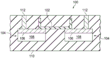
Fig. 3 illustrates an exemplary IC structure 100 including a Thin Film Resistor (TFR)102 formed in accordance with one embodiment of the present disclosure. TFR 102 may be formed within a polysilicon-metal dielectric (PMD) layer using a single added masking layer, for example, according to the exemplary damascene method discussed below with reference to fig. 4A-4K. As shown, TFR 102 extends between a pair of TFR headers 104 formed on field oxide 110. Each TFR header 104 may include a polysilicon region 106 having a silicide contact layer 106 formed on the polysilicon region 108, for example using a salicide (salicide) method, as described below. A conductive TFR via 112 may be connected to each silicide contact 106. In the illustrated example, the TFR 102 may be formed of SiCr, which may be annealed during fabrication to obtain a TCR of 0ppm or near 0 ppm.
Fig. 4A-4K illustrate an exemplary method for forming an exemplary IC structure having the Thin Film Resistor (TFR) shown in fig. 3, according to one exemplary embodiment. Fig. 4A illustrates the initial formation of an IC structure 200 by forming a pair of TFR headers 204 on a field oxide 210A. The TFR header 204 may be formed as a salicide (salicide polysilicon) structure that includes a silicide layer 206 on a polysilicon structure 208. The salicide structure 204 may include any suitable silicon-based chemistry, such as CoSi2、Co2Si, CoSi, NiSi, or TiSi2。
As shown in fig. 4B, the structure 200 may be further processed by depositing an additional silicon-based dielectric 210B on the structure, for example, using known HDP deposition methods. In one exemplary embodiment, the structure may include a 1K SRO (silicon rich oxide) deposition followed by a 10K HDP (high density plasma) deposition in region 210B.
As shown in fig. 4C, the structure 200 may be further processed by performing pre-metal dielectric chemical/mechanical planarization (PMDCMP) on the structure. In one exemplary embodiment, PMD CMP uses a target thickness of 6K on the active material (e.g., about 4K on each polysilicon structure 208).
As shown in fig. 4D, the structure 200 may be further processed by adding a sacrificial oxide layer 210C (e.g., about 1K thick) that may be subsequently polished away, as described below with respect to fig. 4I.
As shown in fig. 4E, the structure 200 may be further processed by depositing and patterning a photoresist layer 230 to form TFR trenches.
As shown in fig. 4F, the structure 200 may be further processed by etching the TFR trench 232 using any suitable etch process that may selectively stop on the silicide layer 206, and then the remaining photoresist material 230 may be removed, e.g., stripped.
As shown in fig. 4G, structure 200 may be further processed by: a layer of TFR material 240 is deposited over the structure and extends into the TFR trench 234, for example using a PVD or sputter deposition process. In one embodiment, TFR layer 240 may include a thickness of about (for example,
 ) A SiCr layer. In other implementations, the
 TFR layer 240 may include SiCCr, TaN, NiCr, AlNiCr, TiNiCr, or any other suitable TFR material.
The structure 200 including the TFR layer 240 may then be annealed, for example, at a temperature of about 500 ℃ (e.g., 400 ℃ -600 ℃ or 450 ℃ -550 ℃) to obtain a TCR (temperature coefficient of resistance) of the TFR layer 240 of 0ppm or close to 0 ppm. In some embodiments, according to specific embodiments, a "near 0" ppm TCR can include a TCR of 0 + -100 ppm/deg.C, or a TCR of 0 + -50 ppm/deg.C, or a TCR of 0 + -20 ppm/deg.C, or a TCR of 0 + -10 ppm/deg.C.
As shown in fig. 4H, the structure 200 may be further processed by depositing a cap oxide 210D on the structure 200 to protect the TFR film 240. The deposited cap oxide 210D may partially or completely fill the TFR trench 234. In one embodiment, the deposited cap oxide layer 210D has a thickness of about 4K.
As shown in fig. 4I, the structure 200 may be further processed by performing a polishing process to polish the cap oxide 210D, the portion of the layer of the TFR layer 240 outside the TFR trench 234, and the sacrificial oxide layer 210C to define a final TFR film structure 250. In one embodiment, the method may use the same target HDP thickness as shown in fig. 4C, such that the region of the wafer outside of the TFR module insertion location is the same as the region before TFR module formation begins (fig. 4C). In other words, TFR modules and manufacturing process steps may be modularized and may be added or omitted without changing the wafer or other parts of the process.
As shown in fig. 4J, the structure 200 may be further processed by depositing a phosphosilicate glass (PSG) layer or film 210E, and an Undoped Silicate Glass (USG) cap oxide layer 210F may be deposited on the structure. In one exemplary embodiment, the PSG 210E and USG 210F may each have a deposition thickness of about 2K.
As shown in fig. 4K, a pair of via-type contacts 260 connected to the TFR header 204 may be formed by patterning and etching the structure to define a pair of via openings, filling the via openings with a conductive material, such as tungsten (W), and performing a CMP process.
In this way, a TFR film incorporated in a PMD can be formed and connected between a pair of salicide TFR headers using a damascene method with a single mask layer. Further, in some embodiments, the TFR film may be formed of SiCr, which may be annealed to obtain a TCR of 0ppm or close to 0ppm, and the TFR may be used with both Cu and Al interconnects.
Thus, in contrast to some conventional techniques, in the disclosed embodiments, the TFR contacts are formed as part of a typical CMOS contact formation process, thereby eliminating one mask. In addition, the TFR header is a self-aligned polycide (polysilicon) structure formed in a typical CMOS process flow, which eliminates another mask. Thus, the TFR may be formed using only a single mask. Furthermore, the TFR may be formed by damascene (CMP), as opposed to wet or dry etching processes used in some conventional techniques.
Claims (20)
1. A method for fabricating a Thin Film Resistor (TFR) structure, the method comprising:
forming a pair of TFR headers spaced apart from each other, each TFR header including a salicide polysilicon (salicide) structure;
depositing a dielectric layer over the salicide TFR head;
patterning trenches into a photoresist layer using photolithography, the patterned trenches extending laterally over at least a portion of each salicide TFR head;
etching the trench through at least a portion of the dielectric layer and stopping at the salicide TFR heads such that a surface of each salicide TFR head is exposed; and
depositing a TFR material into the trench and onto an exposed surface of the salicide TFR head, forming a TFR layer bridging the pair of spaced apart salicide TFR heads.
2. The method of claim 1, wherein the TFR material comprises SiCr.
3. The method of any of claims 1-2, comprising annealing the structure after depositing the TFR material to change a Temperature Coefficient of Resistance (TCR) of the TFR material.
4. The method of claim 3, comprising annealing the structure to achieve a TCR of the TFR material of 0 + 100ppm/° C.
5. The method of claim 3, comprising annealing the structure to achieve a TCR of the TFR material of 0 + 50ppm/° C.
6. The method of claim 3, comprising annealing the structure to achieve a TCR of the TFR material of 0 + 10ppm/° C.
7. The method of any of claims 3-6, comprising annealing the structure at a temperature in a range of 450 ℃ to 550 ℃.
8. The method of any of claims 1-7, further comprising performing a Chemical Mechanical Polishing (CMP) process to remove portions of the TFR material outside the trench.
9. The method of claim 8, further comprising forming at least one of a phosphosilicate glass (PSG) layer or an Undoped Silicate Glass (USG) cap oxide layer over the structure after the removal process for removing the portion of the TFR material outside the trench.
10. The method of any of claims 1-9, further comprising forming a conductive contact to contact each salicide TFR head.
11. The method of any of claims 1-9, further comprising conductively connecting the TFR structure to at least one aluminum interconnect.
12. The method of any of claims 1-9, further comprising conductively connecting the TFR structure to at least one copper interconnect.
13. A Thin Film Resistor (TFR) structure, comprising:
a pair of spaced apart TFR headers, each TFR header including a salicide polysilicon (salicide) structure; and
a TFR layer in contact with each of the pair of salicide TFR headers, bridging the spaced apart salicide TFR headers;
wherein the salicide TFR head and the TFR layer are formed within a dielectric structure.
14. The TFR structure of claim 13, wherein the TFR material comprises SiCr.
15. The TFR structure of any of claims 13-14, wherein the TFR layer has a Temperature Coefficient of Resistance (TCR) of 0 ± 100ppm/° c resulting from annealing.
16. The TFR structure of any of claims 13-14, wherein the TFR layer has a Temperature Coefficient of Resistance (TCR) of 0 ± 50ppm/° c resulting from annealing.
17. The TFR structure of any of claims 13-14, wherein the TFR layer has a Temperature Coefficient of Resistance (TCR) of 0 ± 10ppm/° c resulting from annealing.
18. The TFR structure of any of claims 13-17, comprising at least one aluminum interconnect conductively coupled to the TFR structure.
19. The TFR structure of any of claims 13-17, comprising at least one copper interconnect conductively coupled to the TFR structure.
20. A Thin Film Resistor (TFR) structure formed by the method of any one of claims 1-12.
Applications Claiming Priority (5)
| Application Number | Priority Date | Filing Date | Title |
|---|---|---|---|
| US201762569261P | 2017-10-06 | 2017-10-06 | |
| US62/569,261 | 2017-10-06 | ||
| US16/037,941 | 2018-07-17 | ||
| US16/037,941 US10643887B2 (en) | 2017-10-06 | 2018-07-17 | Method of manufacturing damascene thin-film resistor (TFR) in poly-metal dielectric |
| PCT/US2018/053684 WO2019070551A1 (en) | 2017-10-06 | 2018-10-01 | Damascene thin-film resistor (tfr) in poly-metal dielectric and method of fabrication |
Publications (2)
| Publication Number | Publication Date |
|---|---|
| CN111052425A true CN111052425A (en) | 2020-04-21 |
| CN111052425B CN111052425B (en) | 2024-02-06 |
Family
ID=65994084
Family Applications (1)
| Application Number | Title | Priority Date | Filing Date |
|---|---|---|---|
| CN201880050912.6A Active CN111052425B (en) | 2017-10-06 | 2018-10-01 | Mosaic Thin Film Resistor (TFR) in polysilicon-metal dielectric and method of manufacture |
Country Status (5)
| Country | Link |
|---|---|
| US (1) | US10643887B2 (en) |
| CN (1) | CN111052425B (en) |
| DE (1) | DE112018004421B4 (en) |
| TW (1) | TW201926753A (en) |
| WO (1) | WO2019070551A1 (en) |
Cited By (1)
| Publication number | Priority date | Publication date | Assignee | Title |
|---|---|---|---|---|
| CN116325148A (en) * | 2021-02-23 | 2023-06-23 | 微芯片技术股份有限公司 | A TFR with a TFR element providing a diffusion barrier to the underlying thin film resistor (TFR) head |
Families Citing this family (4)
| Publication number | Priority date | Publication date | Assignee | Title |
|---|---|---|---|---|
| US11335635B2 (en) | 2020-04-08 | 2022-05-17 | Globalfoundries Singapore Pte. Ltd. | Thin film resistors of semiconductor devices |
| US11824079B2 (en) * | 2021-02-23 | 2023-11-21 | Microchip Technology Incorporated | Thin-film resistor (TFR) having a TFR element providing a diffusion barrier for underlying TFR heads |
| WO2023287457A1 (en) * | 2021-07-15 | 2023-01-19 | Microchip Technology Incorporated | Thin-film resistor (tfr) module |
| US11670439B2 (en) | 2021-07-15 | 2023-06-06 | Microchip Technology Incorporated | Thin-film resistor (TFR) module |
Citations (10)
| Publication number | Priority date | Publication date | Assignee | Title |
|---|---|---|---|---|
| US6426268B1 (en) * | 2000-11-28 | 2002-07-30 | Analog Devices, Inc. | Thin film resistor fabrication method |
| US6720249B1 (en) * | 2000-04-17 | 2004-04-13 | International Business Machines Corporation | Protective hardmask for producing interconnect structures |
| US20050218478A1 (en) * | 2004-03-23 | 2005-10-06 | Hirofumi Watanabe | Semiconductor device |
| US20060148228A1 (en) * | 2004-12-31 | 2006-07-06 | Bang Ki W | Method for forming salicide layer in semiconductor device |
| CN102324427A (en) * | 2011-10-20 | 2012-01-18 | 上海集成电路研发中心有限公司 | Metal film resistor structure and manufacturing method thereof |
| CN102376404A (en) * | 2010-08-24 | 2012-03-14 | 意法半导体有限公司 | Multi-layer via-less thin film resistor |
| CN103915382A (en) * | 2012-12-31 | 2014-07-09 | 德州仪器公司 | Embedded polysilicon resistor in integrated circuits formed by a replacement gate process |
| US20160218062A1 (en) * | 2015-01-23 | 2016-07-28 | Texas Instruments Incorporated | Thin film resistor integration in copper damascene metallization |
| US20160372420A1 (en) * | 2015-06-18 | 2016-12-22 | Microchip Technology Incorporated | Damascene Thin-Film Resistor with an Added Mask Layer |
| CN106463531A (en) * | 2014-06-18 | 2017-02-22 | 英特尔公司 | Pillar resistor structures for integrated circuitry |
Family Cites Families (8)
| Publication number | Priority date | Publication date | Assignee | Title |
|---|---|---|---|---|
| JP4141407B2 (en) * | 2003-06-11 | 2008-08-27 | 株式会社リコー | Manufacturing method of semiconductor device |
| US7112286B2 (en) | 2003-12-04 | 2006-09-26 | Texas Instruments Incorporated | Thin film resistor structure and method of fabricating a thin film resistor structure |
| US7999352B2 (en) * | 2004-02-19 | 2011-08-16 | Ricoh Company, Ltd. | Semiconductor device |
| US8563336B2 (en) * | 2008-12-23 | 2013-10-22 | International Business Machines Corporation | Method for forming thin film resistor and terminal bond pad simultaneously |
| US7960282B2 (en) | 2009-05-21 | 2011-06-14 | Globalfoundries Singapore Pte. Ltd. | Method of manufacture an integrated circuit system with through silicon via |
| US8530320B2 (en) * | 2011-06-08 | 2013-09-10 | International Business Machines Corporation | High-nitrogen content metal resistor and method of forming same |
| US9985088B2 (en) * | 2016-04-19 | 2018-05-29 | International Business Machines Corporation | Metal resistors having nitridized metal surface layers with different nitrogen content |
| US9991330B1 (en) * | 2017-01-11 | 2018-06-05 | International Business Machines Corporation | Resistors with controlled resistivity |
-
2018
- 2018-07-17 US US16/037,941 patent/US10643887B2/en active Active
- 2018-10-01 CN CN201880050912.6A patent/CN111052425B/en active Active
- 2018-10-01 WO PCT/US2018/053684 patent/WO2019070551A1/en not_active Ceased
- 2018-10-01 DE DE112018004421.1T patent/DE112018004421B4/en active Active
- 2018-10-04 TW TW107135023A patent/TW201926753A/en unknown
Patent Citations (10)
| Publication number | Priority date | Publication date | Assignee | Title |
|---|---|---|---|---|
| US6720249B1 (en) * | 2000-04-17 | 2004-04-13 | International Business Machines Corporation | Protective hardmask for producing interconnect structures |
| US6426268B1 (en) * | 2000-11-28 | 2002-07-30 | Analog Devices, Inc. | Thin film resistor fabrication method |
| US20050218478A1 (en) * | 2004-03-23 | 2005-10-06 | Hirofumi Watanabe | Semiconductor device |
| US20060148228A1 (en) * | 2004-12-31 | 2006-07-06 | Bang Ki W | Method for forming salicide layer in semiconductor device |
| CN102376404A (en) * | 2010-08-24 | 2012-03-14 | 意法半导体有限公司 | Multi-layer via-less thin film resistor |
| CN102324427A (en) * | 2011-10-20 | 2012-01-18 | 上海集成电路研发中心有限公司 | Metal film resistor structure and manufacturing method thereof |
| CN103915382A (en) * | 2012-12-31 | 2014-07-09 | 德州仪器公司 | Embedded polysilicon resistor in integrated circuits formed by a replacement gate process |
| CN106463531A (en) * | 2014-06-18 | 2017-02-22 | 英特尔公司 | Pillar resistor structures for integrated circuitry |
| US20160218062A1 (en) * | 2015-01-23 | 2016-07-28 | Texas Instruments Incorporated | Thin film resistor integration in copper damascene metallization |
| US20160372420A1 (en) * | 2015-06-18 | 2016-12-22 | Microchip Technology Incorporated | Damascene Thin-Film Resistor with an Added Mask Layer |
Non-Patent Citations (1)
| Title |
|---|
| YOUNG-CHEON KWON: ""Process Optimization of Integrated SiCr Thin-Film Resistor for High-Performance Analog Circuits"" * |
Cited By (1)
| Publication number | Priority date | Publication date | Assignee | Title |
|---|---|---|---|---|
| CN116325148A (en) * | 2021-02-23 | 2023-06-23 | 微芯片技术股份有限公司 | A TFR with a TFR element providing a diffusion barrier to the underlying thin film resistor (TFR) head |
Also Published As
| Publication number | Publication date |
|---|---|
| US10643887B2 (en) | 2020-05-05 |
| DE112018004421B4 (en) | 2024-08-08 |
| US20190109186A1 (en) | 2019-04-11 |
| CN111052425B (en) | 2024-02-06 |
| TW201926753A (en) | 2019-07-01 |
| DE112018004421T5 (en) | 2020-05-20 |
| WO2019070551A1 (en) | 2019-04-11 |
Similar Documents
| Publication | Publication Date | Title |
|---|---|---|
| CN112335065B (en) | Thin film resistor in integrated circuit and method for manufacturing the same | |
| CN111052425B (en) | Mosaic Thin Film Resistor (TFR) in polysilicon-metal dielectric and method of manufacture | |
| CN112119511B (en) | Thin film resistor in integrated circuit and manufacturing method | |
| US10546813B2 (en) | BEOL vertical fuse formed over air gap | |
| CN107750390B (en) | Damascene thin film resistor with increased mask layer | |
| CN112313809B (en) | Aluminum compatible thin film resistor (TFR) and method for manufacturing the same | |
| CN108028253B (en) | Method and design of low sheet resistance MEOL resistor | |
| CN117497513A (en) | Semiconductor devices and methods of forming the same | |
| US6737326B2 (en) | Method of integrating a thin film resistor in a multi-level metal tungsten-plug interconnect | |
| TW201919147A (en) | Systems and methods for forming a thin film resistor integrated in an integrated circuit device | |
| KR100852207B1 (en) | Removing insulating film and forming metal wiring | |
| US20150262911A1 (en) | Tsv with end cap, method and 3d integrated circuit | |
| US11670439B2 (en) | Thin-film resistor (TFR) module | |
| US10566411B2 (en) | On-chip resistors with direct wiring connections | |
| US20010044202A1 (en) | Method of preventing copper poisoning in the fabrication of metal interconnects | |
| CN113728448B (en) | Forming Thin Film Resistors (TFRs) in Integrated Circuit Devices | |
| CN116325148A (en) | A TFR with a TFR element providing a diffusion barrier to the underlying thin film resistor (TFR) head | |
| US9202758B1 (en) | Method for manufacturing a contact for a semiconductor component and related structure | |
| WO2023287457A1 (en) | Thin-film resistor (tfr) module | |
| KR101138063B1 (en) | Metal wiring formation method of semiconductor device | |
| CN118302857A (en) | A TFR module including a thin film resistor (TFR) element formed in a metal cup structure |
Legal Events
| Date | Code | Title | Description |
|---|---|---|---|
| PB01 | Publication | ||
| PB01 | Publication | ||
| SE01 | Entry into force of request for substantive examination | ||
| SE01 | Entry into force of request for substantive examination | ||
| GR01 | Patent grant | ||
| GR01 | Patent grant |