Preparation method of LED light-emitting device
Technical Field
The invention relates to a preparation method of an LED light-emitting device.
Background
COB encapsulation can be with a plurality of LED chip direct packaging on printed circuit board, and COB encapsulated LED illuminator includes a plurality of LED chips of installation on the base plate, and the use of a plurality of LED chips not only can improve luminance, still helps realizing the reasonable configuration of LED chip, reduces the input current volume of single LED chip in order to ensure high efficiency. When the substrate is used for a long time, the plurality of LED chips emit a large amount of heat, which requires the substrate to have good heat dissipation performance.
In order to make the substrate have good heat dissipation performance, a metal substrate can be adopted, but because the reflectivity of the metal surface is not high, the light emitted by the side surface of the LED chip is absorbed by the metal surface, so that the light emitting efficiency of the LED module is low. To increase the reflectivity of the LED chip, it may be mounted on a film layer of a material having a high reflectivity.
Chinese published patent application CN101866108A discloses a solder resist film which is a photocurable and thermosetting composition formed by adding rutile titanium oxide as a white pigment to an epoxy composition and can withstand long-term use without deterioration. The composition has high reflectivity but no good heat dissipation performance, and a plurality of LED chips directly mounted on the composition can generate more heat and are difficult to dissipate after being used for a long time.
Therefore, a manufacturing method is needed to make the LED light emitting device have both good heat dissipation performance and high reflectivity, i.e. the heat generated by the LED chip can be effectively dissipated, and the LED light emitting device has high light emitting efficiency.
Disclosure of Invention
In view of the defects of the prior art, the main object of the present invention is to provide a method for manufacturing an LED light emitting device with good heat dissipation performance and high light extraction efficiency.
In order to achieve the above main object, the present invention provides a method for manufacturing an LED light emitting device, wherein the LED light emitting device includes an LED package member and a circuit board, and the circuit board includes an insulating substrate and a metal heat sink. The preparation method comprises the following steps:
step A: processing the insulating substrate to form a hole for the metal radiator to pass through;
and B: enabling the metal radiator to penetrate through the hole, and to be bonded with the insulating substrate through the adhesive material, and enabling the upper surface of the metal radiator to be flush with the metal layer on the upper surface of the insulating substrate;
and C: simultaneously etching the metal layer on the upper surface of the insulating substrate and the upper surface of the metal radiator to form a conducting circuit pattern on the upper surface of the insulating substrate, and forming a concave area and an unetched mounting area covered by the mask on the upper surface of the metal radiator;
step D: filling white reflective materials in the concave area;
step E: installing LED chips in the installation area, and enabling the LED chips and the conducting circuit patterns to form required electric connection through metal leads;
step F: the LED chips and the metal leads among the LED chips are packaged together by packaging materials to form an LED packaging component.
According to the scheme, the LED chip is arranged in the mounting area of the metal radiator in the LED light-emitting device manufactured by the manufacturing method, so that heat generated by the LED chip can be effectively dissipated, light emitted from the side surface of the LED chip is reflected by the white reflecting material in the concave area, and the LED light-emitting device has high light-emitting efficiency. The metal layer on the upper surface of the insulating substrate and the upper surface of the metal radiator are etched simultaneously, so that the production process is simplified, the time is saved, and the cost is saved.
More specifically, the white light reflecting material filled in step D is a white ink composition containing a white pigment, and the white pigment includes titanium oxide powder. Titanium oxide is used as a white pigment to improve the reflection performance of the white insulating material.
More specifically, in the step D, the white ink composition is filled into the concave region by adopting a screen printing mode. Accurate filling of the recessed areas with white reflective material can be achieved with screen printing.
In another more specific embodiment, the white ink composition is allowed to sufficiently fill the recessed region while the step D is performed. The filling process is repeated until the white ink composition completely fills the recessed area.
More specifically, the preparation method further comprises the step of polishing after the step D is finished and the white ink composition is cured, so that the upper surface of the white ink composition is flush with the upper surface of the metal radiator. The upper surface of the white reflecting material is flush with the upper surface of the metal radiator, so that light emitted from the side surface of the LED chip is completely reflected by the white reflecting material, and the LED chip has high light-emitting efficiency.
And D, after the step C is finished, etching the upper surface of the metal heat radiator into mutually separated mounting areas for mounting the LED chip. The mounting areas are separated from each other, so that the LED chips mounted on the mounting areas can effectively dissipate heat, and light emitted by the side surfaces of the mounting areas is reflected by the white insulating material in the recessed areas, so that the circuit board is ensured to have higher reflectivity.
More specifically, the mounting region has a cross section corresponding to the bottom surface of the LED chip. The arrangement can ensure that the mounting area does not influence the light emitted by the side surface of the LED chip and fully exert the heat radiation performance of the metal heat radiation body.
In another more specific aspect, the recessed region has a depth of 0.5mm to 3mm after step C is completed. So that the white reflecting material can fully exert the reflecting performance.
Preferably, step a further includes a step of processing a second hole required for forming the conductive via hole, and electroplating is performed after the insulating substrate and the metal heat spreader are bonded together, so as to form a conductive metal layer in the second hole. Through the conductive vias, electrical connections can be made to the conductive pattern lines on the upper surface of the insulating substrate to electrically connect to the inner patterned metal layer or the lower patterned metal layer of the insulating substrate.
More specifically, the conductive via penetrates through the insulating substrate, and the preparation method further comprises the step of forming a patterned second metal layer electrically connected with the conductive via on the lower surface of the insulating substrate. The second metal layer may include electrodes to electrically connect with other components.
To more clearly illustrate the objects, technical solutions and advantages of the present invention, the present invention will be further described in detail with reference to the accompanying drawings and detailed description.
Drawings
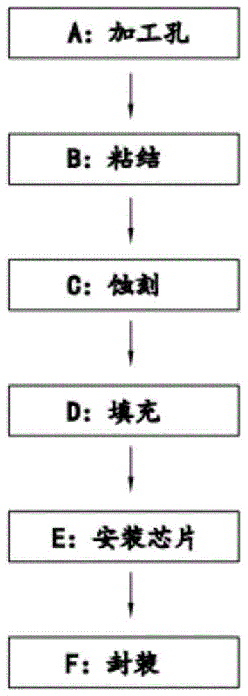
FIG. 1 is a process flow diagram of example 1 of the present invention;
FIG. 2 is a schematic structural diagram of a product after completion of step A in example 1 of the present invention;
FIG. 3 is a schematic structural diagram of a product after completion of step B in example 1 of the present invention;
FIG. 4 is a schematic structural diagram of a product after completion of step C in example 1 of the present invention;
fig. 5 is a schematic structural diagram of the upper surface of the metal heat sink after step C in embodiment 1 of the present invention is completed;
FIG. 6 is a schematic structural diagram of a product after completion of step D in example 1 of the present invention;
FIG. 7 is a schematic structural view of a product obtained by grinding after step D in example 1 of the present invention;
fig. 8 is a schematic structural diagram of a product after the LED chip is mounted in step E in embodiment 1 of the present invention;
FIG. 9 is a schematic structural view of a product after completion of step F in example 1 of the present invention;
FIG. 10 is a schematic structural view of a product after completion of step A in example 2 of the present invention;
FIG. 11 is a schematic structural diagram of a product after completion of step B in example 2 of the present invention;
FIG. 12 is a schematic structural diagram of a product after completion of step F in example 2 of the present invention.
Detailed Description
Example 1
As shown in fig. 1, the method for manufacturing an LED light emitting device according to the embodiment of the present invention includes step A, B, C, D, E, F, where the step a is to process a hole on the insulating substrate, where the hole is capable of at least partially accommodating a metal heat sink, so that the metal heat sink can penetrate from the lower surface of the insulating substrate to the upper surface of the insulating substrate; step B, bonding refers to bonding the insulating substrate and the metal radiator together through an adhesive material; step C, etching refers to etching the metal layer on the upper surface of the insulating substrate and etching the upper surface of the metal radiator simultaneously to enable the metal layer to form a conductive circuit pattern, a concave area is formed on the upper surface of the metal radiator, and a mounting area is formed on the part which is not etched; step D, filling, namely filling white reflective materials in the concave area; step E, installing the LED chips in the installation area, and enabling the LED chips and the conducting circuit patterns to form required electric connection through metal leads; and step F, packaging the LED chips and the metal leads among the LED chips together by using packaging materials to form an LED packaging structure.
Fig. 2 schematically shows an insulating substrate of one configuration. As shown in fig. 2, the insulating substrate includes two insulating medium layers 11 and 12, wherein the upper insulating medium layer has a metal layer 41 thereon, an adhesive material 31 is disposed between the insulating medium layers 11 and 12, and a hole 20' is formed to accommodate the metal heat sink.
In the bonding step B, the insulating substrate 10 and the metal heat spreader 20 may be bonded together using the same adhesive material 32 as the adhesive material 31, and in the case of using the same material, the step of bonding the insulating medium layers to each other may be performed together with the step of bonding the metal heat spreader and the insulating substrate, or a different adhesive material may be used to form the structure shown in fig. 3.
Then, an appropriate mask is put on the upper surfaces of the metal layer 41 and the metal heat radiator 20 to perform step C simultaneously. After the etching is completed, the product shown in fig. 4 is produced, the metal layer 41 forms a desired conductive circuit pattern, and the upper surface of the metal heat sink forms a recessed area 212, preferably, the depth of the recessed area is 0.5mm to 3 mm. The structure of the etched upper surface of the metal heat sink is shown in fig. 5, the upper surface of the metal heat sink is partitioned by the recessed area 212 into a plurality of mounting areas 211 which are distributed in a staggered manner and spaced apart from each other, and the size of the mounting areas can be consistent with the bottom surface of the LED chip to be mounted thereon.
And D, filling a white light reflecting material in the concave area. The white light reflecting material may be a white ink composition containing a white pigment, and the white pigment may be titanium oxide or other substances capable of increasing the reflectivity of the composition. The filling process may be applied by screen printing or other means. This process may be performed multiple times so that the white light reflecting material 213 substantially fills the recessed area, as shown in fig. 6.
After filling, the top of the white reflective material can be polished to make the upper surface of the white reflective material flush with the upper surface of the metal heat sink. At the same time, the exposed adhesive material portion during etching can be polished away to form the structure shown in fig. 7.
Step E is then performed, as shown in fig. 8, to mount the LED chips on the mounting area and to form the desired electrical connections between the LED chips and the conductive line pattern via the metal leads 71.
Finally, step F is performed to package the LED chips and their metal leads with each other by using a packaging material 61 to form an LED package member as shown in fig. 9. The encapsulating material is required to have high light transmittance and good high temperature resistance, such as modified epoxy resin, silicone material, and the like. In order to change the color of light emitted by the LED chip, a phosphor may be added into the encapsulant, for example, the LED chip emitting blue light may generate white light after passing through the encapsulant containing a specific phosphor.
When the LED light-emitting device manufactured according to the method of the present embodiment is used, since the mounting region has a cross section equivalent to that of the LED chip, the lower surface of the LED chip is completely in direct or indirect contact with the metal heat sink, and heat generated by the LED chip in the use process is sufficiently transferred to the upper surface of the metal heat sink through the lower surface of the LED chip and dissipated through the metal heat sink. Most of the light emitted by the LED chip is emitted through the upper surface of the LED chip, and the light emitted from the side surface and irradiated to the circuit board is reflected by the white insulating material and also emitted from the upper surface of the circuit board. Because the upper surface of white reflecting material and the upper surface parallel and level of metal radiator, after installing the LED chip, the metal radiator does not expose from the upper surface of circuit board to the light that the LED chip dispersed to the circuit board can not be absorbed by the metal radiator and totally reflected by white insulating material, and luminous efficacy is high. The lower part of the metal heat radiator completely supports the insulating substrate, so that heat generated by the insulating substrate, and electronic devices and conducting circuits on the insulating substrate during working can be transferred to the metal heat radiator through the lower surface of the insulating substrate, and the whole LED light-emitting device has good heat radiation performance.
In other embodiments, the insulating substrate may further include an intermediate metal layer disposed between the two insulating dielectric layers, and the intermediate metal layer may have an inner conductive line.
Example 2
In this embodiment, similar to embodiment 1, the electrode on the lower surface of the package structure and the conductive via hole for electrically connecting the electrode and the patterned metal layer on the upper surface are added to the manufactured product structure, which adds some processes compared with embodiment 1, and the rest steps are basically the same.
As shown in fig. 10, when the hole 20 'is formed, a hole 50' is formed to penetrate the insulating medium layers 11 and 12, the adhesive layer 31, and the metal layer 41 of the insulating substrate 10. Then, a bonding step is performed, and a plating step is added after the bonding is completed to form a metal layer 51 in the conductive via 50, and then the metal layer 51 is filled with an insulating material 52 to form a product structure as shown in fig. 11. In addition, the lower surface of the insulating substrate has a metal layer which is also etched to form a conductive pattern including the electrode 42. The resulting LED lighting device is shown in fig. 12.
Although the present invention has been described with reference to specific embodiments, it is not intended to limit the scope of the invention. It will be appreciated by those skilled in the art that changes may be made without departing from the scope of the invention, and it is intended that all matter contained in the above description or shown in the accompanying drawings shall be interpreted as illustrative and not in a limiting sense.