CN1111407A - high voltage equipment - Google Patents
high voltage equipment Download PDFInfo
- Publication number
- CN1111407A CN1111407A CN94113368A CN94113368A CN1111407A CN 1111407 A CN1111407 A CN 1111407A CN 94113368 A CN94113368 A CN 94113368A CN 94113368 A CN94113368 A CN 94113368A CN 1111407 A CN1111407 A CN 1111407A
- Authority
- CN
- China
- Prior art keywords
- filler
- voltage equipment
- equipment according
- protective
- protective layer
- Prior art date
- Legal status (The legal status is an assumption and is not a legal conclusion. Google has not performed a legal analysis and makes no representation as to the accuracy of the status listed.)
- Granted
Links
Images

Classifications
-
- H—ELECTRICITY
- H02—GENERATION; CONVERSION OR DISTRIBUTION OF ELECTRIC POWER
- H02G—INSTALLATION OF ELECTRIC CABLES OR LINES, OR OF COMBINED OPTICAL AND ELECTRIC CABLES OR LINES
- H02G5/00—Installations of bus-bars
- H02G5/06—Totally-enclosed installations, e.g. in metal casings
- H02G5/063—Totally-enclosed installations, e.g. in metal casings filled with oil or gas
- H02G5/065—Particle traps
-
- Y—GENERAL TAGGING OF NEW TECHNOLOGICAL DEVELOPMENTS; GENERAL TAGGING OF CROSS-SECTIONAL TECHNOLOGIES SPANNING OVER SEVERAL SECTIONS OF THE IPC; TECHNICAL SUBJECTS COVERED BY FORMER USPC CROSS-REFERENCE ART COLLECTIONS [XRACs] AND DIGESTS
- Y10—TECHNICAL SUBJECTS COVERED BY FORMER USPC
- Y10T—TECHNICAL SUBJECTS COVERED BY FORMER US CLASSIFICATION
- Y10T428/00—Stock material or miscellaneous articles
- Y10T428/23—Sheet including cover or casing
- Y10T428/239—Complete cover or casing
-
- Y—GENERAL TAGGING OF NEW TECHNOLOGICAL DEVELOPMENTS; GENERAL TAGGING OF CROSS-SECTIONAL TECHNOLOGIES SPANNING OVER SEVERAL SECTIONS OF THE IPC; TECHNICAL SUBJECTS COVERED BY FORMER USPC CROSS-REFERENCE ART COLLECTIONS [XRACs] AND DIGESTS
- Y10—TECHNICAL SUBJECTS COVERED BY FORMER USPC
- Y10T—TECHNICAL SUBJECTS COVERED BY FORMER US CLASSIFICATION
- Y10T428/00—Stock material or miscellaneous articles
- Y10T428/30—Self-sustaining carbon mass or layer with impregnant or other layer
-
- Y—GENERAL TAGGING OF NEW TECHNOLOGICAL DEVELOPMENTS; GENERAL TAGGING OF CROSS-SECTIONAL TECHNOLOGIES SPANNING OVER SEVERAL SECTIONS OF THE IPC; TECHNICAL SUBJECTS COVERED BY FORMER USPC CROSS-REFERENCE ART COLLECTIONS [XRACs] AND DIGESTS
- Y10—TECHNICAL SUBJECTS COVERED BY FORMER USPC
- Y10T—TECHNICAL SUBJECTS COVERED BY FORMER US CLASSIFICATION
- Y10T428/00—Stock material or miscellaneous articles
- Y10T428/31504—Composite [nonstructural laminate]
- Y10T428/31678—Of metal
- Y10T428/31703—Next to cellulosic
Landscapes
- Chemical & Material Sciences (AREA)
- Oil, Petroleum & Natural Gas (AREA)
- Organic Insulating Materials (AREA)
- Installation Of Bus-Bars (AREA)
- Laminated Bodies (AREA)
- Insulating Bodies (AREA)
- Driving Mechanisms And Operating Circuits Of Arc-Extinguishing High-Tension Switches (AREA)
- Insulators (AREA)
- Casings For Electric Apparatus (AREA)
Abstract
一种高压设备,具有内部充有绝缘气体的金属外 壳,外壳内容纳着承压的有源部件。此外,在外壳(1) 的内表面上或在有源部件的外表面上至少有一至少 为局部敷设的保护涂层(7,9,10),或者在外壳(1)的 内表面和有源部件的外表面上都至少有一至少为局 部敷设的保护层,此保护层上掺杂有至少一种填充 剂,这种填充剂可吸收自由电子,从而提高高压设备 的绝缘水平。
A high voltage device having a metal enclosure filled with an insulating gas inside which houses pressurized active components. In addition, there is at least an at least partially applied protective coating (7, 9, 10) on the inner surface of the housing (1) or on the outer surface of the active components, or on the inner surface of the housing (1) and the active The outer surfaces of the components each have at least one at least partially applied protective layer, which is doped with at least one filler which absorbs free electrons and thus increases the insulation level of the high-voltage device.
Description
本发明涉及一种高压设备。The invention relates to a high voltage device.
已知的高压设备包括一内部充有例如SF6的绝缘气体的接地金属壳体,所述壳体的与传导高压的有源部件相对置的内表面上带有保护性涂层。这个保护层使该表面变得光滑,特别是利于清洁,而不会出现粗糙表面残留纤维或其它清洗媒介物的余渣的问题,这些残留物导致绝缘气体间隙的绝缘强度下降。在这种设备的有源部件表面上也常常带有同样的保护层。Known high-voltage equipment comprises a grounded metal enclosure filled with an insulating gas, such as SF6, with a protective coating on the inner surface of the enclosure opposite the active components conducting the high voltage. This protective layer makes the surface smooth and in particular facilitates cleaning without the problem of residues of fibers or other cleaning media remaining on the rough surface, which residues lead to a reduction in the dielectric strength of the insulating gas gap. The same protective layer is often present on the surfaces of the active components of such devices.
DE 41 20 309 A1公开了一种高压设备,它的金属外壳内充有绝缘气体,输送电压的有源部件装在此壳体内。在该壳体的内表面上和有源部件的外表面上带有保护性涂层。在这种高压设备中,由于自由漂移的或固定不动的粒子的存在,使绝缘气体间隙的绝缘强度下降,但其程度受到限制,因为特别加有保护涂层,并且至少部分地涂覆了第二保护涂层。导电粒子在这种高压设备中的运动并无规则。此外,与没有加所述涂层的表面相比较,由导电粒子引起的粒子放电强度显著减弱。但是,在这种高压设备中的自由电子并非规则可靠地活动,它们会具有不利的影响。如果在表面的附近所产生的电子是在尖状物上局部放电的结果或是粒子被捕获的结果,则绝缘气体间隙的绝缘强度可获得改善。此外,采用第二保护涂层成本较高。DE 41 20 309 A1 discloses a high-voltage device whose metal casing is filled with an insulating gas and in which the active components for delivering the voltage are housed. A protective coating is provided on the inner surface of the housing and on the outer surface of the active components. In such high-voltage equipment, the dielectric strength of the insulating gas gap is reduced, but to a limited extent, due to the presence of freely drifting or immobile particles, because a protective coating is especially applied and at least partially coated Second protective coat. The movement of conductive particles in this high-voltage device is irregular. In addition, the particle discharge intensity caused by the conductive particles is significantly reduced compared to a surface without said coating. However, free electrons in such high-voltage devices do not move regularly and reliably, and they can have adverse effects. The dielectric strength of the insulating gas gap can be improved if electrons are generated in the vicinity of the surface as a result of partial discharges on the spikes or as a result of particles being trapped. In addition, the use of a second protective coating is costly.
因此,本发明的一个目的是提供一种高压设备,它使自由电子从绝缘间隙中能可靠地脱离,并且可将由自由粒子产生的局部放电现象减小到非临界的强度值。It is therefore an object of the present invention to provide a high-voltage device which enables reliable escape of free electrons from insulating gaps and which reduces partial discharge phenomena caused by free particles to non-critical intensity values.
本发明所获得的效果主要体现在:由开关过程或放电过程所产生的自由电子在其引起闪络击穿之前已由填充剂所捕获和吸收。The effect obtained by the present invention is mainly reflected in that the free electrons generated by the switching process or the discharging process have been captured and absorbed by the filler before they cause flashover breakdown.
这种高压设备具有金属外壳,内部充有绝缘气体,壳体包围着传输电压的有源部件。在外壳的内表面上或在有源部件的外表面上至少加有一局部涂层,或者在外壳的内表面上和有源部件的外表面上都附加至少一个至少是局部覆盖的保护涂层。至少一个保护层内搀杂有至少一种填充剂。This high-voltage device has a metal casing filled with an insulating gas that encloses the active components that transmit the voltage. At least one partial coating is applied to the inner surface of the housing or to the outer surface of the active component, or at least one at least partially covering protective coating is applied to both the inner surface of the housing and the outer surface of the active component. At least one protective layer is doped with at least one filler.
这种保护涂层可直接在合适的表面上进行汽相淀积形成,它包括至少一种填充剂。然而,该保护涂层也可使用搀杂有至少一种填充剂的涂漆表面形成,这里漆可以用环氧树脂漆或基于聚乙烯的漆。The protective coating may be formed by vapor deposition directly on the suitable surface and includes at least one filler. However, the protective coating can also be formed using a painted surface doped with at least one filler, where the paint can be an epoxy resin paint or a polyethylene based paint.
如果将至少一种填充剂集中到漆或保护层的表面上,则可产生特别好的效果。Particularly good results can be produced if at least one filler is concentrated on the surface of the lacquer or protective layer.
最好采用C60作为填充剂之一。然而,也可使用具有较大分子的填充剂。It is best to use C60 as one of the fillers. However, fillers with larger molecules may also be used.
所附的权利要求进一步补充和完善了本发明。The invention is further supplemented and completed by the appended claims.
通过下面结合附图的详细描述可更清楚全面地了解本发明的附加的内容和许多有益效果,该附图展示了一种实施方法,其中:The additional content and many beneficial effects of the present invention can be more clearly and comprehensively understood through the following detailed description in conjunction with the accompanying drawings. This accompanying drawing shows a method of implementation, wherein:
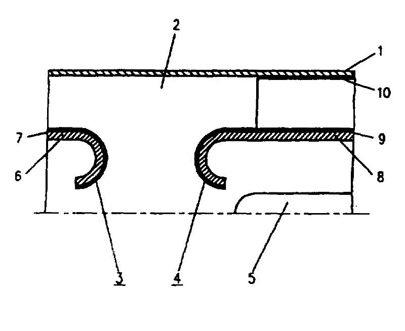
这张唯一附图表示本发明的高压设备的一个局部视图。The single figure shows a partial view of the high-voltage system according to the invention.
现在参看附图,该图表示本发明的高压设备的一个局部。一个大致为圆筒形的耐压的金属外壳1包容着一个充有SF6绝缘气体的内部空间2。有源部件位于外壳1的中心,图中只以简化形式表示出一个开关点。在开关点的一侧为图中未示出的固定触头,其上集中地环绕有一屏蔽3。在屏蔽3内还装有用于传导额定电流的触头(图中未示出)。在开关点的另一侧是动触头5和集中地环绕住动触头的屏蔽4,图中所示为开关断开位置,用于转送额定电流所需的触头位于屏蔽4内,图中也未示出。这一图示的开关点可以是断路器的一部分,也可是绝缘子或负荷开关或接地开关或接地绝缘子的一部分。Referring now to the drawings, there is shown a portion of the high voltage apparatus of the present invention. A roughly cylindrical pressure-
屏蔽3是由金属板6制成,其上覆盖着一保护层7,该保护层7面向外壳1的表面侧并且面向相对设置的屏蔽4。屏蔽4由金属板8制成,它的面向外壳1的表面上和相对着位于对侧的屏蔽3的表面上覆盖着一保护层9。外壳1的内表面也完全地或局部地覆盖着保护层10。这些保护层7,9和10包括一种加入填充剂的环氧树脂漆的基本材料,在此情况下,具体地是C60被引入。也可使用以聚乙烯为基的漆作为基本材料。这种填充料的制造可参见美国US5,227,038号专利说明书。除了这种填加剂外,也可使用导电的或半导体的掺杂,例如TiO2成份或导电涂料Al2O3或各种物质的混合物,这些添加料是用于保护涂层的标准材料。此外,其他一些导电物质也可用于制造所述涂层。在这种情况下,这种导电的保护层使所涂覆的部件表面变成不导电的平滑的表面。由于这些部件位于导电的或不导电的活性保护层内,因此任何略微突出于其表面上的细小尖状部位不再对绝缘构成不利影响。The
可以在外壳1的内表面上和有源部件的外表面上整体地涂上述保护涂层。也可以只在高压设备的一个区域上或多个区域上提供所述保护涂层,并且,尤其是在那些开关气体或其他开关沉积物可能出现之处设置该保护层,不过对某些应用情况,只在有源部件上覆盖保护层就足以满足要求,特别是可在高压设备的一或多个区域上敷设。The above-mentioned protective coating can be integrally applied on the inner surface of the
如果填充剂集中在漆层表面上,将使该填充剂发挥出色的高效率。填充剂C60特别适于用在高压设备中,因为它对自由电子具有良好的吸收性。此外,它的制备比较简单,因此对技术应用场合有很好的适应性。在这种情况下也可以采用碳原子含量高于C60的填充剂。If the filler is concentrated on the surface of the paint layer, it will make the filler work at an excellent high efficiency. Filler C60 is particularly suitable for use in high-voltage equipment because of its good absorption of free electrons. In addition, it is relatively simple to prepare and therefore has good adaptability to technical applications. Fillers with a higher carbon atom content than C60 can also be used in this case.
直接在适当的表面上汽相淀积的填充层包括至少一种填充剂,这种填充层可用作保护涂层7,9,10。在这种情况下,在汽相淀积填充剂之前,常常将以环氧树脂为基的粘合剂施加到所述表面上作为附加的粘合层。这样,在填充剂分子与适当表面之间形成一种特殊的薄膜连接。如果采用单组分的粘合剂作为粘合剂,则使保护层的形成工艺特别简单。CIBA-GEIGY公司的单组分粘合剂Araldite AV 119(Araldite是CIBA-GEIGY公司的注册商标)由于具有触变性,可被特别容易地加工。由于汽相淀积是在较高温度下进行的,在这一加工过程中,单组分粘合剂Araldite AV 119基本上固化。但是其固化程度尚不够,还需放入炉中额外处理后实现固化。Filling layers vapor-deposited directly on suitable surfaces comprising at least one filler can be used as
在生产所述保护涂层7,9,10时,在应用单成组粘合剂Araldite AV 119作为附加粘合层之前,一般应将金属表面快速喷砂处理,以便在有关的表面上获得一具有良好粘结特性的粘附层。在喷砂后,利用诸如丙酮或三氯乙烯的油脂溶剂对该粗糙的表面进行化学去脂。之后,将单组分粘合剂Araldite AV 119均匀地涂布到已去脂的表面上。这种单组分粘合剂Araldite AV 119是基于双酚A形成的环氧树脂粘合剂,它加工简单并不出现滴流现象。When producing said protective coating7,9,10, the metal surface should generally be blasted quickly before applying the single-pack adhesive Araldite AV 119 as an additional adhesive layer in order to obtain a Adhesive layer with good bonding properties. After blasting, the rough surface is chemically degreased using a grease solvent such as acetone or trichloroethylene. Afterwards, apply the one-component adhesive Araldite AV 119 evenly to the degreased surface. The one-component adhesive Araldite AV 119 is an epoxy resin adhesive based on bisphenol A, which is easy to process and does not appear to drip.
在该表面和粘着层的接合处之间的表面上可能会出现尖峰放电,并引起电场失真。为消除这一电场失真,可将单组分粘合剂掺杂一些导电的或半导体的粉末,从而以这种方式避免了在此区域的粘合剂层在等电位表面内出现电场失真,以这种方式,还可避免在此区域内发生局部放电现象。Spike discharges may occur on the surface between this surface and the junction of the adhesive layer and cause distortion of the electric field. In order to eliminate this electric field distortion, the one-component adhesive can be doped with some conductive or semiconducting powders, thus avoiding the electric field distortion in the equipotential surface of the adhesive layer in this area in this way, so as to In this way, partial discharge phenomena can also be avoided in this area.
下面更详细地结合附图说明本发明的作用方式。如果高压设备承载有电压,如果开关点处于断开位置,如图中所示,自由电子总是由电离辐射产生,以及由自由运动的或固定的粒子的局部放电产生。以这种方式产生的自由电子可进一步产生自由电子雪崩,而且在不利的情况下,例如设备的绝缘水平已由于过载的拖累而出现减弱,则可能在有源部件和接地外壳1之间产生击穿闪络现象。只有当这些自由电子由存在于保护层7,9内的填充剂所吸收并在其产生后立即被变为无害的情况下,才能完全避免所述闪络现象。The action mode of the present invention will be described in more detail below in conjunction with the accompanying drawings. If the high-voltage equipment is carrying a voltage, if the switching point is in the off position, as shown in the figure, free electrons are always generated by ionizing radiation, as well as by partial discharges of freely moving or stationary particles. The free electrons generated in this way can further generate an avalanche of free electrons and, in unfavorable cases, e.g. if the insulation level of the device has weakened due to overload encumbrance, can produce shocks between active components and grounded
如果将传统的高压设备系统化地加装这些含有填充剂的保护涂层7,9,10,则使所述高压设备的操作安全性得以极大提高。If conventional high-voltage equipment is systematically equipped with these filler-containing
如果以往的安全极限认为是足够的,则相对于等量的传统的高压设备的尺寸而言,带有填充剂的保护层7,9,10的高压设备的尺寸可大大减小,这将取得显著的经济效益。If previous safety limits are considered adequate, the size of high voltage equipment with filler
当含有填充剂的保护层7,9,10和在开关操作期间及由自由电子产生的气体云之间相接触时,这些涂层仍具有优良的性能。保护层或填充剂吸收所述自由电子,从而增大了屏蔽3和4之间及开关触头间的绝缘阻抗。这加快了开关断点的绝缘恢复能力,使所述开关的遮断容易提高,或者说开关的安全性增强。These coatings still have good properties when there is contact between the filler-containing
虽然,在本发明的教导下,完全可以作出本发明的各种完善和改变。可以认为,这些在实践本发明中得出的并未在此专门说明的改进均在所附的权利要求范围内。Although, under the teaching of the present invention, various improvements and changes of the present invention can be made fully. Such modifications in the practice of the invention not specifically described herein are considered to be within the scope of the appended claims.
Claims (10)
Applications Claiming Priority (2)
| Application Number | Priority Date | Filing Date | Title |
|---|---|---|---|
| DEP4344764.3 | 1993-12-28 | ||
| DE4344764A DE4344764A1 (en) | 1993-12-28 | 1993-12-28 | High voltage system |
Publications (2)
| Publication Number | Publication Date |
|---|---|
| CN1111407A true CN1111407A (en) | 1995-11-08 |
| CN1041982C CN1041982C (en) | 1999-02-03 |
Family
ID=6506423
Family Applications (1)
| Application Number | Title | Priority Date | Filing Date |
|---|---|---|---|
| CN94113368A Expired - Fee Related CN1041982C (en) | 1993-12-28 | 1994-12-28 | High-voltage installation |
Country Status (9)
| Country | Link |
|---|---|
| US (1) | US5558915A (en) |
| EP (1) | EP0661788B1 (en) |
| JP (1) | JPH07220586A (en) |
| CN (1) | CN1041982C (en) |
| CA (1) | CA2137104A1 (en) |
| DE (2) | DE4344764A1 (en) |
| NO (1) | NO944868L (en) |
| RU (1) | RU94045804A (en) |
| ZA (1) | ZA949656B (en) |
Families Citing this family (4)
| Publication number | Priority date | Publication date | Assignee | Title |
|---|---|---|---|---|
| EP0970493A1 (en) * | 1997-03-26 | 2000-01-12 | Abb Ab | An arrangement at a conductor on high voltage potential |
| FI106156B (en) * | 1999-01-18 | 2000-11-30 | Abb Transmit Oy Keskijaennitek | Electric field controller |
| US6790242B2 (en) * | 2000-12-29 | 2004-09-14 | Lam Research Corporation | Fullerene coated component of semiconductor processing equipment and method of manufacturing thereof |
| CN110661220B (en) * | 2019-07-11 | 2021-10-22 | 平高集团有限公司 | A particle trapping structure and high-voltage conductor insulating support structure |
Family Cites Families (14)
| Publication number | Priority date | Publication date | Assignee | Title |
|---|---|---|---|---|
| GB1565403A (en) * | 1976-03-15 | 1980-04-23 | Alcan Res & Dev | Method of producing a coating on an electrical conductor cable |
| DD127988A1 (en) * | 1976-10-17 | 1977-10-26 | Wolfgang Mosch | PRESSURE GAS INSULATION, ESPECIALLY FOR METAL-CAPACITED HIGH-VOLTAGE SWITCHING SYSTEMS, TEST FACILITIES, CONDUCTORS AND OTHER HIGH VOLTAGE DEVICES |
| FR2469441A1 (en) * | 1979-08-14 | 1981-05-22 | Dassault Avions | ANTISTATIC COATING AND PREPARATION METHOD THEREOF |
| DE3112022A1 (en) * | 1981-03-26 | 1982-10-14 | Siemens AG, 1000 Berlin und 8000 München | Electrical installation or apparatus |
| JPH02294354A (en) * | 1989-05-08 | 1990-12-05 | Toagosei Chem Ind Co Ltd | Epoxy resin composition for sealing semiconductor |
| DE3938200A1 (en) * | 1989-11-17 | 1991-05-23 | Basf Lacke & Farben | SINGLE-COMPONENT EPOXY RESINS |
| DE4120309A1 (en) * | 1991-06-20 | 1992-12-24 | Asea Brown Boveri | HIGH VOLTAGE SYSTEM |
| US5227038A (en) * | 1991-10-04 | 1993-07-13 | William Marsh Rice University | Electric arc process for making fullerenes |
| EP0538797B1 (en) * | 1991-10-25 | 1998-04-01 | Sumitomo Electric Industries, Limited | Carbon cluster film having electrical conductivity and method of preparing the same |
| DE4142959A1 (en) * | 1991-12-24 | 1993-07-01 | Till Keesmann | Probe for particle sensor |
| DE4214975A1 (en) * | 1992-05-06 | 1993-11-11 | Till Keesmann | Device for changing the static electrical potential of a surface formed from insulating material |
| US5316636A (en) * | 1992-08-12 | 1994-05-31 | The Regents Of The University Of California | Production of fullerenes by electron beam evaporation |
| GB9217328D0 (en) * | 1992-08-14 | 1992-09-30 | Pilkington Plc | Fure resistant insulation materials and manufacture thereof |
| US5393955A (en) * | 1993-01-14 | 1995-02-28 | Simmons; Walter N. | Preparation of fullerenes and apparatus therefor |
-
1993
- 1993-12-28 DE DE4344764A patent/DE4344764A1/en not_active Withdrawn
-
1994
- 1994-12-01 CA CA002137104A patent/CA2137104A1/en not_active Abandoned
- 1994-12-05 ZA ZA949656A patent/ZA949656B/en unknown
- 1994-12-05 DE DE59403182T patent/DE59403182D1/en not_active Revoked
- 1994-12-05 EP EP94810698A patent/EP0661788B1/en not_active Revoked
- 1994-12-07 US US08/350,840 patent/US5558915A/en not_active Expired - Fee Related
- 1994-12-15 NO NO944868A patent/NO944868L/en unknown
- 1994-12-27 RU RU94045804/07A patent/RU94045804A/en unknown
- 1994-12-27 JP JP6325739A patent/JPH07220586A/en active Pending
- 1994-12-28 CN CN94113368A patent/CN1041982C/en not_active Expired - Fee Related
Also Published As
| Publication number | Publication date |
|---|---|
| DE59403182D1 (en) | 1997-07-24 |
| NO944868L (en) | 1995-06-29 |
| CA2137104A1 (en) | 1995-06-29 |
| DE4344764A1 (en) | 1995-06-29 |
| RU94045804A (en) | 1997-02-20 |
| NO944868D0 (en) | 1994-12-15 |
| JPH07220586A (en) | 1995-08-18 |
| CN1041982C (en) | 1999-02-03 |
| US5558915A (en) | 1996-09-24 |
| EP0661788B1 (en) | 1997-06-18 |
| ZA949656B (en) | 1995-08-16 |
| EP0661788A1 (en) | 1995-07-05 |
Similar Documents
| Publication | Publication Date | Title |
|---|---|---|
| US20170213675A1 (en) | Electric Switching Device For Medium and/or High-Voltage Uses | |
| US3801725A (en) | Spacer construction for fluid-insulated transmission lines | |
| US4187389A (en) | Shielded electrical conductor terminations and methods of making same | |
| Laghari et al. | Surface flashover of spacers in compressed gas insulated systems | |
| US3278883A (en) | Combined gasket and grounding device for bushings | |
| CN1029360C (en) | Insulating element and gas-insulated high-voltage device having such an insulating element | |
| CN1111407A (en) | high voltage equipment | |
| JPS6229451B2 (en) | ||
| EP0075471B1 (en) | Electrical bushing and method of manufacture thereof | |
| HK1041555A1 (en) | Vacuum insulated switch gear and production method thereof | |
| CN101136269A (en) | High voltage bushing | |
| CA2195138A1 (en) | Line section of a gas-insulated line | |
| JP6352782B2 (en) | Insulating spacer | |
| JP7137486B2 (en) | Gas-insulated switchgear and manufacturing method thereof | |
| JP6807276B2 (en) | Insulation spacer and gas insulation switchgear using it | |
| Morgan et al. | Impulse breakdown of covered cylinders in SF/sub 6/and SF/sub 6/-gas mixtures | |
| CN104106189A (en) | Gas insulated switchgear and gas insulated busbar | |
| JP2753097B2 (en) | Gas insulation equipment | |
| JPS6252527B2 (en) | ||
| JP7278997B2 (en) | gas insulated switchgear | |
| JPH0345111A (en) | Gas-insulated machine | |
| US3794749A (en) | Method for controlling contamination in gas insulated transmission systems | |
| US3487255A (en) | Corona free spark gap | |
| CN114656859A (en) | Method for inhibiting GIS free metal particles based on semi-conductive coating layer | |
| JPH0145685B2 (en) |
Legal Events
| Date | Code | Title | Description |
|---|---|---|---|
| C10 | Entry into substantive examination | ||
| SE01 | Entry into force of request for substantive examination | ||
| C06 | Publication | ||
| PB01 | Publication | ||
| C14 | Grant of patent or utility model | ||
| GR01 | Patent grant | ||
| C19 | Lapse of patent right due to non-payment of the annual fee | ||
| CF01 | Termination of patent right due to non-payment of annual fee |