CN1112005C - Power Control device for redundant reset outputs in ATM system and method of power control thereof - Google Patents
Power Control device for redundant reset outputs in ATM system and method of power control thereof Download PDFInfo
- Publication number
- CN1112005C CN1112005C CN97122925A CN97122925A CN1112005C CN 1112005 C CN1112005 C CN 1112005C CN 97122925 A CN97122925 A CN 97122925A CN 97122925 A CN97122925 A CN 97122925A CN 1112005 C CN1112005 C CN 1112005C
- Authority
- CN
- China
- Prior art keywords
- power
- control circuit
- output
- power control
- control
- Prior art date
- Legal status (The legal status is an assumption and is not a legal conclusion. Google has not performed a legal analysis and makes no representation as to the accuracy of the status listed.)
- Expired - Fee Related
Links
Classifications
-
- H—ELECTRICITY
- H03—ELECTRONIC CIRCUITRY
- H03K—PULSE TECHNIQUE
- H03K17/00—Electronic switching or gating, i.e. not by contact-making and –breaking
- H03K17/22—Modifications for ensuring a predetermined initial state when the supply voltage has been applied
-
- H—ELECTRICITY
- H04—ELECTRIC COMMUNICATION TECHNIQUE
- H04L—TRANSMISSION OF DIGITAL INFORMATION, e.g. TELEGRAPHIC COMMUNICATION
- H04L12/00—Data switching networks
- H04L12/02—Details
- H04L12/10—Current supply arrangements
Landscapes
- Engineering & Computer Science (AREA)
- Computer Networks & Wireless Communication (AREA)
- Signal Processing (AREA)
- Power Sources (AREA)
- Communication Control (AREA)
- Electronic Switches (AREA)
Abstract
一种功率控制装置,装有一个功率控制电路和一个监视功率监控装置,前者接电源,后者用以给功率控制电路输出控制脉冲大约1秒钟。当控制脉冲不起作用时,功率控制电路将供在功率控制电路输入端的电能转接到功率控制电路的输出端。复位输出逻辑装置在控制脉冲不起作用时接收功率控制电路供来的电能并将电能输出给分布功率系统中的复位输出端。
A power control device is equipped with a power control circuit and a monitoring power monitoring device, the former is connected to the power supply, and the latter is used to output control pulses to the power control circuit for about 1 second. When the control pulse is inactive, the power control circuit transfers the electric energy supplied at the input end of the power control circuit to the output end of the power control circuit. The reset output logic device receives the electric energy supplied by the power control circuit and outputs the electric energy to the reset output terminal in the distributed power system when the control pulse is inactive.
Description
本发明总的说来涉及异步传送状态(ATM)系统的一种功率控制系统,更具体地说,涉及ATM系统中的一种带功率监控制器从而可以热插入/热换出电源模块的时延控制电路。The present invention generally relates to a kind of power control system of Asynchronous Transfer Mode (ATM) system, more particularly, relates to a kind of time with power monitoring controller in ATM system so that the power module can be hot-inserted/hot-swapped delay control circuit.
在诸如例如异步传送状态(ATM)系统之类具分布功率系结构的通信系统中,一般都要求能热插入/热换出电源模块。就是说,要进行维修、诊断或测试,操作人员和技术人员必须能在系统运行的情况下插入或卸除电源模块。In a communication system with a distributed power architecture, such as an Asynchronous Transfer Mode (ATM) system, it is generally required to be able to hot insert/swap power modules. That is, to perform maintenance, diagnostics, or testing, operators and technicians must be able to insert or remove power modules while the system is running.
但这种热插入/热换出的要求在ATM系统的复位(RESET)线路中却有问题。复位线路将冗余主要设备[例如象系统电源设备(SPU)之类的电源设备]与次要模块[例如系统接口设备(SIU)]连接起来。通常,为满足热插入/热换出的要求,不是采用专用电源设计就是增设特殊的电源隔离开关。But this hot insert/hot swap requirement is problematic in the reset (RESET) line of the ATM system. Reset lines connect redundant primary devices [such as power supply units like the system power supply unit (SPU)] with secondary modules [such as system interface units (SIU)]. Usually, in order to meet the requirements of hot insertion/hot swapping, either a dedicated power supply design is adopted or a special power isolation switch is added.
这类方法有某些缺点。其中一个缺点是专用电源系需要增设多个继电器,不仅提高制造和测试费用,使设计复杂化,而且降低产品的可靠性。此外,若采用特殊电源隔离装置,还需要增设开关控制器。Such methods have certain disadvantages. One of the disadvantages is that the special power supply system needs to add multiple relays, which not only increases the cost of manufacturing and testing, complicates the design, but also reduces the reliability of the product. In addition, if a special power isolation device is used, a switch controller needs to be added.
有鉴于此,因而需要有一种能满足分布功率系统热插入/热换出要求而且更简单更可靠、经济实惠的功率控制电路。In view of this, there is a need for a simpler, more reliable, and economical power control circuit that can meet the hot insertion/hot swapping requirements of a distributed power system.
本发明的目的在于提供一种基本上解决了一个或多个因有关技术的局限性和缺点而引起的问题的功率控制电路。An object of the present invention is to provide a power control circuit that substantially solves one or more of the problems due to limitations and disadvantages of the related art.
概括地说,本发明的电路采用时延功率控制电路连同功率监控器。通过鉴定受影响的电路,可以采用时延控制电路和功率监控装置来控制电压。这个受控的电压又供电给一些器件,这些器件输出复位线路到ATM系统的其它装置。在这种结构的情况下,复位线路在SPU前板或SPU后板(电源)插入/卸除过程就不会受到干扰。功率监控装置可作为监视微处理器芯片功能元件的一部分。在此情况下,只增设一个小小的功率控制装置。In summary, the circuit of the present invention employs a time-delayed power control circuit in conjunction with a power monitor. By identifying the affected circuits, delay control circuits and power monitoring devices can be used to control the voltage. This controlled voltage in turn powers devices that output reset lines to other devices in the ATM system. In the case of this structure, the reset line will not be disturbed during the insertion/removal process of the SPU front board or the SPU rear board (power supply). The power monitoring device can be used as part of monitoring the functional elements of the microprocessor chip. In this case, only a small power control device is added.
为达到本发明的上述目的和优点,如下面将举实施例广加说明的那样,本发明提供的分布功率结构的功率控制装置包括:一个功率控制电路,其输入端接收电源的供电,其输出端有选择地输出功率;一个复位输出逻辑装置,用以接收功率控制电路输出端的供电和供电给各复位输出端;一个输出起动逻辑装置,用以给复位输出逻辑装置输出输出起动控制信号;和一个监视功率监控器,用以输出控制脉冲以控制功率控制电路和输出起动控制逻辑装置。In order to achieve the above-mentioned purpose and advantages of the present invention, as will be illustrated in the following embodiments, the power control device of the distributed power structure provided by the present invention includes: a power control circuit, whose input terminal receives the power supply of the power supply, and whose output Selectively output power at the terminals; a reset output logic device for receiving power from the output terminals of the power control circuit and supplying power to each reset output terminal; an output activation logic device for outputting an output activation control signal to the reset output logic device; and A supervisory power monitor for outputting control pulses to control the power control circuit and output enable control logic.
按照本发明的另一方面,本发明提供分布功率结构设计中的一种功率控制方法,该方法包括下列步骤:(a)在上电工序过程中,给监视功率监控装置和功率控制电路各自的输入端供电;(b)用监视功率监控装置将控制脉冲作用到功率控制电路;(c)将输出起动控制信号作用到复位输出逻辑装置的输入端;(d)电源稳定下来时使输出起动控制信号不起作用;(e)使控制脉冲不起作用;(f)控制脉冲不起作用时,将供在功率控制电路输入端的电能转接到功率控制电路的输出端上;(g)将功率控制电路来的电提供给复位输出逻辑装置。According to another aspect of the present invention, the present invention provides a power control method in the design of a distributed power structure, the method comprising the following steps: (a) during the power-on procedure, giving the power monitoring device and the power control circuit their respective Input power supply; (b) use the monitoring power monitoring device to apply the control pulse to the power control circuit; (c) apply the output start control signal to the input end of the reset output logic device; (d) make the output start control when the power supply stabilizes The signal does not work; (e) disables the control pulse; (f) transfers the electric energy supplied at the input end of the power control circuit to the output end of the power control circuit when the control pulse does not work; (g) transfers the power Power from the control circuit is supplied to the reset output logic device.
应该理解的是,上述一般说明和下面的详细说明都是举例说明的,其目的是进一步说明申请专利权的本发明。It is to be understood that both the foregoing general description and the following detailed description are exemplary and are intended to provide further explanation of the claimed invention.
从下面参照附图对本发明的最佳实施例所作的详细说明可以更好地理解本发明的上述和其它目的、见解和优点。附图中:The above and other objects, insights and advantages of this invention will be better understood from the following detailed description of preferred embodiments of the invention with reference to the accompanying drawings. In the attached picture:
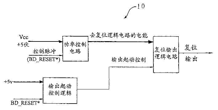
图1是按本发明功率控制电路的方框图;Fig. 1 is a block diagram by the power control circuit of the present invention;
图2是本发明功率控制电路的详细原理图;Fig. 2 is a detailed schematic diagram of the power control circuit of the present invention;
图3是本发明功率控制电路的时序图。FIG. 3 is a timing diagram of the power control circuit of the present invention.
本发明的目的是提供ATM系统的一种带功率监控制器的时延控制电路因而可以热插入/热换出电源模块的功率控制电路。The purpose of the present invention is to provide a time delay control circuit with a power monitor controller in an ATM system, so that the power control circuit of the power module can be hot-inserted/hot-swapped out.
参看图1和图2,图中分别示出了本发明电路10的方框图和原理图。电路的主要组成部分有功率控制电路20、复位输出逻辑电路25、微处理器监视功率监控器30和输出起动控制逻辑电路40。Referring to Fig. 1 and Fig. 2, the block diagram and the principle diagram of the circuit 10 of the present invention are respectively shown in the figures. The main components of the circuit are power control circuit 20 , reset output logic circuit 25 , microprocessor monitoring power monitor 30 and output enable control logic circuit 40 .
通常,电路10用监视功率监控器30的板复位(BD_RESET*)输出信号来控制功率控制电路20。如图3的时序图所示,在任何上电程序期间,控制脉冲(例如板复位)起作用以控制功率控制电路20。这反过来切断供到复位输出逻辑装置25的电,迫使复位输出端处于高阻抗状态。正常的+5伏电在板复位控制脉冲不起作用之前达到稳定状态。输出起动控制逻辑电路40来的输出起动控制信号在正常+5伏电达到稳定状态之后但在板复位控制脉冲不起作用之前不起作用。复位输出逻辑电路处于输出停用状态时,加到复位输出逻辑电路起控制作用的功率则在控制脉冲不起作用之后导通。Typically, the circuit 10 monitors the board reset (BD_RESET * ) output signal of the power monitor 30 to control the power control circuit 20 . As shown in the timing diagram of FIG. 3 , during any power-up sequence, control pulses (eg, board reset) are activated to control the power control circuit 20 . This in turn cuts off power to the reset output logic device 25, forcing the reset output to a high impedance state. The normal +5 volt power reaches a steady state before the board reset control pulse fails. The output enable control signal from the output enable control logic circuit 40 is inactive after the normal +5 volts have reached steady state but before the board reset control pulse is inactive. When the reset output logic circuit is in the output disabled state, the power added to the reset output logic circuit to play a control role is turned on after the control pulse is inactive.
相反的程序是在停电时进行的。这时,控制脉冲起作用,同时复位输出逻辑电路在正常供电(+5伏)下降到+4.65伏至4.75伏以下时就截止。The reverse procedure is performed during a power outage. At this time, the control pulse is active, and the reset output logic circuit is cut off when the normal power supply (+5 volts) drops below +4.65 volts to 4.75 volts.
应该指出的是,没有给复位输出逻辑装置供电时,复位输出逻辑电路25的输出端都处于高阻抗状态。此外,复位输出逻辑电路25的输出端在输出起动控制信不起作用时也处于高阻抗状态。It should be noted that when no power is supplied to the reset output logic device, the output terminals of the reset output logic circuit 25 are all in a high impedance state. In addition, the output terminal of the reset output logic circuit 25 is also in a high-impedance state when the output activation control signal is disabled.
这种设计真正实施起来只需要板面积小于0.2平方英寸的8插脚器件再加上若干无源元件。这种装置能在+5伏额定电压下提供1.5安以上的电流。The actual implementation of this design requires only an 8-pin device with a board area of less than 0.2 square inches plus a few passive components. This device is capable of delivering over 1.5A at +5V nominal.
现在参看图2和图3更详细地说明本发明的电路。图2是功率控制电路的原理图。图3是本发明的电路在上电和省电程序过程中的相对时序图。Referring now to FIGS. 2 and 3, the circuit of the present invention will be described in more detail. Figure 2 is a schematic diagram of the power control circuit. FIG. 3 is a relative timing diagram of the circuit of the present invention during power-on and power-saving procedures.
系统加上+5伏(Vcc)电时,微处理器的监视功率监控器30将BD_RESET*=信号加到插脚7上历时1秒左右,如图3中的A点所示。BD_RESET*=信号起作用时,功率控制电路20的输出端插脚1和插脚8都不起作用(开路)。When +5 volts (Vcc) is applied to the system, the supervisory power monitor 30 of the microprocessor applies the BD_RESET * = signal to pin 7 for about 1 second, as shown at point A in FIG. 3 . BD_RESET * = When the signal is active, both pin 1 and pin 8 of the output of the power control circuit 20 are inactive (open circuit).
BD_RESET*=信号还加到输出起动控制逻辑电路40的输入端,从而使输出起动控制信号加到复位输出逻辑装置25的输入端。+5伏电源达到稳定状态时,输出起动控制信号就停止作用(见图3的B点)。输出起动控制信号在板珍断完毕后在进一步控制过程中仍然不起作用。The BD_RESET * = signal is also applied to the input of the output enable control logic 40 so that the output enable control signal is applied to the input of the reset output logic 25 . When the +5 volt power supply reaches a steady state, the output start control signal stops functioning (see point B in Figure 3). The output start control signal still has no effect in the further control process after the board is cut off.
给监视功率监控器供电的同一个+5伏(Vcc)电压也加到功率控制电路20的插脚2上。Vcc有时在BD_RESET*信号起作用的1秒时间内稳定下来(达+5伏)。1秒钟过后,监视功率监控器30就会停止发送原先发送给功率控制电路20的BD_RESET*信号(见图3中的C点)。这时,功率控制电路20会将出现在输入端插脚2的Vcc电压转接到输出端插脚1和8上(见图3中的D点)。不应忘记,复位输出逻辑电路25的输出端会处于高阻抗状态,因为作为上电程序的一部分,输出起动控制信号因监视功率监控器30来的BD_RESET*信号而停止作用。这样,这个电路使复位线路即使监控制板上电也保持正常运行。The same +5 volt (Vcc) voltage that powers the supervisory power monitor is also applied to pin 2 of the power control circuit 20 . Vcc sometimes stabilizes (up to +5 volts) within 1 second of the BD_RESET * signal being active. After 1 second, the monitoring power monitor 30 will stop sending the BD_RESET * signal originally sent to the power control circuit 20 (see point C in FIG. 3 ). At this time, the power control circuit 20 will transfer the Vcc voltage appearing on the pin 2 of the input terminal to the pins 1 and 8 of the output terminal (see point D in FIG. 3 ). It should not be forgotten that the output of the reset output logic circuit 25 will be in a high impedance state because the output enable control signal is deactivated by monitoring the BD_RESET * signal from the power monitor 30 as part of the power up sequence. Thus, this circuit keeps the reset line functioning normally even when the supervisory board is powered on.
概括起来讲,如图3中所示,在上电程序过程中,来自监视功率监控器30的BD_RESET*控制脉冲会起作用(A点;逻辑低态)从而切断了给复位输出逻辑电路25的供电。BD_RESET*控制脉冲随着+5伏电压达到稳态而停止作用时(C点;逻辑低态),给复位输出逻辑电路25供电的通路接通(D点)。正常供电降到+4.65伏至+4.75伏以下时,给复位输出逻辑电路25的供电通路断开(E点)。In summary, as shown in FIG. 3, during the power-up sequence, the BD_RESET * control pulse from the monitoring power monitor 30 will be active (point A; logic low state) thereby cutting off the power supply to the reset output logic circuit 25. powered by. When the BD_RESET * control pulse ceases to function as the +5V voltage reaches a steady state (point C; logic low state), the path for powering the reset output logic circuit 25 is turned on (point D). When the normal power supply drops below +4.65 volts to +4.75 volts, the power supply path to the reset output logic circuit 25 is disconnected (point E).
这种设计有这样的好处。首先,无需特殊设计就可以热换出SPU后板(电源)。其次,设计包括所有固态元件,无需精确定时电路。另外,要达到这些功能只要小小的开支和面积不大的电路板即可。如果静电放电也作相应的处理,则这种设计还可以修改得使其可以隔离正常集成电路上的漏泄通路。This design has such benefits. First, the SPU backplane (power supply) can be hot-swapped without special design. Second, the design includes all solid-state components, eliminating the need for precise timing circuits. In addition, to achieve these functions, only a small expenditure and a small circuit board can be used. This design can also be modified to isolate leakage paths on normal integrated circuits if electrostatic discharge is handled accordingly.
虽然上面是就上述一些实施例说明本发明的,但本技术领域的行家们都知道,在不脱离所附权利要求书及其等效文件的精神实质和范围的前提下,是可以对本发明进行修改的。Although the present invention has been described above with respect to some of the above-mentioned embodiments, those skilled in the art know that the present invention can be carried out without departing from the spirit and scope of the appended claims and their equivalent documents. Modified.
Claims (7)
Applications Claiming Priority (2)
| Application Number | Priority Date | Filing Date | Title |
|---|---|---|---|
| US763108 | 1996-12-10 | ||
| US08/763,108 US5866958A (en) | 1996-12-10 | 1996-12-10 | Power control device for redundant reset outputs in an ATM system and method of power control thereof |
Publications (2)
| Publication Number | Publication Date |
|---|---|
| CN1195243A CN1195243A (en) | 1998-10-07 |
| CN1112005C true CN1112005C (en) | 2003-06-18 |
Family
ID=25066903
Family Applications (1)
| Application Number | Title | Priority Date | Filing Date |
|---|---|---|---|
| CN97122925A Expired - Fee Related CN1112005C (en) | 1996-12-10 | 1997-11-20 | Power Control device for redundant reset outputs in ATM system and method of power control thereof |
Country Status (5)
| Country | Link |
|---|---|
| US (1) | US5866958A (en) |
| JP (1) | JPH10210100A (en) |
| KR (1) | KR100251718B1 (en) |
| CN (1) | CN1112005C (en) |
| GB (1) | GB2320379B (en) |
Families Citing this family (4)
| Publication number | Priority date | Publication date | Assignee | Title |
|---|---|---|---|---|
| US6243782B1 (en) * | 1998-12-31 | 2001-06-05 | Intel Corporation | Method and apparatus for disabling a graphics device when an upgrade device is installed |
| US6768222B1 (en) * | 2000-07-11 | 2004-07-27 | Advanced Micro Devices, Inc. | System and method for delaying power supply power-up |
| RU2446309C2 (en) * | 2010-03-22 | 2012-03-27 | Федеральное Государственное Образовательное Учреждение Высшего Профессионального Образования "Южный Федеральный Университет" | Engine ignition system |
| RU2552105C1 (en) * | 2014-01-31 | 2015-06-10 | Федеральное государственное автономное образовательное учреждение высшего профессионального образования "Южный федеральный университет" (Южный федеральный университет) | Engine ignition system |
Family Cites Families (4)
| Publication number | Priority date | Publication date | Assignee | Title |
|---|---|---|---|---|
| US5530302A (en) * | 1994-01-13 | 1996-06-25 | Network Systems Corporation | Circuit module with hot-swap control circuitry |
| US5579491A (en) * | 1994-07-07 | 1996-11-26 | Dell U.S.A., L.P. | Local proactive hot swap request/acknowledge system |
| US5613130A (en) * | 1994-11-10 | 1997-03-18 | Vadem Corporation | Card voltage switching and protection |
| US5604873A (en) * | 1994-12-28 | 1997-02-18 | Intel Corporation | Circuitry for controlling power application to a hot docking SCSI SCA disk drive |
-
1996
- 1996-12-10 US US08/763,108 patent/US5866958A/en not_active Expired - Fee Related
-
1997
- 1997-11-18 GB GB9724308A patent/GB2320379B/en not_active Expired - Fee Related
- 1997-11-20 CN CN97122925A patent/CN1112005C/en not_active Expired - Fee Related
- 1997-12-10 JP JP9340144A patent/JPH10210100A/en active Pending
- 1997-12-10 KR KR1019970067486A patent/KR100251718B1/en not_active Expired - Fee Related
Also Published As
| Publication number | Publication date |
|---|---|
| KR19980064005A (en) | 1998-10-07 |
| US5866958A (en) | 1999-02-02 |
| GB2320379B (en) | 1999-02-24 |
| KR100251718B1 (en) | 2000-04-15 |
| GB2320379A (en) | 1998-06-17 |
| GB9724308D0 (en) | 1998-01-14 |
| JPH10210100A (en) | 1998-08-07 |
| CN1195243A (en) | 1998-10-07 |
Similar Documents
| Publication | Publication Date | Title |
|---|---|---|
| US4663539A (en) | Local power switching control subsystem | |
| US4677566A (en) | Power control network for multiple digital modules | |
| US6952785B1 (en) | Methods and apparatus for powering a data communications port | |
| EP0373773B1 (en) | Disengaging electrical circuit boards from power-supply units | |
| JP2540432B2 (en) | Module online replacement method | |
| US4635195A (en) | Power control network using reliable communications protocol | |
| JPH04232521A (en) | Common power controlling apparatus | |
| US5983298A (en) | Industrial controller permitting removal and insertion of circuit cards while under power | |
| JPH02125314A (en) | Circuit devices, circuit networks, and live wire insertion and removal methods of circuit devices | |
| JPH11305879A (en) | Interlocking control method between host, disk array and UPS | |
| CN1112005C (en) | Power Control device for redundant reset outputs in ATM system and method of power control thereof | |
| US5831346A (en) | Method and apparatus for control of power supply coupling on computer backplane | |
| JP4459408B2 (en) | Hot swap bus | |
| JP2000163164A (en) | Power source controller and no-break power unit | |
| JP2856633B2 (en) | Redundant device | |
| EP1713006A1 (en) | Methods and apparatus for managing signals during power-up and power down | |
| JPH0744293A (en) | Bus interface device | |
| JPH08256191A (en) | Data processing device | |
| KR20000044361A (en) | Clock supply control circuit of duplication board | |
| KR19990059294A (en) | Redundant switching system at the exchange | |
| JPH07253834A (en) | Module insertion / extraction control device | |
| JPH04195410A (en) | Device connection disconnection control device | |
| JP2878151B2 (en) | Parallel redundant power supply with online repair function | |
| JP3475542B2 (en) | Power supply system | |
| JPH05197448A (en) | Mother board for non-stop type computer |
Legal Events
| Date | Code | Title | Description |
|---|---|---|---|
| C10 | Entry into substantive examination | ||
| SE01 | Entry into force of request for substantive examination | ||
| C06 | Publication | ||
| PB01 | Publication | ||
| C14 | Grant of patent or utility model | ||
| GR01 | Patent grant | ||
| C19 | Lapse of patent right due to non-payment of the annual fee | ||
| CF01 | Termination of patent right due to non-payment of annual fee |