CN111490102A - Trench gate semiconductor device and method of making the same - Google Patents
Trench gate semiconductor device and method of making the same Download PDFInfo
- Publication number
- CN111490102A CN111490102A CN202010070548.9A CN202010070548A CN111490102A CN 111490102 A CN111490102 A CN 111490102A CN 202010070548 A CN202010070548 A CN 202010070548A CN 111490102 A CN111490102 A CN 111490102A
- Authority
- CN
- China
- Prior art keywords
- trench
- region
- source
- gate
- semiconductor layer
- Prior art date
- Legal status (The legal status is an assumption and is not a legal conclusion. Google has not performed a legal analysis and makes no representation as to the accuracy of the status listed.)
- Granted
Links
Images


Classifications
-
- H—ELECTRICITY
- H10—SEMICONDUCTOR DEVICES; ELECTRIC SOLID-STATE DEVICES NOT OTHERWISE PROVIDED FOR
- H10D—INORGANIC ELECTRIC SEMICONDUCTOR DEVICES
- H10D62/00—Semiconductor bodies, or regions thereof, of devices having potential barriers
- H10D62/10—Shapes, relative sizes or dispositions of the regions of the semiconductor bodies; Shapes of the semiconductor bodies
- H10D62/13—Semiconductor regions connected to electrodes carrying current to be rectified, amplified or switched, e.g. source or drain regions
- H10D62/149—Source or drain regions of field-effect devices
- H10D62/151—Source or drain regions of field-effect devices of IGFETs
- H10D62/152—Source regions of DMOS transistors
- H10D62/155—Shapes
-
- H—ELECTRICITY
- H10—SEMICONDUCTOR DEVICES; ELECTRIC SOLID-STATE DEVICES NOT OTHERWISE PROVIDED FOR
- H10D—INORGANIC ELECTRIC SEMICONDUCTOR DEVICES
- H10D30/00—Field-effect transistors [FET]
- H10D30/60—Insulated-gate field-effect transistors [IGFET]
- H10D30/63—Vertical IGFETs
-
- H—ELECTRICITY
- H10—SEMICONDUCTOR DEVICES; ELECTRIC SOLID-STATE DEVICES NOT OTHERWISE PROVIDED FOR
- H10D—INORGANIC ELECTRIC SEMICONDUCTOR DEVICES
- H10D30/00—Field-effect transistors [FET]
- H10D30/01—Manufacture or treatment
- H10D30/021—Manufacture or treatment of FETs having insulated gates [IGFET]
- H10D30/025—Manufacture or treatment of FETs having insulated gates [IGFET] of vertical IGFETs
-
- H—ELECTRICITY
- H10—SEMICONDUCTOR DEVICES; ELECTRIC SOLID-STATE DEVICES NOT OTHERWISE PROVIDED FOR
- H10D—INORGANIC ELECTRIC SEMICONDUCTOR DEVICES
- H10D30/00—Field-effect transistors [FET]
- H10D30/01—Manufacture or treatment
- H10D30/021—Manufacture or treatment of FETs having insulated gates [IGFET]
- H10D30/028—Manufacture or treatment of FETs having insulated gates [IGFET] of double-diffused metal oxide semiconductor [DMOS] FETs
- H10D30/0291—Manufacture or treatment of FETs having insulated gates [IGFET] of double-diffused metal oxide semiconductor [DMOS] FETs of vertical DMOS [VDMOS] FETs
- H10D30/0295—Manufacture or treatment of FETs having insulated gates [IGFET] of double-diffused metal oxide semiconductor [DMOS] FETs of vertical DMOS [VDMOS] FETs using recessing of the source electrodes
-
- H—ELECTRICITY
- H10—SEMICONDUCTOR DEVICES; ELECTRIC SOLID-STATE DEVICES NOT OTHERWISE PROVIDED FOR
- H10D—INORGANIC ELECTRIC SEMICONDUCTOR DEVICES
- H10D30/00—Field-effect transistors [FET]
- H10D30/01—Manufacture or treatment
- H10D30/021—Manufacture or treatment of FETs having insulated gates [IGFET]
- H10D30/028—Manufacture or treatment of FETs having insulated gates [IGFET] of double-diffused metal oxide semiconductor [DMOS] FETs
- H10D30/0291—Manufacture or treatment of FETs having insulated gates [IGFET] of double-diffused metal oxide semiconductor [DMOS] FETs of vertical DMOS [VDMOS] FETs
- H10D30/0297—Manufacture or treatment of FETs having insulated gates [IGFET] of double-diffused metal oxide semiconductor [DMOS] FETs of vertical DMOS [VDMOS] FETs using recessing of the gate electrodes, e.g. to form trench gate electrodes
-
- H—ELECTRICITY
- H10—SEMICONDUCTOR DEVICES; ELECTRIC SOLID-STATE DEVICES NOT OTHERWISE PROVIDED FOR
- H10D—INORGANIC ELECTRIC SEMICONDUCTOR DEVICES
- H10D30/00—Field-effect transistors [FET]
- H10D30/60—Insulated-gate field-effect transistors [IGFET]
- H10D30/64—Double-diffused metal-oxide semiconductor [DMOS] FETs
- H10D30/66—Vertical DMOS [VDMOS] FETs
- H10D30/668—Vertical DMOS [VDMOS] FETs having trench gate electrodes, e.g. UMOS transistors
-
- H—ELECTRICITY
- H10—SEMICONDUCTOR DEVICES; ELECTRIC SOLID-STATE DEVICES NOT OTHERWISE PROVIDED FOR
- H10D—INORGANIC ELECTRIC SEMICONDUCTOR DEVICES
- H10D62/00—Semiconductor bodies, or regions thereof, of devices having potential barriers
- H10D62/10—Shapes, relative sizes or dispositions of the regions of the semiconductor bodies; Shapes of the semiconductor bodies
- H10D62/124—Shapes, relative sizes or dispositions of the regions of semiconductor bodies or of junctions between the regions
-
- H—ELECTRICITY
- H10—SEMICONDUCTOR DEVICES; ELECTRIC SOLID-STATE DEVICES NOT OTHERWISE PROVIDED FOR
- H10D—INORGANIC ELECTRIC SEMICONDUCTOR DEVICES
- H10D62/00—Semiconductor bodies, or regions thereof, of devices having potential barriers
- H10D62/10—Shapes, relative sizes or dispositions of the regions of the semiconductor bodies; Shapes of the semiconductor bodies
- H10D62/13—Semiconductor regions connected to electrodes carrying current to be rectified, amplified or switched, e.g. source or drain regions
- H10D62/149—Source or drain regions of field-effect devices
- H10D62/151—Source or drain regions of field-effect devices of IGFETs
-
- H—ELECTRICITY
- H10—SEMICONDUCTOR DEVICES; ELECTRIC SOLID-STATE DEVICES NOT OTHERWISE PROVIDED FOR
- H10D—INORGANIC ELECTRIC SEMICONDUCTOR DEVICES
- H10D64/00—Electrodes of devices having potential barriers
- H10D64/20—Electrodes characterised by their shapes, relative sizes or dispositions
- H10D64/23—Electrodes carrying the current to be rectified, amplified, oscillated or switched, e.g. sources, drains, anodes or cathodes
- H10D64/251—Source or drain electrodes for field-effect devices
- H10D64/252—Source or drain electrodes for field-effect devices for vertical or pseudo-vertical devices
-
- H—ELECTRICITY
- H10—SEMICONDUCTOR DEVICES; ELECTRIC SOLID-STATE DEVICES NOT OTHERWISE PROVIDED FOR
- H10D—INORGANIC ELECTRIC SEMICONDUCTOR DEVICES
- H10D64/00—Electrodes of devices having potential barriers
- H10D64/20—Electrodes characterised by their shapes, relative sizes or dispositions
- H10D64/23—Electrodes carrying the current to be rectified, amplified, oscillated or switched, e.g. sources, drains, anodes or cathodes
- H10D64/251—Source or drain electrodes for field-effect devices
- H10D64/252—Source or drain electrodes for field-effect devices for vertical or pseudo-vertical devices
- H10D64/2527—Source or drain electrodes for field-effect devices for vertical or pseudo-vertical devices for vertical devices wherein the source or drain electrodes are recessed in semiconductor bodies
-
- H—ELECTRICITY
- H10—SEMICONDUCTOR DEVICES; ELECTRIC SOLID-STATE DEVICES NOT OTHERWISE PROVIDED FOR
- H10D—INORGANIC ELECTRIC SEMICONDUCTOR DEVICES
- H10D64/00—Electrodes of devices having potential barriers
- H10D64/20—Electrodes characterised by their shapes, relative sizes or dispositions
- H10D64/23—Electrodes carrying the current to be rectified, amplified, oscillated or switched, e.g. sources, drains, anodes or cathodes
- H10D64/251—Source or drain electrodes for field-effect devices
- H10D64/258—Source or drain electrodes for field-effect devices characterised by the relative positions of the source or drain electrodes with respect to the gate electrode
-
- H—ELECTRICITY
- H10—SEMICONDUCTOR DEVICES; ELECTRIC SOLID-STATE DEVICES NOT OTHERWISE PROVIDED FOR
- H10D—INORGANIC ELECTRIC SEMICONDUCTOR DEVICES
- H10D64/00—Electrodes of devices having potential barriers
- H10D64/20—Electrodes characterised by their shapes, relative sizes or dispositions
- H10D64/27—Electrodes not carrying the current to be rectified, amplified, oscillated or switched, e.g. gates
- H10D64/311—Gate electrodes for field-effect devices
- H10D64/411—Gate electrodes for field-effect devices for FETs
- H10D64/511—Gate electrodes for field-effect devices for FETs for IGFETs
- H10D64/512—Disposition of the gate electrodes, e.g. buried gates
- H10D64/513—Disposition of the gate electrodes, e.g. buried gates within recesses in the substrate, e.g. trench gates, groove gates or buried gates
-
- H—ELECTRICITY
- H10—SEMICONDUCTOR DEVICES; ELECTRIC SOLID-STATE DEVICES NOT OTHERWISE PROVIDED FOR
- H10D—INORGANIC ELECTRIC SEMICONDUCTOR DEVICES
- H10D64/00—Electrodes of devices having potential barriers
- H10D64/20—Electrodes characterised by their shapes, relative sizes or dispositions
- H10D64/27—Electrodes not carrying the current to be rectified, amplified, oscillated or switched, e.g. gates
- H10D64/311—Gate electrodes for field-effect devices
- H10D64/411—Gate electrodes for field-effect devices for FETs
- H10D64/511—Gate electrodes for field-effect devices for FETs for IGFETs
- H10D64/514—Gate electrodes for field-effect devices for FETs for IGFETs characterised by the insulating layers
- H10D64/516—Gate electrodes for field-effect devices for FETs for IGFETs characterised by the insulating layers the thicknesses being non-uniform
Landscapes
- Electrodes Of Semiconductors (AREA)
Abstract
本公开涉及一种功率半导体装置及其制造方法,该功率半导体装置包括:半导体层,其限定第一主表面并且包括漂移区;沟槽,其从第一主表面延伸至半导体层中,其中,沟槽包括由栅极电介质包围的栅电极,该栅极电介质被构造和布置为将栅电极与半导体层电隔离;以及源极区,其从第一主表面延伸,并且与沟槽的顶部侧壁部分邻接,其中,源极区延伸至与栅电极的顶表面对应的深度。
The present disclosure relates to a power semiconductor device and a method of fabricating the same, the power semiconductor device comprising: a semiconductor layer defining a first main surface and including a drift region; a trench extending from the first main surface into the semiconductor layer, wherein, The trench includes a gate electrode surrounded by a gate dielectric constructed and arranged to electrically isolate the gate electrode from the semiconductor layer; and a source region extending from the first major surface and connected to a top side of the trench The wall portion adjoins, wherein the source region extends to a depth corresponding to the top surface of the gate electrode.
Description
技术领域technical field
本公开涉及一种半导体装置。具体地说,本公开涉及一种分立的沟槽栅极MOSFET半导体装置和相关的制造方法。The present disclosure relates to a semiconductor device. In particular, the present disclosure relates to a discrete trench gate MOSFET semiconductor device and associated method of fabrication.
背景技术Background technique
沟槽栅极半导体装置通常包括朝向装置的第一主表面的源极区和形成在与第一主表面相对的第二主表面上的漏极区。源极区和漏极区具有相同的导电类型。在源极和漏极之间布置有主体区,主体区具有与源极区和漏极区的导电类型相反的导电类型。为了导通装置,使得其在源极和漏极之间传导电流,必须生成通过主体区的沟道。为了便于生成沟道,将沟槽栅电极设置在装置内的沟槽中靠近但不接触主体区。A trench gate semiconductor device typically includes a source region facing a first major surface of the device and a drain region formed on a second major surface opposite the first major surface. The source and drain regions have the same conductivity type. A body region is arranged between the source and drain, the body region having an opposite conductivity type to that of the source and drain regions. In order to turn on the device so that it conducts current between the source and drain, a channel must be created through the body region. To facilitate channel generation, trench gate electrodes are positioned in the trenches within the device near but not touching the body region.
沟槽通常衬有氧化物,以将栅电极与主体区电隔离。在栅极处提供偏压会产生电场,该电场延伸到主体区中并局部耗尽和反转主体区。The trenches are typically lined with oxide to electrically isolate the gate electrode from the body region. Providing a bias voltage at the gate generates an electric field that extends into the body region and locally depletes and inverts the body region.
沟槽栅极半导体装置能够进行高电压(即,在100V范围内)工作。此外,这种装置还能够在源极和漏极之间提供高达250V的反向偏压,而不会使装置发生故障或使任何显著的反向电流从中通过。这可以通过在漏极区和主体区之间包括漂移区来实现,其中,漂移区具有与源极区和漏极区相同的导电类型,但是掺杂浓度较低。该漏极区在与主体区的交界处形成p-n结,阻止高反向偏压电流。对于n沟道装置,漏极相对于源极是正性的。如果源极相对于漏极是正性的,则主体-漏极结变得有偏压,并且电流经由漏极和源极传导。相反,对于p沟道装置,漏极相对于源极是负性的。如果源极相对于漏极是负性的,则主体-漏极结再次传导电流。击穿电压取决于漂移区的厚度;Trench gate semiconductor devices are capable of high voltage (ie, in the 100V range) operation. In addition, the device is capable of providing up to 250V of reverse bias between the source and drain without failing the device or passing any significant reverse current through it. This can be achieved by including a drift region between the drain and body regions, wherein the drift region has the same conductivity type as the source and drain regions, but with a lower doping concentration. The drain region forms a p-n junction at the junction with the body region, preventing high reverse bias currents. For n-channel devices, the drain is positive with respect to the source. If the source is positive with respect to the drain, the body-drain junction becomes biased and current conducts through the drain and source. Conversely, for p-channel devices, the drain is negative with respect to the source. If the source is negative with respect to the drain, the body-drain junction again conducts current. The breakdown voltage depends on the thickness of the drift region;
其中,厚度越大,击穿电压越高。Among them, the larger the thickness, the higher the breakdown voltage.
上述布置一般如图1所示,其中,沟槽栅极半导体装置包括在其第一主表面11处的源极区1和形成装置的漏极区2的衬底。主体区3和漂移区域6布置在源极区1和漏极区2之间。沟槽4从第一主表面11向下延伸,穿过源极区1和主体区3,并终止于漂移区6。沟槽4的侧壁和底部衬有绝缘材料5,以物理地并电气地将位于沟槽4内的栅极8与周围区隔离。通过源极区10形成沟9,其终止于主体区3以便允许在源极区10与主体区3之间形成低电阻欧姆电触点。The above arrangement is generally shown in Figure 1, wherein a trench gate semiconductor device includes a
与传统的横向MOSFET装置(如横向DMOS)相比,在纵向沟槽栅极半导体装置(如上述类型)中,沟道区是沿着沟槽的竖直壁而不是横向进行设计的,因此允许每单位装置面积的高沟道密度(每沟槽两个沟道)。然而,沟槽密度增大的限制因素是占据装置面积的沟9区的宽度,并确保沟9至沟槽栅极8的距离大于沟9与沟槽栅极8之间的对齐处理的公差。因此,沟区的宽度和对齐处理的公差限制了每装置单位面积的沟槽单元的最大数量。In contrast to conventional lateral MOSFET devices (such as lateral DMOS), in vertical trench gate semiconductor devices (such as the type described above), the channel region is designed along the vertical walls of the trench rather than laterally, thus allowing High channel density per unit device area (two channels per trench). However, the limiting factor for increased trench density is the width of the
发明内容SUMMARY OF THE INVENTION
各示例实施例是针对诸如上文所述的问题和/或其他问题的,这些问题可从以下公开中变得明显,例如关于提高沟槽栅极半导体装置的每单位面积的沟道密度。Example embodiments are directed to problems such as those described above and/or other problems, which may become apparent from the following disclosure, eg, with respect to increasing the channel density per unit area of trench gate semiconductor devices.
在特定示例实施例中,本公开的各方面涉及一种源极触点,其形成在栅极上方,因此允许去除传统的用于接触源极区和主体区的沟区构造。此外,布置在栅极电介质的顶表面上并且电连接源极区与主体区的源极触点还允许源极区与栅电极对齐。In certain example embodiments, aspects of the present disclosure relate to a source contact formed over a gate, thus allowing the removal of conventional trench configuration for contacting source and body regions. In addition, the source contact disposed on the top surface of the gate dielectric and electrically connecting the source region and the body region also allows the source region to align with the gate electrode.
根据实施例,提供了一种分立的功率半导体装置,其包括:半导体层,其限定第一主表面并且包括漂移区;沟槽,其从第一主表面延伸至半导体层中,其中,沟槽包括由栅极电介质包围的栅电极,该栅极电介质被构造和布置为使栅电极与半导体层电隔离;以及源极区,其从第一主表面延伸,并且与沟槽的顶部侧壁部分邻接,其中,源极区延伸至与栅电极的顶表面对应的深度。According to an embodiment, there is provided a discrete power semiconductor device comprising: a semiconductor layer defining a first main surface and including a drift region; a trench extending from the first main surface into the semiconductor layer, wherein the trench including a gate electrode surrounded by a gate dielectric constructed and arranged to electrically isolate the gate electrode from the semiconductor layer; and a source region extending from the first major surface and being separated from a top sidewall portion of the trench Adjacent, wherein the source region extends to a depth corresponding to the top surface of the gate electrode.
半导体装置还可包括从第一主表面延伸至半导体层中的主体区;其中,主体区在其上部与源极区邻接,并且在其下部与沟槽邻接。The semiconductor device may further include a body region extending from the first major surface into the semiconductor layer; wherein the body region adjoins the source region at an upper portion thereof and abuts the trench at a lower portion thereof.
源极触点可电连接至源极区和主体区,并且/或源极触点可被构造和布置在栅极电介质的上部上。A source contact may be electrically connected to the source and body regions, and/or the source contact may be constructed and arranged on an upper portion of the gate dielectric.
主体区可在与源极区的与沟槽邻接的一侧相对的一侧上与源极区邻接。The body region may adjoin the source region on a side opposite the side of the source region adjoining the trench.
半导体装置还可包括半导体衬底,其中,半导体层被构造和布置在半导体衬底上,并且沟槽可延伸至半导体层的漂移区中并且在漂移区中终止。The semiconductor device may also include a semiconductor substrate, wherein a semiconductor layer is constructed and arranged on the semiconductor substrate, and the trenches may extend into and terminate in a drift region of the semiconductor layer.
根据实施例,还提供了一种制造功率半导体装置的方法,所述方法包括:形成限定第一主表面并且包括漂移层的半导体层;形成从第一主表面延伸至半导体层中的沟槽;形成由栅极电介质包围的栅电极,该栅极电介质被构造和布置为将栅电极与半导体层电隔离;以及形成从第一主表面延伸并且与沟槽的顶部侧壁部分邻接的源极区,其中,源极区延伸至与栅电极的顶表面对应的深度。According to an embodiment, there is also provided a method of fabricating a power semiconductor device, the method comprising: forming a semiconductor layer defining a first main surface and including a drift layer; forming a trench extending into the semiconductor layer from the first main surface; forming a gate electrode surrounded by a gate dielectric constructed and arranged to electrically isolate the gate electrode from the semiconductor layer; and forming a source region extending from the first major surface and adjoining a top sidewall portion of the trench , wherein the source region extends to a depth corresponding to the top surface of the gate electrode.
制造半导体装置的方法还可包括:形成从第一主表面延伸至半导体层中的主体区;其中,主体区被形成为在其上部与源极区邻接,并且在其下部与沟槽邻接。The method of fabricating a semiconductor device may further include forming a body region extending from the first main surface into the semiconductor layer; wherein the body region is formed to adjoin the source region at an upper portion thereof and abut the trench at a lower portion thereof.
所述方法还可包括:形成电连接至源极区和主体区的源极触点,并且在栅极电介质的上部上形成源极触点。The method may further include forming a source contact electrically connected to the source region and the body region, and forming the source contact on an upper portion of the gate dielectric.
主体区可被形成为在源极区的与沟槽邻接的一侧相对的一侧上与源极区邻接。半导体层可形成在半导体衬底上,并且沟槽可形成为延伸至半导体层的漂移区中,并且在漂移区中终止。The body region may be formed adjoining the source region on a side of the source region opposite the side adjoining the trench. A semiconductor layer may be formed on a semiconductor substrate, and a trench may be formed extending into and terminating in a drift region of the semiconductor layer.
结果,技术人员应该认识到,根据上述实施例的沟槽半导体装置的布置和对应的制造方法可实现每单位面积更高密度的有源单元。As a result, skilled artisans will appreciate that the arrangement of trench semiconductor devices and corresponding fabrication methods according to the above-described embodiments can achieve a higher density of active cells per unit area.
附图说明Description of drawings
因此,按照其中可详细理解本公开的特征的方式,参照实施例进行更具体的描述,一些实施例在附图中示出。然而,应该注意,附图仅示出了典型实施例,因此不应理解为对其范围的限制。附图用于便于理解本公开,因此不一定按照比例绘制。本领域技术人员一旦结合附图阅读了本说明书就将清楚要求保护的主题内容的优点,图中相同参考标号用于指代相同元件,其中:Thus, in the manner in which the features of the present disclosure may be understood in detail, a more specific description will be made with reference to embodiments, some of which are illustrated in the accompanying drawings. It is to be noted, however, that the appended drawings illustrate only typical embodiments and are therefore not to be considered limiting of their scope. The drawings are used to facilitate an understanding of the present disclosure and are therefore not necessarily drawn to scale. The advantages of the claimed subject matter will become apparent to those skilled in the art upon reading this specification in conjunction with the accompanying drawings, wherein like reference numerals are used to refer to like elements, wherein:
图1示出了已知的沟槽栅极半导体装置的一部分的剖面图;1 shows a cross-sectional view of a portion of a known trench gate semiconductor device;
图2a至图2l示出了制造根据实施例的沟槽栅极半导体装置的各种处理步骤;以及Figures 2a-2l illustrate various process steps for fabricating a trench gate semiconductor device according to an embodiment; and
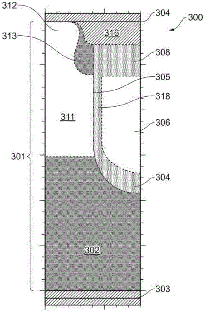
图3示出了根据实施例的沟槽栅极半导体装置的一部分。3 illustrates a portion of a trench gate semiconductor device according to an embodiment.
具体实施方式Detailed ways
根据图2a至图2l所示的处理步骤制造根据实施例的沟槽栅极半导体装置。在图2a的处理之前,可利用诸如外延生长或沉积的已知技术在半导体衬底(未示出)上形成半导体层。通常,半导体层由硅形成,并且由与半导体衬底相同的导电类型形成,例如n型。在形成限定沟槽栅极半导体装置的漂移区202的半导体层之后,穿过形成漂移区202的半导体层的顶部主表面形成栅极沟槽204,如图2a所示。可通过任何合适的蚀刻技术形成稍后将限定装置的栅极的栅极沟槽204,以使得其在漂移区202中终止,也就是说,其不延伸至半导体衬底中。栅极沟槽204包括底部和相对的侧壁。A trench gate semiconductor device according to an embodiment is fabricated according to the processing steps shown in FIGS. 2a-2l. Prior to the processing of Figure 2a, a semiconductor layer may be formed on a semiconductor substrate (not shown) using known techniques such as epitaxial growth or deposition. Typically, the semiconductor layer is formed of silicon, and is formed of the same conductivity type as the semiconductor substrate, eg, n-type. After forming the semiconductor layer defining the
在形成栅极沟槽204之后,氧化层206(已知为厚底氧化物(TBO)206)形成在栅极沟槽204的底部。例如,TBO 206可通过硅的局部氧化(LOCOS)形成。类似地,栅极沟槽204的侧壁衬有侧壁氧化物208。侧壁氧化物208可延伸以覆盖形成漂移区202的半导体层的顶部主表面。在形成侧壁氧化物208和厚底氧化物206之后,在栅极沟槽204中形成栅电极210。After the
可通过合适的工艺(诸如多晶硅的沉积)形成栅电极210。厚底氧化物206和侧壁氧化物208共同形成被构造和被布置为将栅电极210与周围的漂移区202以及任何随后形成的半导体区电绝缘的栅极氧化物(第一氧化层),如下面更详细的讨论。The
现在转到图2b,通过使用栅极电介质氧化层212(第二氧化层)Turning now to Figure 2b, by using gate dielectric oxide 212 (second oxide)
(例如,可为正硅酸乙酯(TEOS)层,然而,本领域技术人员将理解,可使用任何合适的氧化物电介质)进行沉积并覆盖栅电极210来继续进行处理。随后将栅极电介质氧化层212平面化,以使其顶表面与形成漂移区202的半导体层的顶部主表面实质上齐平。平面化的这个步骤也可去除形成在漂移区202的顶部主表面上的任何侧壁氧化物208。可通过任何合适的处理(诸如化学机械抛光(CMP))来实现平面化。栅极电介质氧化层212的平面化提供了平坦的表面,以实现栅极电介质的顶部平面性。(For example, a layer of tetraethyl orthosilicate (TEOS) may be used, however, those skilled in the art will understand that any suitable oxide dielectric may be used) to deposit and cover the
在平面化处理之后,并且如图2c所示,屏蔽(screen)氧化层214(第三氧化层)形成在氧化层212和半导体层的顶部主表面上。屏蔽氧化层214可为热生长层、TEOS或任何其它合适的氧化物电介质。屏蔽氧化层214用作注入垫氧化物,它的设置是为了将主体形成期间的高能注入损伤最小化,如下面的讨论。这种注入损伤可导致在半导体层的顶部主表面的不期望的位错。After the planarization process, and as shown in Figure 2c, a screen oxide layer 214 (third oxide layer) is formed on the
在将要去除屏蔽氧化物的源极注入部分之前,将栅极沟槽中的屏蔽氧化层214回蚀。可选地,可在源极注入之前形成额外的屏蔽氧化层(未示出)。The
然后,在如图2d所示的半导体层中形成沟槽栅极半导体装置的主体区211。例如,可通过利用硼注入将p型物质注入(n型)漂移区202中来实现主体区211的形成。主体区211延伸至与栅极沟槽204的侧壁对应的深度。如上所述,形成主体区211使得在操作期间,穿过邻近于栅电极210的主体区生成沟道区。如上所述,屏蔽氧化层214防止在形成主体区211期间发生注入损伤。Then, the
如图2e所示,在形成主体区211之后,通过从半导体层的顶表面和栅极沟槽204进行蚀刻,来去除屏蔽氧化层214。另外,例如通过从栅极沟槽204进行蚀刻,来部分地去除栅极电介质氧化层212。此外,从栅极沟槽204的侧壁部分地去除侧壁氧化物208,留下覆盖栅电极210的一层栅极电介质氧化层212。这样,暴露出栅极沟槽204的侧壁,用于以后形成源极区213,如下面的讨论。As shown in FIG. 2e, after the
栅电极210上方的剩余的栅极电介质氧化层212的厚度可为大约200nm,但这取决于源极注入物的要求深度。源极区213与栅极对齐,并且被注入与栅极沟槽的侧壁对应的半导体层中,以至少与栅电极210顶部的层面一样深。栅极电介质氧化层212被布置为限定源极注入深度的范围。如果栅极电介质氧化层212太厚,则源极将被不正确地限定,并且源极注入物将不能到达栅电极210顶部的层面。如果栅极电介质氧化层212太薄,则源极可被注入太深,导致沟道区深度较小。这样,本领域技术人员应该看到,剩余的栅极电介质氧化层212的厚度是设计变量,并且取决于注入的能量和所需的装置结构。The thickness of the remaining gate
现在参照图2f,沟槽栅极半导体装置的源极区213随后形成在与主体区211的上部对应的半导体层区中,主体区211与栅极沟槽204邻接。可通过将n型物质注入先前形成的主体区211的栅极沟槽204侧壁的上部中来实现源极区213的形成。上面针对图2e讨论了侧壁的上部通过氧化蚀刻处理暴露出来。可通过相对于半导体层的顶表面非垂直的有角度的注入来实现n型物质的注入。注入物可为任何合适的n型物质,诸如砷。所述有角度的注入允许n型物质到达栅极沟槽204的暴露的侧壁,因此形成源极区213。Referring now to FIG. 2f , the
在形成源极区213之后,氧化物插塞216(第四氧化物)形成在栅极沟槽204中,并且通过例如CMP被平面化。氧化物插塞216被构造为限定源极敷金属(metallisation)触点区(下面更详细地讨论),并且在后面的氧化物插塞216的蚀刻处理之后,将后面形成的源极注入物与氧化物插塞216对齐。这样,不需要针对源极注入物的光刻步骤,因为源极的范围由氧化物插塞216限定。如图2g所示,氧化物插塞216被沉积,并且随后被平面化,使得其中形成有源极区213的半导体层的顶部主表面暴露出来。After the
氧化物插塞216随后例如通过蚀刻从栅极沟槽204中被部分去除,即,从栅极沟槽204的侧壁被去除,留下形成在栅电极210上面的几层氧化层212和216,如图2h所示。在该步骤中,蚀刻氧化物插塞216直至到达硅层的顶部主表面下方的层面。这允许稍后去除硅层的顶部主表面的顶部部分(如下面针对图2i讨论的),使得其最终与氧化物插塞216齐平,并且去除硅的表面,并且替换为源极触点注入物(下面进行讨论)。源极触点注入物比源极区注入物的剂量小,以有效地使装置的主体区和源极区短路。必须去除硅的表面上的源极区注入物,从而形成短路。
如图2i所示,随后对半导体层的顶部主表面回蚀,以去除任何高剂量的n型物质。氧化物插塞216可用作掩模,并且提供表面以防止在形成源极触点区215期间注入物从插塞反射至硅的侧壁上。氧化物插塞216还用于通过减小注入的物质的剂量来防止源极触点区的过度掺杂。此外,掩模防止注入的物质深入地渗入到沟道区中,这可导致装置阈电压由于增加沟道区的掺杂而偏离。另外,源极触点区215注入物将不对源极区213注入物进行过量掺杂,但其将具有减小源极区的掺杂的净效果,这将增大触点电阻。As shown in Figure 2i, the top major surface of the semiconductor layer is then etched back to remove any high doses of n-type species.
在图2i的蚀刻步骤之后,源极触点区215形成在与顶部主表面处的源极区213和主体区211对应的半导体层的顶部主表面,如图2j所示。可通过将p型物质直接注入半导体层中来实现源极触点区215的形成。例如,可通过硼/氟(BF2)的注入来实现这种注入。源极区213和源极触点区215经由顶侧源极触点敷金属被电连接。这种连接仅在存在低触点电阻时有效,并且经由触点区215注入物和源极区213注入物的高剂量p型物质实现低触点电阻。After the etching step of Figure 2i, a
在图2j的源极触点区215形成之后,随后蚀刻氧化物插塞216以允许形成源极触点敷金属(下面讨论),如图2k所示。这导致到源极区213的源极触点敷金属面积足够大,以确保到其的电连接。After the
现在参照图2l,源极敷金属217随后形成在与源极区213对应的半导体层的顶部主表面上以及氧化物插塞216上。源极敷金属217可为铝或其它合适的金属,并且可通过任何合适处理的工艺形成。源极敷金属217接触半导体层的顶表面的整个顶表面,并且填充氧化物插塞216与栅极沟槽中的硅表面之间的区域。Referring now to FIG. 21 , source metallization 217 is then formed on the top major surface of the semiconductor layer corresponding to source
金属硅化物218(诸如硅化钨)可形成在半导体层的顶部主表面上,以形成与源极敷金属217的触点区域。这允许减小给定的触点区域的触点电阻。
现在转到图3,示出了根据实施例的沟槽栅极半导体装置300的有源单元区的半单元。本领域技术人员将理解,图3的布置是完整单元的一半,并且沟槽栅极半导体装置300可包括一个或多个这种单元。沟槽栅极半导体装置300可包括布置在半导体衬底303上的半导体层301。半导体层包括形成在n型半导体衬底303上的n型漂移区302,n型半导体衬底303和n型漂移区302共同地形成半导体装置300的漏极区。虽然图3中未示出,但是本领域技术人员将理解,漏极接触件可通过任何合适的手段形成在半导体衬底303上。Turning now to FIG. 3 , a half-cell of an active cell region of a trench
栅极沟槽305布置为从半导体装置300的顶部延伸至半导体层301中,并且在漂移区302中终止。TBO 304形成在栅极沟槽305的底部(或基底)中,侧壁氧化物318形成在栅极沟槽305的侧壁上,并且栅极电介质308形成在栅极沟槽305的顶部。
侧壁氧化物318、沟槽底部氧化物(TBO)304和栅极电介质308共同地形成用于将栅电极306电隔离的电介质。这样,栅电极306布置在栅极沟槽305中,并且由对应的氧化物304、308、318包围。
半导体装置300还包括p型主体区311,除了下面讨论的源极区313,p型主体区311从装置的顶部主表面延伸到与栅极沟槽305的侧壁对应的深度。换句话说,主体区311延伸至半导体装置中,并且在栅极沟槽305的底部或栅极沟槽305的底部之前终止。主体区311沿着栅极沟槽305的长度邻接栅极沟槽305,该长度从与栅电极306的顶部对应的点开始,并且如上所述在栅极沟槽305的底部或栅极沟槽305的底部之前终止。这样,主体区311在其上部与源极区313邻接并且在其下部与栅极沟槽305邻接。这允许在操作期间通过反转形成半导体装置300的源极到漏极传导通道。The
n型源极区313从半导体装置300的顶表面延伸,与源极接触区312相邻,并且沿着栅极沟槽305的长度邻接栅极沟槽305,该长度从与栅极电介质308的顶表面对应的点开始至与栅电极306的顶表面对应的点。因此,源极区313进入半导体装置300的深度对应于源极敷金属316(下文讨论)和栅极电介质308的厚度。因此,源极区313延伸到栅极沟槽305的与栅电极306的顶表面对应的深度。这种布置形成了与栅电极306的顶表面对齐的源极区313,这导致降低的动态栅极电荷(Qgs)并改善装置的开关性能,进而导致沟槽栅极半导体装置在较低温度下并且以较高效率工作。The n-
因此,源极敷金属316布置在栅极电介质308的顶表面上,并且电连接源极区313和主体区311,使得源极区313与栅电极306对齐。Accordingly, source metallization 316 is disposed on the top surface of
这样,本领域技术人员将看到,源极触点形成在半导体装置300的栅极沟槽305的上方。这允许去除用于接触源极区311和主体区313的传统的沟区构造。因此,本领域技术人员将看到,根据上述实施例的沟槽半导体装置300的布置能够实现单位面积上更高密度的有源单元。As such, those skilled in the art will appreciate that the source contact is formed over the
虽然未示出,但是本领域技术人员将理解,可以通过任何适当的手段实现与栅极多晶硅的接触。举例来说,通过刻蚀穿过栅极氧化物进入栅电极并在其中形成适当的敷金属,可仅形成栅极触点。Although not shown, those skilled in the art will understand that contact with the gate poly may be achieved by any suitable means. For example, only the gate contact may be formed by etching through the gate oxide into the gate electrode and forming a suitable metallization therein.
本领域技术人员将理解,如上所述的p型区和n型区可以并列而不偏离所述实施例的本发明构思。上述讨论涉及n沟道装置,其中,栅极是n型并且电子作为大多数载流子。然而,本领域技术人员还将理解,上述讨论对于p沟道装置也是有效的,其中,栅极是p型并且空穴作为大多数载流子。Those skilled in the art will appreciate that the p-type and n-type regions described above may be juxtaposed without departing from the inventive concept of the described embodiments. The above discussion refers to n-channel devices, where the gate is n-type and electrons are the majority carriers. However, those skilled in the art will also understand that the above discussion is also valid for p-channel devices, where the gate is p-type and holes are the majority carriers.
本发明的具体和优选方面在所附的独立权利要求中阐述。从属权利要求和/或独立权利要求中的特征的组合可适当地组合,而不仅仅如权利要求中所阐述的。Particular and preferred aspects of the invention are set out in the appended independent claims. Combinations of features in the dependent claims and/or the independent claims may be combined as appropriate and not merely as set forth in the claims.
本公开的范围包括其中明示或暗示地公开的任何新颖特征或特征组合,或其任何概括,而不论其是否与所要求保护的发明有关,或减轻本发明解决的任何或所有问题。申请人在此通知,在本申请或由此衍生的任何此类进一步申请的申请期间,可针对这些特征提出新的权利要求。具体地说,参照所附权利要求,来自从属权利要求的特征可以与独立权利要求的特征组合,并且来自各个独立权利要求的特征可以以任何适当的方式组合,而不仅仅是以权利要求中列举的特定组合。The scope of the present disclosure includes any novel feature or combination of features disclosed therein, expressly or implicitly, or any generalization thereof, whether or not related to the claimed invention or alleviating any or all problems solved by the invention. Applicants hereby notify that new claims may be made to these features during the filing of this application or any such further application derived therefrom. In particular, with reference to the appended claims, features from the dependent claims may be combined with features from the independent claims, and features from the individual independent claims may be combined in any suitable manner, not just as recited in the claims specific combination.
在各个实施例的上下文中描述的特征也可以在单个实施例中组合被提供。相反,为了简洁起见,在单个实施例的上下文中描述的各种特征也可以分别或以任何合适的子组合被提供。Features that are described in the context of various embodiments can also be provided in combination in a single embodiment. Conversely, various features that are, for brevity, described in the context of a single embodiment, may also be provided separately or in any suitable subcombination.
术语“包含”不排除其它元件或步骤,术语“一个”或“一”不排除多个。权利要求中的附图标记不得解释为限制权利要求的范围。The term "comprising" does not exclude other elements or steps, and the term "a" or "an" does not exclude a plurality. Reference signs in the claims shall not be construed as limiting the scope of the claims.
Claims (14)
Applications Claiming Priority (2)
| Application Number | Priority Date | Filing Date | Title |
|---|---|---|---|
| EP19154245.5 | 2019-01-29 | ||
| EP19154245.5A EP3690952A1 (en) | 2019-01-29 | 2019-01-29 | Trench gate semiconductor device and method of manufacture |
Publications (2)
| Publication Number | Publication Date |
|---|---|
| CN111490102A true CN111490102A (en) | 2020-08-04 |
| CN111490102B CN111490102B (en) | 2024-08-06 |
Family
ID=65243418
Family Applications (1)
| Application Number | Title | Priority Date | Filing Date |
|---|---|---|---|
| CN202010070548.9A Active CN111490102B (en) | 2019-01-29 | 2020-01-21 | Trench gate semiconductor device and method of manufacturing the same |
Country Status (3)
| Country | Link |
|---|---|
| US (1) | US11222974B2 (en) |
| EP (1) | EP3690952A1 (en) |
| CN (1) | CN111490102B (en) |
Families Citing this family (1)
| Publication number | Priority date | Publication date | Assignee | Title |
|---|---|---|---|---|
| EP4513569A1 (en) | 2023-08-24 | 2025-02-26 | Nexperia B.V. | Method of manufacturing mosfets |
Citations (5)
| Publication number | Priority date | Publication date | Assignee | Title |
|---|---|---|---|---|
| CN1536630A (en) * | 2003-04-03 | 2004-10-13 | Manufacturing method of vertical MOS transistor | |
| US20110133258A1 (en) * | 2009-08-14 | 2011-06-09 | Alpha And Omega Semiconductor Incorporated | Shielded gate trench mosfet with increased source-metal contact |
| CN103426916A (en) * | 2012-05-14 | 2013-12-04 | 飞思卡尔半导体公司 | Power MOSFET structure and method |
| CN108336141A (en) * | 2017-01-19 | 2018-07-27 | 艾普凌科有限公司 | Semiconductor device and its manufacturing method |
| CN108574002A (en) * | 2017-03-14 | 2018-09-25 | 艾普凌科有限公司 | Semiconductor device |
Family Cites Families (13)
| Publication number | Priority date | Publication date | Assignee | Title |
|---|---|---|---|---|
| JP2008546189A (en) * | 2005-05-26 | 2008-12-18 | フェアチャイルド・セミコンダクター・コーポレーション | Trench gate field effect transistor and method of manufacturing the same |
| US20080199995A1 (en) * | 2007-02-15 | 2008-08-21 | Debra Susan Woolsey | Integrated Hydrogen Anneal and Gate Oxidation for Improved Gate Oxide Integrity |
| US7956411B2 (en) * | 2008-01-15 | 2011-06-07 | Fairchild Semiconductor Corporation | High aspect ratio trench structures with void-free fill material |
| US20090272982A1 (en) * | 2008-03-03 | 2009-11-05 | Fuji Electric Device Technology Co., Ltd. | Trench gate type semiconductor device and method of producing the same |
| WO2011087994A2 (en) * | 2010-01-12 | 2011-07-21 | Maxpower Semiconductor Inc. | Devices, components and methods combining trench field plates with immobile electrostatic charge |
| WO2011133481A2 (en) * | 2010-04-20 | 2011-10-27 | Maxpower Semiconductor Inc. | Power mosfet with embedded recessed field plate and methods of fabrication |
| JP6179409B2 (en) * | 2014-01-24 | 2017-08-16 | 株式会社デンソー | Method for manufacturing silicon carbide semiconductor device |
| US12284817B2 (en) * | 2016-06-10 | 2025-04-22 | Maxpower Semiconductor Inc. | Trench-gated heterostructure and double-heterostructure active devices |
| JP6967352B2 (en) * | 2017-02-07 | 2021-11-17 | ローム株式会社 | Semiconductor devices, manufacturing methods for semiconductor devices, and semiconductor wafer structures. |
| JP2019114643A (en) * | 2017-12-22 | 2019-07-11 | ルネサスエレクトロニクス株式会社 | Semiconductor device and method for manufacturing the same |
| CN108172622A (en) * | 2018-01-30 | 2018-06-15 | 电子科技大学 | power semiconductor device |
| DE102018130385B4 (en) * | 2018-11-29 | 2024-11-14 | Infineon Technologies Ag | Silicon carbide devices and methods for forming silicon carbide devices |
| US11658241B2 (en) * | 2018-12-31 | 2023-05-23 | Texas Instruments Incorporated | Vertical trench gate MOSFET with integrated Schottky diode |
-
2019
- 2019-01-29 EP EP19154245.5A patent/EP3690952A1/en active Pending
-
2020
- 2020-01-21 CN CN202010070548.9A patent/CN111490102B/en active Active
- 2020-01-28 US US16/774,436 patent/US11222974B2/en active Active
Patent Citations (5)
| Publication number | Priority date | Publication date | Assignee | Title |
|---|---|---|---|---|
| CN1536630A (en) * | 2003-04-03 | 2004-10-13 | Manufacturing method of vertical MOS transistor | |
| US20110133258A1 (en) * | 2009-08-14 | 2011-06-09 | Alpha And Omega Semiconductor Incorporated | Shielded gate trench mosfet with increased source-metal contact |
| CN103426916A (en) * | 2012-05-14 | 2013-12-04 | 飞思卡尔半导体公司 | Power MOSFET structure and method |
| CN108336141A (en) * | 2017-01-19 | 2018-07-27 | 艾普凌科有限公司 | Semiconductor device and its manufacturing method |
| CN108574002A (en) * | 2017-03-14 | 2018-09-25 | 艾普凌科有限公司 | Semiconductor device |
Also Published As
| Publication number | Publication date |
|---|---|
| US11222974B2 (en) | 2022-01-11 |
| CN111490102B (en) | 2024-08-06 |
| EP3690952A1 (en) | 2020-08-05 |
| US20200243679A1 (en) | 2020-07-30 |
Similar Documents
| Publication | Publication Date | Title |
|---|---|---|
| US11664434B2 (en) | Semiconductor power devices having multiple gate trenches and methods of forming such devices | |
| CN203659875U (en) | Semiconductor device | |
| CN102856182B (en) | Manufacture method and the structure of Iusulated gate semiconductor device | |
| CN101290936B (en) | Semiconductor device and method for manufactruing of the same | |
| CN101764159B (en) | Metal Oxide Semiconductor Field Effect Transistor Devices with Reduced Breakdown Voltage | |
| US7868394B2 (en) | Metal-oxide-semiconductor transistor and method of manufacturing the same | |
| KR100967883B1 (en) | Trench DMOS devices with improved drain contacts | |
| CN101740515B (en) | Semiconductor element and manufacturing method | |
| US9627526B2 (en) | Assymetric poly gate for optimum termination design in trench power MOSFETs | |
| CN110459604A (en) | Shielded Trench Devices | |
| CN105280714A (en) | Insulated gate semiconductor device having a shield electrode structure and method | |
| CN101645448A (en) | Rectifier with pn clamp regions under trenches | |
| TW202006956A (en) | Power MOSFET with an integrated pseudo-Schottky diode in source contact trench | |
| CN102983164A (en) | Semiconductor device and method for manufacturing same | |
| WO2021135342A1 (en) | Laterally diffused metal oxide semiconductor device and preparation method therefor | |
| CN113690301B (en) | Semiconductor device and preparation method thereof | |
| CN115241283A (en) | Integrated planar-trench gate power MOSFET | |
| KR102062050B1 (en) | Combined gate trench and contact etch process and related structure | |
| CN113964038B (en) | Fabrication method of trench gate MOSFET device | |
| CN102354685A (en) | Integrated circuit including power diode | |
| CN113241374B (en) | Power transistor structure and manufacturing method thereof | |
| CN119029043B (en) | Power device, manufacturing method thereof, power module, power conversion circuit and vehicle | |
| CN113809162A (en) | Power element | |
| JP2000260990A (en) | High voltage element and method of manufacturing the same | |
| CN111490102B (en) | Trench gate semiconductor device and method of manufacturing the same |
Legal Events
| Date | Code | Title | Description |
|---|---|---|---|
| PB01 | Publication | ||
| PB01 | Publication | ||
| SE01 | Entry into force of request for substantive examination | ||
| SE01 | Entry into force of request for substantive examination | ||
| GR01 | Patent grant | ||
| GR01 | Patent grant |