CN111745534A - Polishing pads that minimize the incidence of defects and methods of making the same - Google Patents
Polishing pads that minimize the incidence of defects and methods of making the same Download PDFInfo
- Publication number
- CN111745534A CN111745534A CN202010222116.5A CN202010222116A CN111745534A CN 111745534 A CN111745534 A CN 111745534A CN 202010222116 A CN202010222116 A CN 202010222116A CN 111745534 A CN111745534 A CN 111745534A
- Authority
- CN
- China
- Prior art keywords
- polishing
- hollow particles
- fine hollow
- polishing layer
- shell
- Prior art date
- Legal status (The legal status is an assumption and is not a legal conclusion. Google has not performed a legal analysis and makes no representation as to the accuracy of the status listed.)
- Granted
Links
Classifications
-
- B—PERFORMING OPERATIONS; TRANSPORTING
- B24—GRINDING; POLISHING
- B24B—MACHINES, DEVICES, OR PROCESSES FOR GRINDING OR POLISHING; DRESSING OR CONDITIONING OF ABRADING SURFACES; FEEDING OF GRINDING, POLISHING, OR LAPPING AGENTS
- B24B7/00—Machines or devices designed for grinding plane surfaces on work, including polishing plane glass surfaces; Accessories therefor
- B24B7/20—Machines or devices designed for grinding plane surfaces on work, including polishing plane glass surfaces; Accessories therefor characterised by a special design with respect to properties of the material of non-metallic articles to be ground
- B24B7/22—Machines or devices designed for grinding plane surfaces on work, including polishing plane glass surfaces; Accessories therefor characterised by a special design with respect to properties of the material of non-metallic articles to be ground for grinding inorganic material, e.g. stone, ceramics, porcelain
- B24B7/228—Machines or devices designed for grinding plane surfaces on work, including polishing plane glass surfaces; Accessories therefor characterised by a special design with respect to properties of the material of non-metallic articles to be ground for grinding inorganic material, e.g. stone, ceramics, porcelain for grinding thin, brittle parts, e.g. semiconductors, wafers
-
- B—PERFORMING OPERATIONS; TRANSPORTING
- B24—GRINDING; POLISHING
- B24B—MACHINES, DEVICES, OR PROCESSES FOR GRINDING OR POLISHING; DRESSING OR CONDITIONING OF ABRADING SURFACES; FEEDING OF GRINDING, POLISHING, OR LAPPING AGENTS
- B24B37/00—Lapping machines or devices; Accessories
- B24B37/11—Lapping tools
- B24B37/20—Lapping pads for working plane surfaces
- B24B37/24—Lapping pads for working plane surfaces characterised by the composition or properties of the pad materials
- B24B37/245—Pads with fixed abrasives
-
- B—PERFORMING OPERATIONS; TRANSPORTING
- B24—GRINDING; POLISHING
- B24B—MACHINES, DEVICES, OR PROCESSES FOR GRINDING OR POLISHING; DRESSING OR CONDITIONING OF ABRADING SURFACES; FEEDING OF GRINDING, POLISHING, OR LAPPING AGENTS
- B24B37/00—Lapping machines or devices; Accessories
- B24B37/11—Lapping tools
- B24B37/20—Lapping pads for working plane surfaces
-
- B—PERFORMING OPERATIONS; TRANSPORTING
- B24—GRINDING; POLISHING
- B24B—MACHINES, DEVICES, OR PROCESSES FOR GRINDING OR POLISHING; DRESSING OR CONDITIONING OF ABRADING SURFACES; FEEDING OF GRINDING, POLISHING, OR LAPPING AGENTS
- B24B37/00—Lapping machines or devices; Accessories
- B24B37/11—Lapping tools
- B24B37/20—Lapping pads for working plane surfaces
- B24B37/22—Lapping pads for working plane surfaces characterised by a multi-layered structure
-
- B—PERFORMING OPERATIONS; TRANSPORTING
- B24—GRINDING; POLISHING
- B24B—MACHINES, DEVICES, OR PROCESSES FOR GRINDING OR POLISHING; DRESSING OR CONDITIONING OF ABRADING SURFACES; FEEDING OF GRINDING, POLISHING, OR LAPPING AGENTS
- B24B37/00—Lapping machines or devices; Accessories
- B24B37/11—Lapping tools
- B24B37/20—Lapping pads for working plane surfaces
- B24B37/24—Lapping pads for working plane surfaces characterised by the composition or properties of the pad materials
-
- B—PERFORMING OPERATIONS; TRANSPORTING
- B24—GRINDING; POLISHING
- B24B—MACHINES, DEVICES, OR PROCESSES FOR GRINDING OR POLISHING; DRESSING OR CONDITIONING OF ABRADING SURFACES; FEEDING OF GRINDING, POLISHING, OR LAPPING AGENTS
- B24B7/00—Machines or devices designed for grinding plane surfaces on work, including polishing plane glass surfaces; Accessories therefor
- B24B7/20—Machines or devices designed for grinding plane surfaces on work, including polishing plane glass surfaces; Accessories therefor characterised by a special design with respect to properties of the material of non-metallic articles to be ground
- B24B7/22—Machines or devices designed for grinding plane surfaces on work, including polishing plane glass surfaces; Accessories therefor characterised by a special design with respect to properties of the material of non-metallic articles to be ground for grinding inorganic material, e.g. stone, ceramics, porcelain
-
- B—PERFORMING OPERATIONS; TRANSPORTING
- B24—GRINDING; POLISHING
- B24D—TOOLS FOR GRINDING, BUFFING OR SHARPENING
- B24D11/00—Constructional features of flexible abrasive materials; Special features in the manufacture of such materials
-
- B—PERFORMING OPERATIONS; TRANSPORTING
- B24—GRINDING; POLISHING
- B24D—TOOLS FOR GRINDING, BUFFING OR SHARPENING
- B24D11/00—Constructional features of flexible abrasive materials; Special features in the manufacture of such materials
- B24D11/001—Manufacture of flexible abrasive materials
-
- B—PERFORMING OPERATIONS; TRANSPORTING
- B24—GRINDING; POLISHING
- B24D—TOOLS FOR GRINDING, BUFFING OR SHARPENING
- B24D18/00—Manufacture of grinding tools or other grinding devices, e.g. wheels, not otherwise provided for
- B24D18/0009—Manufacture of grinding tools or other grinding devices, e.g. wheels, not otherwise provided for using moulds or presses
-
- B—PERFORMING OPERATIONS; TRANSPORTING
- B24—GRINDING; POLISHING
- B24D—TOOLS FOR GRINDING, BUFFING OR SHARPENING
- B24D3/00—Physical features of abrasive bodies, or sheets, e.g. abrasive surfaces of special nature; Abrasive bodies or sheets characterised by their constituents
-
- H—ELECTRICITY
- H10—SEMICONDUCTOR DEVICES; ELECTRIC SOLID-STATE DEVICES NOT OTHERWISE PROVIDED FOR
- H10P—GENERIC PROCESSES OR APPARATUS FOR THE MANUFACTURE OR TREATMENT OF DEVICES COVERED BY CLASS H10
- H10P52/00—Grinding, lapping or polishing of wafers, substrates or parts of devices
-
- H—ELECTRICITY
- H10—SEMICONDUCTOR DEVICES; ELECTRIC SOLID-STATE DEVICES NOT OTHERWISE PROVIDED FOR
- H10P—GENERIC PROCESSES OR APPARATUS FOR THE MANUFACTURE OR TREATMENT OF DEVICES COVERED BY CLASS H10
- H10P52/00—Grinding, lapping or polishing of wafers, substrates or parts of devices
- H10P52/40—Chemomechanical polishing [CMP]
- H10P52/403—Chemomechanical polishing [CMP] of conductive or resistive materials
Landscapes
- Engineering & Computer Science (AREA)
- Mechanical Engineering (AREA)
- Chemical & Material Sciences (AREA)
- Ceramic Engineering (AREA)
- Inorganic Chemistry (AREA)
- Manufacturing & Machinery (AREA)
- Mechanical Treatment Of Semiconductor (AREA)
- Finish Polishing, Edge Sharpening, And Grinding By Specific Grinding Devices (AREA)
Abstract
本发明公开了一种使缺陷发生率最小化的抛光垫及其制备方法。由于所述抛光垫包含具有壳的细小空心颗粒,所述壳的玻璃化转变温度(Tg)可调节,从而可控制所述壳的硬度和抛光层表面上的微孔的形状。由于所述抛光层中的Si含量可调节,从而可以防止由硬质添加剂引起的半导体衬底的表面损伤。因此,所述抛光垫可以在CMP工艺期间提供高的抛光速率,同时能够使诸如在半导体衬底表面上的划痕等的缺陷的发生率最小化。The present invention discloses a polishing pad that minimizes the incidence of defects and a method of making the same. Since the polishing pad contains fine hollow particles with shells, the glass transition temperature (Tg) of the shells can be adjusted so that the hardness of the shells and the shape of the pores on the surface of the polishing layer can be controlled. Since the Si content in the polishing layer can be adjusted, surface damage of the semiconductor substrate caused by the hard additive can be prevented. Accordingly, the polishing pad can provide a high polishing rate during a CMP process while minimizing the incidence of defects such as scratches on the surface of the semiconductor substrate.
Description
技术领域technical field
本发明涉及一种使缺陷发生率最小化的抛光垫及其制备方法。更具体地,实施方案涉及在抛光半导体衬底等时提供高抛光速率同时减少缺陷发生的抛光垫,其制备方法以及使用所述抛光垫制备半导体器件的方法。The present invention relates to a polishing pad that minimizes the incidence of defects and a method of making the same. More particularly, embodiments relate to a polishing pad that provides a high polishing rate while reducing the occurrence of defects when polishing a semiconductor substrate or the like, a method of making the same, and a method of making a semiconductor device using the same.
背景技术Background technique
半导体制备中的化学机械平坦化(CMP)工艺是指将半导体衬底如晶圆固定到压头并与安装在压板上的抛光垫的表面接触,然后在所述压板和压头相对移动的同时在所述晶圆上施加浆料进行化学处理,从而机械地使所述半导体衬底上的不规则部分平坦化的步骤。The chemical mechanical planarization (CMP) process in semiconductor fabrication refers to securing a semiconductor substrate, such as a wafer, to an indenter and in contact with the surface of a polishing pad mounted on a platen, and then while the platen and indenter move relative to each other The step of applying a slurry to the wafer for chemical processing to mechanically planarize irregularities on the semiconductor substrate.
抛光垫是在这种CMP工艺中起重要作用的基本部件。通常,抛光垫包括一由聚氨酯类树脂组成的抛光层和一支撑层,所述抛光层在其表面上具有用于大浆料流的凹槽和用于支撑细浆料流的孔。所述抛光层中的孔可以通过使用具有细小空心结构的固相发泡剂、使用挥发性液体的液相发泡剂、诸如惰性气体的气相发泡剂等形成,或者通过化学反应产生的气体形成。The polishing pad is an essential component that plays an important role in this CMP process. Generally, a polishing pad includes a polishing layer composed of a polyurethane-based resin and a support layer, the polishing layer having grooves for large slurry flow and holes for supporting fine slurry flow on its surface. The pores in the polishing layer may be formed by using a solid-phase foaming agent having a fine hollow structure, a liquid-phase foaming agent using a volatile liquid, a gas-phase foaming agent such as an inert gas, or the like, or a gas generated by a chemical reaction form.
由于所述包含孔的抛光层在CMP工艺期间直接与半导体衬底的表面相互作用,其影响了半导体衬底的表面的加工质量。特别地,在CMP工艺期间的抛光速率和缺陷(如划痕)的发生率敏感地随抛光层的组分、物理性质和孔形状而变化。在构成抛光层的原材料中,具有比半导体衬底更高的硬度的材料可以是发泡剂和添加剂。特别地,在具有细小空心结构的固相发泡剂的情况下,壳或壳中所含的添加剂以及在制备抛光层中使用的其他硬质添加剂的硬度可能会导致半导体衬底的质量下降。Since the hole-containing polishing layer directly interacts with the surface of the semiconductor substrate during the CMP process, it affects the processing quality of the surface of the semiconductor substrate. In particular, the polishing rate and the incidence of defects (eg, scratches) during the CMP process vary sensitively with the composition, physical properties, and pore shape of the polishing layer. Among the raw materials constituting the polishing layer, materials having higher hardness than the semiconductor substrate may be foaming agents and additives. In particular, in the case of a solid-phase blowing agent having a fine hollow structure, the hardness of the shell or additives contained in the shell and other hard additives used in the preparation of the polishing layer may cause a decrease in the quality of the semiconductor substrate.
具体地,固相发泡剂的壳构成在抛光层的表面上形成的敞开孔的壳。所述壳的硬度通常很高,以在制备抛光垫的过程中,防止固相发泡剂破裂并保持孔的形状。另外,可以在固相发泡剂的生产和储存中加入脱模剂例如二氧化硅,以防止细小空心颗粒之间的熔合。另外,可以在制备抛光层的过程中使用有机硅类添加剂。这样的硬质壳和添加剂可能会在CMP工艺期间对半导体衬底造成划痕和表面损坏。Specifically, the shell of the solid-phase blowing agent constitutes the shell of open cells formed on the surface of the polishing layer. The hardness of the shell is generally high to prevent cracking of the solid phase blowing agent and maintain the shape of the pores during the preparation of the polishing pad. In addition, a mold release agent such as silica can be added to the production and storage of the solid phase blowing agent to prevent fusion between the fine hollow particles. In addition, silicone-based additives may be used in the process of preparing the polishing layer. Such hard shells and additives may cause scratches and surface damage to the semiconductor substrate during the CMP process.
同时,所述具有细小空心结构的常规固相发泡剂可能需要具有优异的机械性能的壳,以在制备抛光垫的过程中,防止固相发泡剂破裂并保持孔的形状。然而,如上所述,在CMP工艺期间,所述硬质壳或包含在壳中的添加剂以及在抛光层的制备中使用的其他硬质添加剂可能导致半导体的缺陷(如划痕)。Meanwhile, the conventional solid-phase blowing agent having a fine hollow structure may require a shell with excellent mechanical properties to prevent the solid-phase blowing agent from cracking and maintain the shape of pores during the preparation of the polishing pad. However, as discussed above, the hard shell or additives contained in the shell and other hard additives used in the preparation of the polishing layer may cause defects (eg, scratches) in the semiconductor during the CMP process.
作为本发明人进行的研究的结果,发现可以通过调节所述细小空心颗粒的壳的玻璃化转变温度进而控制所述壳的硬度和抛光层表面的孔的形状,以及通过调节用于防止所述细小空心颗粒与其他在制备抛光层中使用的硬质添加剂之间的熔合的硬质硅类脱模剂的含量,来在CMP工艺期间提高抛光速率,同时显著减少缺陷。As a result of studies conducted by the present inventors, it was found that the hardness of the shell and the shape of pores on the surface of the polishing layer can be controlled by adjusting the glass transition temperature of the shell of the fine hollow particles, and by The content of the fused hard silicon-based mold release agent between the fine hollow particles and other hard additives used in the preparation of the polishing layer to increase the polishing rate during the CMP process while significantly reducing defects.
发明内容SUMMARY OF THE INVENTION
技术问题technical problem
本发明的目的在于提供一种抛光垫,其在CMP工艺期间抛光半导体衬底时提供了高抛光速率,同时减少了缺陷的发生,以及制备该抛光垫的方法和使用该抛光垫制备半导体器件的方法。It is an object of the present invention to provide a polishing pad that provides a high polishing rate while reducing the occurrence of defects when polishing a semiconductor substrate during a CMP process, and a method for preparing the polishing pad and a method for preparing a semiconductor device using the polishing pad method.
技术方案Technical solutions
本发明提供一种抛光垫,其包括抛光层,The present invention provides a polishing pad comprising a polishing layer,
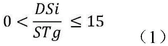
其中,所述抛光层包含具有壳的细小空心颗粒,所述细小空心颗粒的壳的玻璃化转变温度(Tg)为110℃或以下,并且所述抛光层满足以下关系式(1):Wherein, the polishing layer contains fine hollow particles having shells, the glass transition temperature (Tg) of the shells of the fine hollow particles is 110° C. or less, and the polishing layer satisfies the following relational expression (1):

在上述关系式中,DSi是相对于所述抛光层总重量的Si含量(ppmw,按重量计的百万分之一),STg是所述细小空心颗粒的壳的玻璃化转变温度(℃),并且DSi/STg是不包括单位的值之间的比例。In the above relationship, DSi is the Si content (ppmw, parts per million by weight) relative to the total weight of the polishing layer, and STg is the glass transition temperature (°C) of the shell of the fine hollow particles , and DSi/STg is the ratio between values excluding units.
根据另一实施方案,提供了一种制备抛光垫的方法,其包括:制备包含氨基甲酸酯类预聚物的第一原料组合物;制备包含固化剂的第二原料组合物;制备包含具有壳的细小空心颗粒的第三原料组合物;将所述第一原料组合物与所述第二原料组合物和所述第三原料组合物依次或同时混合以制备原料混合物;和将所述原料混合物注入模具中并进行固化以获得抛光层,其中,所述细小空心颗粒的壳的玻璃化转变温度(Tg)为110℃或以下,并且所述抛光层满足上述关系式(1)。According to another embodiment, there is provided a method of preparing a polishing pad, comprising: preparing a first raw material composition comprising a urethane-based prepolymer; preparing a second raw material composition comprising a curing agent; a third raw material composition of fine hollow particles; mixing the first raw material composition with the second raw material composition and the third raw material composition sequentially or simultaneously to prepare a raw material mixture; and mixing the raw material mixture It was poured into a mold and cured to obtain a polishing layer in which the glass transition temperature (Tg) of the shell of the fine hollow particles was 110° C. or less, and the polishing layer satisfies the above-mentioned relational expression (1).
根据又一实施方案,提供了一种制备半导体器件的方法,其包括使用抛光垫抛光半导体衬底的表面,其中,所述抛光垫包括抛光层,所述抛光层包含具有壳的细小空心颗粒,所述细小空心颗粒的壳的玻璃化转变温度(Tg)为110℃或以下,并且所述抛光层满足上述关系式(1)。According to yet another embodiment, there is provided a method of making a semiconductor device comprising polishing a surface of a semiconductor substrate using a polishing pad, wherein the polishing pad includes a polishing layer comprising fine hollow particles having a shell, The glass transition temperature (Tg) of the shell of the fine hollow particles is 110° C. or less, and the polishing layer satisfies the above-mentioned relational expression (1).
本发明的有益效果The beneficial effects of the present invention
根据实施方案的抛光垫包含具有壳的细小空心颗粒,通过调节所述壳的玻璃化转变温度(Tg),从而控制所述壳的硬度和抛光层表面上的孔的形状。由于所述抛光层中的Si含量可调节,从而可以防止由硬质添加剂引起的半导体衬底的表面损伤。The polishing pad according to the embodiment comprises fine hollow particles having a shell, the hardness of the shell and the shape of the pores on the surface of the polishing layer are controlled by adjusting the glass transition temperature (Tg) of the shell. Since the Si content in the polishing layer can be adjusted, surface damage of the semiconductor substrate caused by the hard additive can be prevented.
因此,所述抛光垫可以在CMP工艺期间提供高的抛光速率,同时能够使诸如在半导体衬底表面上的划痕等的缺陷的发生率最小化。Accordingly, the polishing pad can provide a high polishing rate during a CMP process while minimizing the incidence of defects such as scratches on the surface of the semiconductor substrate.
因此,可以将所述抛光垫应用于包括CMP工艺的制备半导体器件的工艺中,以提供高质量的半导体器件。Therefore, the polishing pad can be applied in a process of fabricating a semiconductor device including a CMP process to provide a high-quality semiconductor device.
具体实施方式Detailed ways
在下文中,将详细描述本发明。Hereinafter, the present invention will be described in detail.
在以下实施方案的描述中,在提到每个层、垫或片在另一层、垫或片“之上”或“之下”形成时,不仅可指一个元件“直接”在另一元件之上或之下形成,还可指一个元件“间接”在另一元件之上或之下形成,另一个或多个元件介于它们之间。In the description of the following embodiments, references to each layer, pad or sheet being formed "on" or "under" another layer, pad or sheet may not only mean that one element is "directly" on another element Formed over or under can also mean that one element is formed "indirectly" over or under another element with another element or elements interposed therebetween.
另外,除非另有说明,否则本文所使用的组分的物理性质、尺寸等有关的所有数值范围应理解为由术语“约”修饰。Additionally, all numerical ranges relating to the physical properties, dimensions, etc. of the components used herein are understood to be modified by the term "about" unless otherwise indicated.
抛光垫polishing pad
根据一个实施方案的抛光垫包括抛光层,A polishing pad according to one embodiment includes a polishing layer,
其中,所述抛光层包含具有壳的细小空心颗粒,所述细小空心颗粒的壳的玻璃化转变温度(Tg)为110℃或以下,并且所述抛光层满足以下关系式(1):Wherein, the polishing layer contains fine hollow particles having shells, the glass transition temperature (Tg) of the shells of the fine hollow particles is 110° C. or less, and the polishing layer satisfies the following relational expression (1):

在上述关系式中,DSi是相对于所述抛光层总重量的Si含量(ppmw,按重量计的百万分之一),STg是所述细小空心颗粒的壳的玻璃化转变温度(℃),并且DSi/STg是不包括单位的值之间的比例。In the above relationship, DSi is the Si content (ppmw, parts per million by weight) relative to the total weight of the polishing layer, and STg is the glass transition temperature (°C) of the shell of the fine hollow particles , and DSi/STg is the ratio between values excluding units.
在上述关系式(1)中,DSi/STg,例如,可为1至10、1至8、1至5、1至3、3至15、5至15、7至15、3至10、或3至7。具体地,在上述关系式(1)中,DSi/STg可为1至5。In the above relationship (1), DSi/STg, for example, may be 1 to 10, 1 to 8, 1 to 5, 1 to 3, 3 to 15, 5 to 15, 7 to 15, 3 to 10, or 3 to 7. Specifically, in the above relational formula (1), DSi/STg may be 1 to 5.
如果所述表示所述细小空心颗粒的壳的玻璃化转变温度(Tg)与所述抛光层中的Si含量之间的关系的关系式(1)的值在所述优选范围内,则可以防止在抛光垫的制备工艺中微孔变形,从而在CMP工艺期间保证了用于浆料的平滑流道,同时使诸如可能发生在半导体衬底表面上的划痕等的缺陷的发生率最小化。If the value of the relational formula (1) representing the relation between the glass transition temperature (Tg) of the shell of the fine hollow particles and the Si content in the polishing layer is within the preferred range, it is possible to prevent The pores are deformed during the polishing pad preparation process, thereby ensuring smooth flow paths for the slurry during the CMP process, while minimizing the incidence of defects such as scratches that may occur on the surface of the semiconductor substrate.
抛光层polishing layer
所述抛光层包括聚氨酯树脂并且可以是多孔的。The polishing layer includes a polyurethane resin and may be porous.
所述氨基甲酸酯类聚合物可以通过氨基甲酸酯类预聚物与固化剂之间的反应来形成。The urethane-based polymer may be formed by a reaction between a urethane-based prepolymer and a curing agent.
具体地,所述抛光层可以由包含氨基甲酸酯类预聚物、固化剂、细小空心颗粒和其他添加剂的组合物形成。Specifically, the polishing layer may be formed of a composition including a urethane-based prepolymer, a curing agent, fine hollow particles and other additives.
细小空心颗粒fine hollow particles
所述抛光层包含具有壳的细小空心颗粒。The polishing layer contains fine hollow particles with shells.
所述细小空心颗粒在所述抛光层的表面(即抛光表面)上形成微孔。如果所述壳的硬度高,则它们可能会损坏与它们相互作用的半导体衬底的表面。因此,有必要调节所述壳的硬度,这可以通过调节所述壳的玻璃化转变温度(Tg)来实现。即,通过降低所述壳的玻璃化转变温度,可以在CMP工艺期间使诸如在半导体衬底表面上的划痕等的缺陷的发生率最小化。The fine hollow particles form micropores on the surface of the polishing layer (ie, the polishing surface). If the shells are of high hardness, they may damage the surface of the semiconductor substrate with which they interact. Therefore, it is necessary to adjust the hardness of the shell, which can be achieved by adjusting the glass transition temperature (Tg) of the shell. That is, by lowering the glass transition temperature of the shell, the incidence of defects such as scratches on the surface of the semiconductor substrate can be minimized during the CMP process.
同时,如果所述壳的玻璃化转变温度太低,则在制备工艺中所述细小空心颗粒之间可能发生熔合。另外,由于所述颗粒的变形和破裂,在所述抛光层的表面上形成的微孔可能变形或被去除,从而难以确保用于浆料的平滑流道。Meanwhile, if the glass transition temperature of the shell is too low, fusion between the fine hollow particles may occur during the production process. In addition, due to the deformation and breakage of the particles, micropores formed on the surface of the polishing layer may be deformed or removed, making it difficult to ensure a smooth flow path for the slurry.
因此,需要将所述壳的玻璃化转变温度调节至特定范围以解决上述问题。Therefore, it is necessary to adjust the glass transition temperature of the shell to a specific range in order to solve the above-mentioned problems.
在所述实施方案的抛光垫中,所述细小空心颗粒的壳的玻璃化转变温度(Tg)为110℃或以下。In the polishing pad of the embodiment, the glass transition temperature (Tg) of the shell of the fine hollow particles is 110° C. or less.
例如,所述细小空心颗粒的壳的玻璃化转变温度(Tg)可以是70℃至110℃、80℃至110℃、90℃至110℃、100℃至110℃、70℃至100℃、70℃至90℃、或80℃至100℃。具体地,所述细小空心颗粒的壳的玻璃化转变温度(Tg)可以是70℃至90℃。For example, the glass transition temperature (Tg) of the shell of the fine hollow particles may be 70°C to 110°C, 80°C to 110°C, 90°C to 110°C, 100°C to 110°C, 70°C to 100°C, 70°C °C to 90 °C, or 80 °C to 100 °C. Specifically, the glass transition temperature (Tg) of the shell of the fine hollow particles may be 70°C to 90°C.
在所述优选范围内,可以防止在制备抛光垫的工艺中的微孔变形,从而确保浆料的平滑流道,同时在CMP工艺期间使诸如可能在半导体衬底表面上出现的划痕等的缺陷最小化。Within the preferred range, deformation of the micropores in the process of preparing the polishing pad can be prevented, thereby ensuring a smooth flow path of the slurry, and at the same time making it possible to prevent problems such as scratches that may occur on the surface of the semiconductor substrate during the CMP process. Defects are minimized.
所述细小空心颗粒的平均粒径可以为10μm至100μm、10μm至70μm、10μm至50μm、30μm至100μm、30μm至70μm、或30μm至60μm。具体地,所述细小空心颗粒的平均粒径可以为10μm至70μm。更具体地,所述细小空心颗粒的平均粒径可以为30μm至60μm。在所述优选范围内,更有利于在合适的浆料流速下改善所述CMP工艺的性能。The fine hollow particles may have an average particle diameter of 10 μm to 100 μm, 10 μm to 70 μm, 10 μm to 50 μm, 30 μm to 100 μm, 30 μm to 70 μm, or 30 μm to 60 μm. Specifically, the fine hollow particles may have an average particle diameter of 10 μm to 70 μm. More specifically, the fine hollow particles may have an average particle diameter of 30 μm to 60 μm. Within the preferred range, it is more beneficial to improve the performance of the CMP process at a suitable slurry flow rate.
所述细小空心颗粒的壳的厚度可以为0.01μm至1.5μm。例如,可以是0.05μm至1μm。由于所述细小空心颗粒具有厚度在上述范围内的壳,因此可以在所述抛光层中形成合适的孔结构,从而赋予合适的硬度以改善所述抛光垫的表面的抛光性能。The thickness of the shell of the fine hollow particles may be 0.01 μm to 1.5 μm. For example, it may be 0.05 μm to 1 μm. Since the fine hollow particles have shells with a thickness within the above range, a suitable pore structure can be formed in the polishing layer, thereby imparting suitable hardness to improve the polishing performance of the surface of the polishing pad.
在这种情况下,所述细小空心颗粒的平均粒径是指包含所述细小空心颗粒的壳的厚度在内的总直径。更具体地,在制备抛光垫的过程中,所述细小空心颗粒可被加热而膨胀。在这种情况下,所述细小空心颗粒的平均粒径可以是这种膨胀后的平均粒径。In this case, the average particle diameter of the fine hollow particles refers to the total diameter including the thickness of the shells of the fine hollow particles. More specifically, during the preparation of the polishing pad, the fine hollow particles may be heated to expand. In this case, the average particle diameter of the fine hollow particles may be this expanded average particle diameter.
所述细小空心颗粒可在其中包含气相或液相发泡剂。即,所述气相或液相发泡剂可被所述壳包封在所述细小空心颗粒内部。当被加热时,这种气相或液相发泡剂可以热膨胀或汽化以增加其体积,由此可以使所述壳膨胀。因此,所述细小空心颗粒的壳可以由在被加热时变软的材料制成。The fine hollow particles may contain a gas-phase or liquid-phase blowing agent therein. That is, the gas-phase or liquid-phase blowing agent may be encapsulated inside the fine hollow particles by the shell. When heated, this gas phase or liquid phase blowing agent can thermally expand or vaporize to increase its volume, thereby expanding the shell. Thus, the shells of the fine hollow particles can be made of a material that softens when heated.
例如,所述细小空心颗粒的壳可以包含热塑性树脂。具体地,它们可以包含选自偏二氯乙烯类共聚物、丙烯腈类共聚物、甲基丙烯腈类共聚物和丙烯酸类共聚物中的至少一种。For example, the shells of the fine hollow particles may contain a thermoplastic resin. Specifically, they may contain at least one selected from the group consisting of vinylidene chloride-based copolymers, acrylonitrile-based copolymers, methacrylonitrile-based copolymers, and acrylic copolymers.
另外,所述细小空心颗粒可在其中包含具有低分子量的烃。具体地,所述细小空心颗粒可以在其中包含具有1至7个碳原子的烃。所述具有1至7个碳原子的烃可以是乙烷、乙烯、丙烷、丙烯、正丁烷、异丁烷、丁烯、异丁烯、正戊烷、异戊烷、新戊烷、正己烷和庚烷中的至少一种。In addition, the fine hollow particles may contain hydrocarbons having a low molecular weight therein. Specifically, the fine hollow particles may contain hydrocarbons having 1 to 7 carbon atoms therein. The hydrocarbon having 1 to 7 carbon atoms may be ethane, ethylene, propane, propylene, n-butane, isobutane, butene, isobutene, n-pentane, isopentane, neopentane, n-hexane and At least one of heptane.
相对于所述抛光层的总重量,所述细小空心颗粒的用量可以为0.1重量%至3重量%。或者,相对于所述抛光层的总重量,所述细小空心颗粒的用量可以为1重量%至2重量%。在所述优选范围内,更有利于实施能够提高CMP工艺性能的浆料流速。The fine hollow particles may be used in an amount of 0.1 wt % to 3 wt % with respect to the total weight of the polishing layer. Alternatively, the fine hollow particles may be used in an amount of 1% to 2% by weight relative to the total weight of the polishing layer. Within the preferred range, it is more favorable to implement a slurry flow rate that can improve the performance of the CMP process.
所述抛光层包括多个微孔。具体地,所述微孔可以由所述细小空心颗粒形成。因此,所述微孔的平均直径可以与所述细小空心颗粒的平均粒径相同。The polishing layer includes a plurality of micropores. Specifically, the micropores may be formed by the fine hollow particles. Therefore, the average diameter of the micropores may be the same as the average particle diameter of the fine hollow particles.
所述微孔可以具有敞开孔或封闭孔的结构。具体地,所述抛光层具有暴露于外部的具有敞开孔结构的多个微孔,其中所述微孔可以来源于所述细小空心颗粒。更具体地,在修整所述抛光层的表面期间,所述细小空心颗粒的壳被部分切割,从而可以形成具有所述敞开孔结构的微孔。The micropores may have an open-pore or closed-pore structure. Specifically, the polishing layer has a plurality of micropores with an open pore structure exposed to the outside, wherein the micropores may be derived from the fine hollow particles. More specifically, during the trimming of the surface of the polishing layer, the shells of the fine hollow particles are partially cut so that micropores having the open-pore structure can be formed.
即,所述细小空心颗粒在所述抛光层的表面上形成具有敞开孔结构的微孔,其在CMP工艺期间用作施加在所述抛光层上的浆料的微流体通道。That is, the fine hollow particles form micropores with an open pore structure on the surface of the polishing layer, which serve as microfluidic channels for the slurry applied on the polishing layer during the CMP process.
所述抛光层的表面(即抛光表面)的面积中的所述微孔的总面积可以为30%至60%、35%至50%或35%至43%。The total area of the micropores in the area of the surface of the polishing layer (ie, the polishing surface) may be 30% to 60%, 35% to 50%, or 35% to 43%.
此外,相对于所述抛光层的总体积,所述抛光层可包含20体积%至70体积%的微孔。即,所述抛光层的孔隙率可以为20体积%至70体积%。In addition, the polishing layer may contain 20 to 70 vol % of micropores with respect to the total volume of the polishing layer. That is, the porosity of the polishing layer may be 20% to 70% by volume.
另外,所述抛光层可以在其表面上具有用于机械抛光的凹槽。所述凹槽可以具有机械抛光所需的深度、宽度和间隔,没有特别限制。In addition, the polishing layer may have grooves for mechanical polishing on its surface. The grooves may have depths, widths and intervals required for mechanical polishing without particular limitations.
抛光层的特性Characteristics of the polishing layer
在根据所述实施方案的抛光垫中,所述抛光层中的Si含量可以小于1,000ppmw。所述Si的含量是基于重量的。即,当所述抛光层的总重量为100重量%时,所述抛光层中的Si含量可以小于0.1重量%。In the polishing pad according to the embodiment, the Si content in the polishing layer may be less than 1,000 ppmw. The Si content is based on weight. That is, when the total weight of the polishing layer is 100 wt %, the Si content in the polishing layer may be less than 0.1 wt %.
例如,所述抛光层中的Si含量可以小于800ppmw、小于700ppmw、小于600ppmw、小于500ppmw或小于400ppmw。具体地,所述抛光层中的Si含量可以小于500ppmw。或者,所述抛光层中的Si含量可以为100ppmw至900ppmw、100ppmw至700ppmw或100ppmw至500ppmw。For example, the Si content in the polishing layer may be less than 800 ppmw, less than 700 ppmw, less than 600 ppmw, less than 500 ppmw, or less than 400 ppmw. Specifically, the Si content in the polishing layer may be less than 500 ppmw. Alternatively, the Si content in the polishing layer may be 100 ppmw to 900 ppmw, 100 ppmw to 700 ppmw, or 100 ppmw to 500 ppmw.
在这种情况下,可以通过ICP分析来测量所述抛光层中的Si含量。In this case, the Si content in the polishing layer can be measured by ICP analysis.
所述抛光层中的Si可以来源于各种来源。例如,其可以来源于在制备所述细小中空颗粒中所用的硅类脱模粉末,例如,SiO2粉末等。或者,它可以来源于在制备所述抛光层中使用的硅类添加剂。因此,通过调节所述抛光层中的Si含量至上述范围,可以在使用所述抛光垫的CMP工艺期间使诸如在半导体衬底表面上的划痕等的缺陷的发生率最小化。The Si in the polishing layer can be derived from various sources. For example, it may be derived from a silicon-based mold release powder used in the preparation of the fine hollow particles, eg, SiO 2 powder, and the like. Alternatively, it may be derived from silicon-based additives used in the preparation of the polishing layer. Therefore, by adjusting the Si content in the polishing layer to the above range, the incidence of defects such as scratches on the surface of the semiconductor substrate can be minimized during the CMP process using the polishing pad.
作为具体实例,所述细小空心颗粒的壳的玻璃化转变温度可以为70℃至110℃,并且相对于所述抛光层的总重量,所述Si的含量可以小于1,000ppmw。作为另一个具体实例,所述细小空心颗粒的壳的玻璃化转变温度可以为70℃至90℃,并且相对于所述抛光层的总重量,所述Si的含量可以小于500ppmw。As a specific example, the glass transition temperature of the shell of the fine hollow particles may be 70°C to 110°C, and the content of Si may be less than 1,000 ppmw with respect to the total weight of the polishing layer. As another specific example, the glass transition temperature of the shell of the fine hollow particles may be 70°C to 90°C, and the content of Si may be less than 500 ppmw relative to the total weight of the polishing layer.
所述抛光层的厚度可以是0.8mm至5.0mm、1.0mm至4.0mm、1.0mm至3.0mm、1.5mm至2.5mm、1.7mm至2.3mm或2.0mm至2.1mm。在上述范围内,作为抛光垫的基本物理性质可以充分展现,同时上部和下部之间的微孔的粒径变化最小。The thickness of the polishing layer may be 0.8 mm to 5.0 mm, 1.0 mm to 4.0 mm, 1.0 mm to 3.0 mm, 1.5 mm to 2.5 mm, 1.7 mm to 2.3 mm, or 2.0 mm to 2.1 mm. Within the above range, the basic physical properties as a polishing pad can be sufficiently exhibited while the particle size variation of the micropores between the upper and lower portions is minimal.
所述抛光层的表面硬度可以为50肖氏D至70肖氏D。例如,所述抛光层的表面硬度可以为50肖氏D至60肖氏D、60肖氏D至70肖氏D或55肖氏D至65肖氏D。The surface hardness of the polishing layer may be 50 Shore D to 70 Shore D. For example, the surface hardness of the polishing layer may be 50 Shore D to 60 Shore D, 60 Shore D to 70 Shore D, or 55 Shore D to 65 Shore D.
所述抛光垫对钨层的抛光速率(或去除速率)可以为

支撑层support layer
另外,所述抛光垫可进一步包括设置在所述抛光层的一侧上的支撑层。In addition, the polishing pad may further include a support layer disposed on one side of the polishing layer.
所述支撑层用于支撑所述抛光层并吸收和分散施加至所述抛光层上的冲击力。因此,所述支撑层的硬度可以小于所述抛光层的硬度。The support layer is used to support the polishing layer and absorb and disperse the impact force applied to the polishing layer. Therefore, the hardness of the support layer may be smaller than that of the polishing layer.
所述支撑层可以处于包含微孔的多孔结构中。例如,所述支撑层可以由无纺布或绒面革组成。The support layer may be in a porous structure containing micropores. For example, the support layer may consist of nonwoven or suede.
粘合剂层adhesive layer
所述抛光垫可以进一步包括介于所述抛光层和支撑层之间的粘合剂层。The polishing pad may further include an adhesive layer between the polishing layer and the support layer.
所述粘合剂层用于将所述抛光层和所述支撑层彼此粘合。The adhesive layer serves to bond the polishing layer and the support layer to each other.
所述粘合剂层可以包括热熔粘合剂。所述热熔粘合剂可以是选自聚氨酯树脂、聚酯树脂、乙烯-乙酸乙烯酯树脂、聚酰胺树脂和聚烯烃树脂中的至少一种。具体地,所述热熔粘合剂可以是选自聚氨酯树脂和聚酯树脂中的至少一种。The adhesive layer may include a hot melt adhesive. The hot melt adhesive may be at least one selected from polyurethane resins, polyester resins, ethylene-vinyl acetate resins, polyamide resins, and polyolefin resins. Specifically, the hot melt adhesive may be at least one selected from polyurethane resins and polyester resins.
制备抛光垫的方法Method of making a polishing pad
根据一个实施方案的制备抛光垫的方法包括制备包含氨基甲酸酯类预聚物的第一原料组合物;制备包含固化剂的第二原料组合物;制备包含具有壳的细小空心颗粒的第三原料组合物;将所述第一原料组合物与所述第二原料组合物和所述第三原料组合物依次或同时混合以制备原料混合物;和将所述原料混合物注入模具中并进行固化以获得抛光层,其中,所述细小空心颗粒的壳的玻璃化转变温度(Tg)为110℃或以下,且相对于所述抛光层的总重量,所述Si含量小于1,000ppmw。A method of preparing a polishing pad according to an embodiment includes preparing a first raw material composition including a urethane-based prepolymer; preparing a second raw material composition including a curing agent; preparing a third raw material including fine hollow particles having a shell composition; mixing the first raw material composition with the second raw material composition and the third raw material composition sequentially or simultaneously to prepare a raw material mixture; and injecting the raw material mixture into a mold and curing to obtain A polishing layer, wherein the glass transition temperature (Tg) of the shell of the fine hollow particles is 110° C. or less, and the Si content is less than 1,000 ppmw relative to the total weight of the polishing layer.
所述第一原料中所含的预聚物通常是指具有相对较低分子量的聚合物,其中为了方便在生产过程中模制产品,聚合度被调节至中间水平。例如,所述氨基甲酸酯类预聚物的重均分子量(Mw)可以为500g/mol至3,000g/mol、600g/mol至2,000g/mol、或700g/mol至1,500g/mol。预聚物可以单独成型,或者也可以在与另一种可聚合化合物或固化剂进一步反应后成型,以形成最终产品。The prepolymer contained in the first raw material generally refers to a polymer having a relatively low molecular weight, wherein the degree of polymerization is adjusted to an intermediate level in order to facilitate molding the product during the production process. For example, the urethane-based prepolymer may have a weight average molecular weight (Mw) of 500 g/mol to 3,000 g/mol, 600 g/mol to 2,000 g/mol, or 700 g/mol to 1,500 g/mol. The prepolymer can be formed alone or after further reaction with another polymerizable compound or curing agent to form the final product.
所述氨基甲酸酯类预聚物包括至少一种二异氰酸酯单体和至少一种多元醇的预聚合反应产物。The urethane-based prepolymer includes a prepolymerized reaction product of at least one diisocyanate monomer and at least one polyol.
所述至少一种二异氰酸酯单体可以是至少一种芳香族二异氰酸酯单体和/或至少一种脂肪族二异氰酸酯单体。例如,它可以是选自甲苯二异氰酸酯(toluenediisocyanate,TDI)、1,5-萘二异氰酸酯(naphthalene-1,5-diisocyanate)、对苯二异氰酸酯(p-phenylene diisocyanate)、二甲基联苯二异氰酸酯(tolidine diisocyanate)、二苯基甲烷二异氰酸酯(diphenylmethane diisocyanate,MDI)、六亚甲基二异氰酸酯(hexamethylene diisocyanate,HDI)、二环己基甲烷二异氰酸酯(dicyclohexylmethanediisocyanate,H12MDI)和异佛尔酮二异氰酸酯(isophorone diisocyanate)中的至少一种。The at least one diisocyanate monomer may be at least one aromatic diisocyanate monomer and/or at least one aliphatic diisocyanate monomer. For example, it may be selected from the group consisting of toluene diisocyanate (TDI), 1,5-naphthalene-1,5-diisocyanate, p-phenylene diisocyanate, dimethylbiphenyl diisocyanate Isocyanate (tolidine diisocyanate), diphenylmethane diisocyanate (diphenylmethane diisocyanate, MDI), hexamethylene diisocyanate (hexamethylene diisocyanate, HDI), dicyclohexylmethane diisocyanate (dicyclohexylmethane diisocyanate, H12MDI) and isophorone diisocyanate At least one of (isophorone diisocyanate).
包含在所述第二原料中的固化剂可以是胺化合物和醇化合物中的至少一种。具体地,所述固化剂可以包含选自芳香族胺、脂肪族胺、芳香族醇和脂肪族醇中的至少一种化合物。The curing agent contained in the second raw material may be at least one of an amine compound and an alcohol compound. Specifically, the curing agent may contain at least one compound selected from the group consisting of aromatic amines, aliphatic amines, aromatic alcohols and aliphatic alcohols.
例如,所述固化剂可以是4,4'-亚甲基双(2-氯苯胺)(4,4'-methylenebis(2-chloroaniline),MOCA)、二乙基甲苯二胺(diethyltoluenediamine,DETDA)、二氨基二苯基甲烷(diaminodiphenyl methane)、二氨基二苯砜(diaminodiphenyl sulphone)、间亚二甲苯基二胺(m-xylylene diamine)、异佛尔酮二胺(isophoronediamine)、乙二胺(ethylenediamine)、二亚乙基三胺(diethylenetriamine)、三亚乙基四胺(triethylenetetramine)、聚亚丙基二胺(polypropylenediamine)、聚丙烯三胺(polypropylenetriamine)、乙二醇、二乙二醇、二丙二醇、丁二醇、己二醇、甘油、三羟甲基丙烷(trimethylolpropane)和双(4-氨基-3-氯苯基)甲烷(bis(4-amino-3-chlorophenyl)methane)中的至少一种。For example, the curing agent may be 4,4'-methylenebis(2-chloroaniline) (4,4'-methylenebis(2-chloroaniline), MOCA), diethyltoluenediamine (DETDA) , diaminodiphenyl methane, diaminodiphenyl sulphone, m-xylylene diamine, isophoronediamine, ethylene diamine ( ethylenediamine), diethylenetriamine (diethylenetriamine), triethylenetetramine (triethylenetetramine), polypropylenediamine (polypropylenediamine), polypropylenetriamine (polypropylenetriamine), ethylene glycol, diethylene glycol, diethylene glycol At least one of propylene glycol, butylene glycol, hexylene glycol, glycerol, trimethylolpropane and bis(4-amino-3-chlorophenyl)methane A sort of.
所述第三原料组合物中所含的细小空心颗粒的种类和构型如上所述。The kind and configuration of the fine hollow particles contained in the third raw material composition are as described above.
可以使用脱模剂如SiO2来防止所述细小空心颗粒在储存期间的熔合。然而,这样的脱模剂可能具有高硬度并且可能在CMP工艺期间损坏半导体衬底的表面。A mold release agent such as SiO2 can be used to prevent fusion of the fine hollow particles during storage. However, such release agents may have high hardness and may damage the surface of the semiconductor substrate during the CMP process.
因此,在所述第三原料组合物的制备中使用的细小空心颗粒中的SiO2的含量可以为10重量%或以下,7重量%或以下,5重量%或以下,3重量%或以下,或1重量%或以下。Therefore, the content of SiO 2 in the fine hollow particles used in the preparation of the third raw material composition may be 10 wt % or less, 7 wt % or less, 5 wt % or less, 3 wt % or less, or 1 wt% or less.
具体地,在所述第三原料组合物的制备中的细小空心颗粒可以包含5重量%或以下的SiO2。Specifically, the fine hollow particles in the preparation of the third raw material composition may contain 5 wt % or less of SiO 2 .
另外,制备所述原料混合物的步骤可以通过将所述第一原料组合物与所述第二原料组合物混合,然后再与所述第三原料组合物进一步混合,或通过将所述第一原料组合物与所述第三原料组合物混合,然后再与所述第二原料组合物混合。In addition, the step of preparing the raw material mixture may be performed by mixing the first raw material composition with the second raw material composition and then further mixing with the third raw material composition, or by mixing the first raw material composition The composition is mixed with the third feedstock composition and then with the second feedstock composition.
另外,制备所述原料混合物的步骤可以在50℃至150℃的条件下进行。如果需要,可以在真空消泡条件下进行。In addition, the step of preparing the raw material mixture may be performed under a condition of 50°C to 150°C. If desired, it can be carried out under vacuum defoaming conditions.
所述将所述原料混合物注入模具中并进行固化的步骤可以在60℃至120℃的温度条件和50kg/m2至200kg/m2的压力条件下进行。The step of injecting the raw material mixture into a mold and curing may be performed under a temperature condition of 60° C. to 120° C. and a pressure condition of 50 kg/m 2 to 200 kg/m 2 .
另外,上述制备方法还可进一步包括切割由此获得的抛光垫的表面、在其表面上加工凹槽、与下部结合、检查、包装等步骤。这些步骤可以以制备抛光垫的常规方式进行。In addition, the above-mentioned preparation method may further include the steps of cutting the surface of the polishing pad thus obtained, processing grooves on the surface, bonding with the lower portion, inspecting, packaging, and the like. These steps can be performed in a conventional manner for preparing polishing pads.
由于所述抛光垫包括具有壳的细小空心颗粒,通过调节所述壳的玻璃化转变温度(Tg),从而控制所述壳的硬度和抛光层表面上的微孔的形状。由于所述抛光层中的Si含量可调节,从而可以防止由硬质添加剂引起的半导体衬底的表面损伤。因此,所述抛光垫可以在CMP工艺期间提供高的抛光速率,同时能够使诸如在半导体衬底表面上的划痕等的缺陷的发生率最小化。Since the polishing pad includes fine hollow particles with shells, the hardness of the shells and the shape of pores on the surface of the polishing layer are controlled by adjusting the glass transition temperature (Tg) of the shells. Since the Si content in the polishing layer can be adjusted, surface damage of the semiconductor substrate caused by the hard additive can be prevented. Accordingly, the polishing pad can provide a high polishing rate during a CMP process while minimizing the incidence of defects such as scratches on the surface of the semiconductor substrate.
制备半导体器件的方法Method of making a semiconductor device
根据一个实施方案的用于制备半导体器件的方法包括使用根据所述实施方案的抛光垫来抛光半导体衬底的表面。A method for fabricating a semiconductor device according to one embodiment includes polishing a surface of a semiconductor substrate using the polishing pad according to the embodiment.
即,根据一个实施方案的用于制备半导体器件的方法包括使用抛光垫抛光半导体衬底的表面,其中,所述抛光垫包括抛光层,所述抛光层包含具有壳的细小空心颗粒,所述细小空心颗粒的壳的玻璃化转变温度(Tg)为110℃或以下,并且,相对于所述抛光层的总重量,所述Si的含量小于1,000ppmw。That is, a method for producing a semiconductor device according to one embodiment includes polishing a surface of a semiconductor substrate using a polishing pad, wherein the polishing pad includes a polishing layer including fine hollow particles having shells, the fine The glass transition temperature (Tg) of the shell of the hollow particles is 110° C. or less, and the Si content is less than 1,000 ppmw with respect to the total weight of the polishing layer.
具体地,当将根据所述实施方案的抛光垫固定到压板上时,在所述抛光垫上布置半导体衬底。在这种情况下,所述半导体衬底的表面与所述抛光垫的抛光表面直接接触。可以将抛光浆料喷射到所述抛光垫上以进行抛光。此后,所述半导体衬底和所述抛光垫相对于彼此旋转,从而抛光所述半导体衬底的表面。Specifically, when the polishing pad according to the embodiment is fixed to the platen, a semiconductor substrate is arranged on the polishing pad. In this case, the surface of the semiconductor substrate is in direct contact with the polishing surface of the polishing pad. A polishing slurry can be sprayed onto the polishing pad for polishing. Thereafter, the semiconductor substrate and the polishing pad are rotated relative to each other, thereby polishing the surface of the semiconductor substrate.
实施本发明的实施例IMPLEMENTING EMBODIMENTS OF THE INVENTION
在下文中,将参考实施例来详细描述本发明。阐述这些实施例是为了说明本发明,并且本发明的范围不限于此。Hereinafter, the present invention will be described in detail with reference to Examples. These examples are set forth to illustrate the present invention, and the scope of the present invention is not limited thereto.
实施例和对比例Examples and Comparative Examples
提供一种铸造机,其配备有用于预聚物、固化剂、惰性气体和反应速率控制剂的罐和进料管线。将氨基甲酸酯类预聚物(NCO含量:8.0%,商品名:PUGL-450D,SKC)加入到预聚物罐中,并且向其中按表1所示的量加入细小空心颗粒,所述细小空心颗粒中的气相发泡剂已经由热塑性树脂组成的壳封装。将它们混合24小时。将固化剂(双(4-氨基-3-氯苯基)甲烷,Ishihara)加入所述固化剂罐,并准备氮气(N2)和叔胺类化合物作为反应速率控制剂(商品名:A1,Air Product)。A casting machine is provided that is equipped with tanks and feed lines for prepolymer, curing agent, inert gas, and reaction rate controlling agent. A urethane-based prepolymer (NCO content: 8.0%, trade name: PUGL-450D, SKC) was added to a prepolymer tank, and fine hollow particles were added thereto in an amount shown in Table 1, the fine The gas-phase blowing agent in the hollow particles has been encapsulated by a shell composed of thermoplastic resin. Mix them for 24 hours. A curing agent (bis(4-amino-3-chlorophenyl)methane, Ishihara) was added to the curing agent tank, and nitrogen (N 2 ) and tertiary amine compounds were prepared as reaction rate control agents (trade name: A1, Air Products).
将所述原料在搅拌的同时通过各自的进料管线以恒定速率进料到混合头。在这种情况下,所述反应速率控制剂的进料量为所述原料总进料量的0.5重量%。所述惰性气体(氮气)以下表1中所示的量进料。在将所述氨基甲酸酯类预聚物和固化剂进料的同时调节它们的当量比,其中所述总进料量保持在10kg/min的速率。The raw materials were fed to the mixing head at a constant rate through respective feed lines while stirring. In this case, the feed amount of the reaction rate control agent was 0.5 wt % of the total feed amount of the raw materials. The inert gas (nitrogen) was fed in the amounts shown in Table 1 below. The equivalence ratio of the urethane-based prepolymer and the curing agent was adjusted while the urethane-based prepolymer was fed, wherein the total feeding amount was maintained at a rate of 10 kg/min.
将所述混合的原料注入模具(1000mm×1000mm×3mm)中并固化,以得到固体饼状的成型体。之后,将所述成型体的表面抛光,得到厚度为2mm的抛光层片。此后,在所述抛光层片的表面上形成凹槽,然后通过热熔粘合剂将所述抛光层片与支撑层层压以获得抛光垫。The mixed raw materials were poured into a mold (1000 mm×1000 mm×3 mm) and solidified to obtain a solid cake-shaped molded body. After that, the surface of the molded body was polished to obtain a polishing layer with a thickness of 2 mm. Thereafter, grooves are formed on the surface of the polishing ply, and then the polishing ply is laminated with a support layer by a hot-melt adhesive to obtain a polishing pad.
测试例test case
测试所述实施例和对比例中制备的抛光垫的以下项目。所述结果示于表1中。The polishing pads prepared in the Examples and Comparative Examples were tested for the following items. The results are shown in Table 1.
(1)玻璃化转变温度(Tg)(1) Glass transition temperature (Tg)
用差示扫描量热仪(DSC)以20℃/min的升温速率从40℃至180℃测量所述细小空心颗粒的玻璃化转变温度(Tg)。The glass transition temperature (Tg) of the fine hollow particles was measured with a differential scanning calorimeter (DSC) at a heating rate of 20°C/min from 40°C to 180°C.
(2)抛光层中的Si含量(2) Si content in the polishing layer
使用高频电感耦合等离子体(ICP)通过发光光谱测量所述抛光层样品中的Si含量。The Si content in the polishing layer samples was measured by luminescence spectroscopy using high frequency Inductively Coupled Plasma (ICP).
(3)抛光速率(3) Polishing rate
将所述抛光垫样品安装在CMP机的压板上,安装直径为300mm的硅晶圆,所述硅晶圆上通过CVD工艺沉积了钨(W)层,所述钨层面向所述抛光垫的抛光表面。在将所述钨层以150rpm的速度旋转60秒,并以250mL/min的速率将气相二氧化硅浆料供应到所述抛光垫上的同时,以4.0psi的抛光负荷对所述钨层进行抛光。所述抛光完成后,将所述晶圆与所述载体分离,安装在旋转干燥机中,用蒸馏水洗涤,然后用氮气干燥15秒。The polishing pad sample was installed on the pressing plate of the CMP machine, and a silicon wafer with a diameter of 300 mm was installed, and a tungsten (W) layer was deposited on the silicon wafer by a CVD process, and the tungsten layer faced the surface of the polishing pad. Polished surface. The tungsten layer was polished with a polishing load of 4.0 psi while rotating the tungsten layer at 150 rpm for 60 seconds and supplying fumed silica slurry onto the polishing pad at a rate of 250 mL/min . After the polishing was completed, the wafer was separated from the carrier, mounted in a spin dryer, washed with distilled water, and then dried with nitrogen for 15 seconds.
使用光谱反射仪式厚度测量仪(SI-F80R,Kyence)测量所述抛光前后干燥晶圆的膜厚度的变化。使用以下方程式计算所述抛光速率。The change in film thickness of the dried wafers before and after the polishing was measured using a spectral reflectance thickness meter (SI-F80R, Kyence). The polishing rate is calculated using the following equation.

(4)缺陷数(4) Number of defects
使用所述抛光垫样品进行与上述步骤(3)相同的CMP工艺后,使用晶圆检查设备(AIT XP+,KLA Tencor)观察所述晶圆的表面,以测量通过所述抛光在所述晶圆表面产生的划痕数量(阈值:150,晶粒过滤器阈值:280)。After performing the same CMP process as the above step (3) using the polishing pad sample, the surface of the wafer was observed using a wafer inspection equipment (AIT XP+, KLA Tencor) to measure the surface of the wafer by the polishing. The number of scratches produced on the surface (threshold: 150, grain filter threshold: 280).
[表1][Table 1]

如上表1所示,实施例1-3的抛光垫的细小空心颗粒的壳的Tg为110℃或以下,且Si含量与壳的Tg的比例为15以下,而对比例1-3的抛光垫的壳的Tg和/或Si含量在上述范围以外。As shown in Table 1 above, the Tg of the shell of the fine hollow particles of the polishing pads of Examples 1-3 was 110° C. or less, and the ratio of Si content to the Tg of the shell was 15 or less, while the polishing pads of Comparative Examples 1-3 The Tg and/or Si content of the shell is outside the above range.
测试的结果是,实施例1-3的抛光垫在抛光速率上与对比例1-3的抛光垫相当,但是前者的缺陷率非常低。As a result of the test, the polishing pads of Examples 1-3 were comparable to the polishing pads of Comparative Examples 1-3 in polishing rate, but the defect rate of the former was very low.
同时,对比例4中的细小空心颗粒彼此熔合。因此,不能制备抛光垫。这是因为对比例4的所述细小空心颗粒使用了少量的脱模剂(SiO2),且所述壳的Tg低于70℃,无法防止所述细小空心颗粒之间的熔合。At the same time, the fine hollow particles in Comparative Example 4 were fused to each other. Therefore, the polishing pad could not be prepared. This is because the fine hollow particles of Comparative Example 4 used a small amount of mold release agent (SiO 2 ), and the Tg of the shell was lower than 70° C., which could not prevent fusion between the fine hollow particles.
相反地,即使实施例1至3中的所述细小空心颗粒使用了少量的脱模剂(SiO2),当所述壳的Tg高达70℃以上时,所述细小空心颗粒之间几乎没有熔合,从而所述抛光垫的制备中没有出现问题。On the contrary, even if the fine hollow particles in Examples 1 to 3 used a small amount of mold release agent (SiO 2 ), when the Tg of the shell was as high as 70° C. or more, there was little fusion between the fine hollow particles. , so that there are no problems in the preparation of the polishing pad.
Claims (10)


Applications Claiming Priority (2)
| Application Number | Priority Date | Filing Date | Title |
|---|---|---|---|
| KR1020190035204A KR102174958B1 (en) | 2019-03-27 | 2019-03-27 | Polishing pad which minimizes occurence of defect and preparation method thereof |
| KR10-2019-0035204 | 2019-03-27 |
Publications (2)
| Publication Number | Publication Date |
|---|---|
| CN111745534A true CN111745534A (en) | 2020-10-09 |
| CN111745534B CN111745534B (en) | 2022-03-04 |
Family
ID=72606440
Family Applications (1)
| Application Number | Title | Priority Date | Filing Date |
|---|---|---|---|
| CN202010222116.5A Active CN111745534B (en) | 2019-03-27 | 2020-03-26 | Polishing pads that minimize the incidence of defects and methods of making the same |
Country Status (5)
| Country | Link |
|---|---|
| US (1) | US11000935B2 (en) |
| JP (1) | JP6903258B2 (en) |
| KR (1) | KR102174958B1 (en) |
| CN (1) | CN111745534B (en) |
| TW (1) | TWI728699B (en) |
Cited By (3)
| Publication number | Priority date | Publication date | Assignee | Title |
|---|---|---|---|---|
| CN113246016A (en) * | 2021-06-09 | 2021-08-13 | 广东工业大学 | Multi-layer multifunctional CMP (chemical mechanical polishing) pad and preparation method and application thereof |
| CN115194641A (en) * | 2022-07-29 | 2022-10-18 | 安徽禾臣新材料有限公司 | High-flatness white pad for semiconductor polishing and preparation process thereof |
| CN115431168A (en) * | 2021-06-02 | 2022-12-06 | Skc索密思株式会社 | Polishing pad and method of manufacturing semiconductor device using same |
Families Citing this family (2)
| Publication number | Priority date | Publication date | Assignee | Title |
|---|---|---|---|---|
| KR102502516B1 (en) * | 2021-03-12 | 2023-02-23 | 에스케이엔펄스 주식회사 | Polishing pad, manufacturing method thereof and preparing method of semiconductor device using the same |
| KR102512486B1 (en) * | 2021-05-26 | 2023-03-20 | 에스케이엔펄스 주식회사 | Resin composition for polishing pad and preparation method polishing pad |
Citations (14)
| Publication number | Priority date | Publication date | Assignee | Title |
|---|---|---|---|---|
| US5489233A (en) * | 1994-04-08 | 1996-02-06 | Rodel, Inc. | Polishing pads and methods for their use |
| CN1519894A (en) * | 2003-02-06 | 2004-08-11 | 株式会社东芝 | Polishing pad and method of manufacturing semiconductor device |
| US20090258575A1 (en) * | 2007-08-15 | 2009-10-15 | Richard D Hreha | Chemical Mechanical Polishing Pad and Methods of Making and Using Same |
| JP2009274208A (en) * | 2002-05-23 | 2009-11-26 | Cabot Microelectronics Corp | Microporous polishing pad |
| CN103153538A (en) * | 2010-10-15 | 2013-06-12 | 3M创新有限公司 | Abrasive articles |
| JP2014229778A (en) * | 2013-05-23 | 2014-12-08 | 株式会社東芝 | Polishing pad, polishing method, and method of manufacturing polishing pad |
| JP5959390B2 (en) * | 2012-09-26 | 2016-08-02 | 富士紡ホールディングス株式会社 | Polishing pad sheet, polishing pad, method for producing the same, and polishing method |
| CN106272036A (en) * | 2015-08-17 | 2017-01-04 | 南亚塑胶工业股份有限公司 | Grinding pad for surface planarization processing and manufacturing method thereof |
| JP2017064887A (en) * | 2015-10-02 | 2017-04-06 | 富士紡ホールディングス株式会社 | Polishing pad |
| JP2017177301A (en) * | 2016-03-31 | 2017-10-05 | 富士紡ホールディングス株式会社 | Polishing pad |
| CN107457716A (en) * | 2017-08-29 | 2017-12-12 | 湖北鼎龙控股股份有限公司 | The polishing layer of chemical mechanical polishing pads |
| JP2018051730A (en) * | 2016-09-30 | 2018-04-05 | 富士紡ホールディングス株式会社 | Polishing pad, manufacturing method thereof, and manufacturing method of polished product |
| CN108687654A (en) * | 2017-03-31 | 2018-10-23 | 罗门哈斯电子材料Cmp控股股份有限公司 | Chemical Mechanical Polishing Pads |
| WO2019017366A1 (en) * | 2017-07-19 | 2019-01-24 | 東洋紡株式会社 | Adhesive agent composition |
Family Cites Families (19)
| Publication number | Priority date | Publication date | Assignee | Title |
|---|---|---|---|---|
| US3471276A (en) * | 1966-11-02 | 1969-10-07 | Du Pont | Peripheral abrasive wheels with composite rims |
| JP2002151447A (en) * | 2000-11-13 | 2002-05-24 | Asahi Kasei Corp | Polishing pad |
| JP4313761B2 (en) * | 2002-11-18 | 2009-08-12 | ドン ソン エイ アンド ティ カンパニー リミテッド | Method for producing polyurethane foam containing fine pores and polishing pad produced therefrom |
| JP4039381B2 (en) * | 2004-03-25 | 2008-01-30 | コニカミノルタオプト株式会社 | Glass substrate for information recording medium using glass composition and information recording medium using the same |
| US8075372B2 (en) * | 2004-09-01 | 2011-12-13 | Cabot Microelectronics Corporation | Polishing pad with microporous regions |
| KR100804275B1 (en) * | 2006-07-24 | 2008-02-18 | 에스케이씨 주식회사 | CPM polishing pad comprising a liquid organic core surrounded by a polymer shell and a method of manufacturing the same |
| JP5539339B2 (en) * | 2008-06-23 | 2014-07-02 | サンーゴバン アブレイシブズ,インコーポレイティド | High porosity vitrified superabrasive product and manufacturing method |
| WO2010016486A1 (en) * | 2008-08-08 | 2010-02-11 | 株式会社クラレ | Polishing pad and method for manufacturing the polishing pad |
| US9321947B2 (en) * | 2012-01-10 | 2016-04-26 | Saint-Gobain Abrasives, Inc. | Abrasive products and methods for finishing coated surfaces |
| US8894732B2 (en) * | 2012-05-11 | 2014-11-25 | Rohm And Haas Electronic Materials Cmp Holdings, Inc. | Hollow polymeric-alkaline earth metal oxide composite |
| US20150038066A1 (en) | 2013-07-31 | 2015-02-05 | Nexplanar Corporation | Low density polishing pad |
| JP6315246B2 (en) * | 2014-03-31 | 2018-04-25 | 富士紡ホールディングス株式会社 | Polishing pad and manufacturing method thereof |
| JP6341758B2 (en) * | 2014-05-30 | 2018-06-13 | 株式会社クラレ | Polishing pad |
| JP6600149B2 (en) | 2015-04-03 | 2019-10-30 | 富士紡ホールディングス株式会社 | Polishing pad and manufacturing method thereof |
| US10722999B2 (en) * | 2016-06-17 | 2020-07-28 | Rohm And Haas Electronic Materials Cmp Holdings, Inc. | High removal rate chemical mechanical polishing pads and methods of making |
| JP2018034257A (en) * | 2016-08-31 | 2018-03-08 | 信越半導体株式会社 | dresser |
| KR101949905B1 (en) | 2017-08-23 | 2019-02-19 | 에스케이씨 주식회사 | Porous polyurethane polishing pad and preparation method thereof |
| WO2019050365A1 (en) * | 2017-09-11 | 2019-03-14 | 에스케이씨 주식회사 | Porous polyurethane polishing pad and method for manufacturing same |
| US11577360B2 (en) * | 2019-06-10 | 2023-02-14 | Rohm And Haas Electronic Materials Cmp Holdings, Inc. | Cationic fluoropolymer composite polishing method |
-
2019
- 2019-03-27 KR KR1020190035204A patent/KR102174958B1/en active Active
-
2020
- 2020-02-13 US US16/790,388 patent/US11000935B2/en active Active
- 2020-02-14 TW TW109104786A patent/TWI728699B/en active
- 2020-02-20 JP JP2020026929A patent/JP6903258B2/en active Active
- 2020-03-26 CN CN202010222116.5A patent/CN111745534B/en active Active
Patent Citations (14)
| Publication number | Priority date | Publication date | Assignee | Title |
|---|---|---|---|---|
| US5489233A (en) * | 1994-04-08 | 1996-02-06 | Rodel, Inc. | Polishing pads and methods for their use |
| JP2009274208A (en) * | 2002-05-23 | 2009-11-26 | Cabot Microelectronics Corp | Microporous polishing pad |
| CN1519894A (en) * | 2003-02-06 | 2004-08-11 | 株式会社东芝 | Polishing pad and method of manufacturing semiconductor device |
| US20090258575A1 (en) * | 2007-08-15 | 2009-10-15 | Richard D Hreha | Chemical Mechanical Polishing Pad and Methods of Making and Using Same |
| CN103153538A (en) * | 2010-10-15 | 2013-06-12 | 3M创新有限公司 | Abrasive articles |
| JP5959390B2 (en) * | 2012-09-26 | 2016-08-02 | 富士紡ホールディングス株式会社 | Polishing pad sheet, polishing pad, method for producing the same, and polishing method |
| JP2014229778A (en) * | 2013-05-23 | 2014-12-08 | 株式会社東芝 | Polishing pad, polishing method, and method of manufacturing polishing pad |
| CN106272036A (en) * | 2015-08-17 | 2017-01-04 | 南亚塑胶工业股份有限公司 | Grinding pad for surface planarization processing and manufacturing method thereof |
| JP2017064887A (en) * | 2015-10-02 | 2017-04-06 | 富士紡ホールディングス株式会社 | Polishing pad |
| JP2017177301A (en) * | 2016-03-31 | 2017-10-05 | 富士紡ホールディングス株式会社 | Polishing pad |
| JP2018051730A (en) * | 2016-09-30 | 2018-04-05 | 富士紡ホールディングス株式会社 | Polishing pad, manufacturing method thereof, and manufacturing method of polished product |
| CN108687654A (en) * | 2017-03-31 | 2018-10-23 | 罗门哈斯电子材料Cmp控股股份有限公司 | Chemical Mechanical Polishing Pads |
| WO2019017366A1 (en) * | 2017-07-19 | 2019-01-24 | 東洋紡株式会社 | Adhesive agent composition |
| CN107457716A (en) * | 2017-08-29 | 2017-12-12 | 湖北鼎龙控股股份有限公司 | The polishing layer of chemical mechanical polishing pads |
Cited By (4)
| Publication number | Priority date | Publication date | Assignee | Title |
|---|---|---|---|---|
| CN115431168A (en) * | 2021-06-02 | 2022-12-06 | Skc索密思株式会社 | Polishing pad and method of manufacturing semiconductor device using same |
| CN113246016A (en) * | 2021-06-09 | 2021-08-13 | 广东工业大学 | Multi-layer multifunctional CMP (chemical mechanical polishing) pad and preparation method and application thereof |
| CN115194641A (en) * | 2022-07-29 | 2022-10-18 | 安徽禾臣新材料有限公司 | High-flatness white pad for semiconductor polishing and preparation process thereof |
| CN115194641B (en) * | 2022-07-29 | 2023-08-11 | 安徽禾臣新材料有限公司 | A white pad with high flatness for semiconductor polishing and its preparation process |
Also Published As
| Publication number | Publication date |
|---|---|
| JP6903258B2 (en) | 2021-07-14 |
| US11000935B2 (en) | 2021-05-11 |
| CN111745534B (en) | 2022-03-04 |
| KR20200114085A (en) | 2020-10-07 |
| KR102174958B1 (en) | 2020-11-05 |
| TW202035535A (en) | 2020-10-01 |
| TWI728699B (en) | 2021-05-21 |
| US20200306921A1 (en) | 2020-10-01 |
| JP2020161806A (en) | 2020-10-01 |
Similar Documents
| Publication | Publication Date | Title |
|---|---|---|
| US11724356B2 (en) | Porous polyurethane polishing pad and preparation method thereof | |
| CN111745534B (en) | Polishing pads that minimize the incidence of defects and methods of making the same | |
| US11772236B2 (en) | Porous polishing pad and process for producing the same all fees | |
| FR3055902A1 (en) | CHEMICAL MECHANICAL POLISHING PADS WITH HIGH PLANARIZATION EFFICIENCY AND METHODS OF MANUFACTURE | |
| JP2019024078A (en) | Porous polyurethane polishing pad and method for preparing a semiconductor device using the same | |
| JP2019024079A (en) | Porous polyurethane polishing pad and process for preparing semiconductor device by using the same | |
| US11642752B2 (en) | Porous polyurethane polishing pad and process for preparing the same | |
| JP7285613B2 (en) | Polishing pad, method for manufacturing same, and method for manufacturing semiconductor device using same | |
| JP7196146B2 (en) | Polishing pad, method for manufacturing same, and method for manufacturing semiconductor device using same | |
| KR102304965B1 (en) | Polishing pad, preparation method thereof, and preparation method of semiconductor device using same | |
| TWI792225B (en) | Polishing pad and method for preparing semiconductor device using same | |
| JP7778859B2 (en) | Polishing pad, manufacturing method thereof, and manufacturing method of semiconductor element using the same | |
| US20260077447A1 (en) | Polishing pad, preparation method thereof and preparation method of semiconductor device using the same | |
| TW202536949A (en) | Polishing pad and method of manufacturing a semiconductor device using the same |
Legal Events
| Date | Code | Title | Description |
|---|---|---|---|
| PB01 | Publication | ||
| PB01 | Publication | ||
| SE01 | Entry into force of request for substantive examination | ||
| SE01 | Entry into force of request for substantive examination | ||
| TA01 | Transfer of patent application right |
Effective date of registration: 20210415 Address after: Gyeonggi Do, South Korea Applicant after: SKC SOLMICS Co.,Ltd. Address before: Gyeonggi Do, South Korea Applicant before: SKC Co.,Ltd. |
|
| TA01 | Transfer of patent application right | ||
| GR01 | Patent grant | ||
| GR01 | Patent grant | ||
| CP01 | Change in the name or title of a patent holder |
Address after: Gyeonggi Do, South Korea Patentee after: SK Enpus Co.,Ltd. Address before: Gyeonggi Do, South Korea Patentee before: SKC SOLMICS Co.,Ltd. |
|
| CP01 | Change in the name or title of a patent holder | ||
| TR01 | Transfer of patent right |
Effective date of registration: 20250701 Address after: Chungcheongnam do, South Korea Patentee after: Enpu Shi Co.,Ltd. Country or region after: Republic of Korea Address before: Gyeonggi Do, South Korea Patentee before: SK Enpus Co.,Ltd. Country or region before: Republic of Korea |
|
| TR01 | Transfer of patent right |