CN111982927A - Substrate Processing System - Google Patents
Substrate Processing System Download PDFInfo
- Publication number
- CN111982927A CN111982927A CN202010794112.4A CN202010794112A CN111982927A CN 111982927 A CN111982927 A CN 111982927A CN 202010794112 A CN202010794112 A CN 202010794112A CN 111982927 A CN111982927 A CN 111982927A
- Authority
- CN
- China
- Prior art keywords
- substrate
- image
- inspection
- processing
- wafer
- Prior art date
- Legal status (The legal status is an assumption and is not a legal conclusion. Google has not performed a legal analysis and makes no representation as to the accuracy of the status listed.)
- Granted
Links
Images


Classifications
-
- G—PHYSICS
- G01—MEASURING; TESTING
- G01N—INVESTIGATING OR ANALYSING MATERIALS BY DETERMINING THEIR CHEMICAL OR PHYSICAL PROPERTIES
- G01N21/00—Investigating or analysing materials by the use of optical means, i.e. using sub-millimetre waves, infrared, visible or ultraviolet light
- G01N21/84—Systems specially adapted for particular applications
- G01N21/88—Investigating the presence of flaws or contamination
- G01N21/95—Investigating the presence of flaws or contamination characterised by the material or shape of the object to be examined
- G01N21/956—Inspecting patterns on the surface of objects
- G01N21/95607—Inspecting patterns on the surface of objects using a comparative method
-
- G—PHYSICS
- G01—MEASURING; TESTING
- G01N—INVESTIGATING OR ANALYSING MATERIALS BY DETERMINING THEIR CHEMICAL OR PHYSICAL PROPERTIES
- G01N21/00—Investigating or analysing materials by the use of optical means, i.e. using sub-millimetre waves, infrared, visible or ultraviolet light
- G01N21/84—Systems specially adapted for particular applications
- G01N21/88—Investigating the presence of flaws or contamination
- G01N21/95—Investigating the presence of flaws or contamination characterised by the material or shape of the object to be examined
- G01N21/956—Inspecting patterns on the surface of objects
-
- G—PHYSICS
- G01—MEASURING; TESTING
- G01N—INVESTIGATING OR ANALYSING MATERIALS BY DETERMINING THEIR CHEMICAL OR PHYSICAL PROPERTIES
- G01N21/00—Investigating or analysing materials by the use of optical means, i.e. using sub-millimetre waves, infrared, visible or ultraviolet light
- G01N21/84—Systems specially adapted for particular applications
- G01N21/88—Investigating the presence of flaws or contamination
- G01N21/95—Investigating the presence of flaws or contamination characterised by the material or shape of the object to be examined
- G01N21/9501—Semiconductor wafers
-
- G—PHYSICS
- G03—PHOTOGRAPHY; CINEMATOGRAPHY; ANALOGOUS TECHNIQUES USING WAVES OTHER THAN OPTICAL WAVES; ELECTROGRAPHY; HOLOGRAPHY
- G03F—PHOTOMECHANICAL PRODUCTION OF TEXTURED OR PATTERNED SURFACES, e.g. FOR PRINTING, FOR PROCESSING OF SEMICONDUCTOR DEVICES; MATERIALS THEREFOR; ORIGINALS THEREFOR; APPARATUS SPECIALLY ADAPTED THEREFOR
- G03F1/00—Originals for photomechanical production of textured or patterned surfaces, e.g., masks, photo-masks, reticles; Mask blanks or pellicles therefor; Containers specially adapted therefor; Preparation thereof
- G03F1/68—Preparation processes not covered by groups G03F1/20 - G03F1/50
- G03F1/82—Auxiliary processes, e.g. cleaning or inspecting
- G03F1/84—Inspecting
-
- G—PHYSICS
- G03—PHOTOGRAPHY; CINEMATOGRAPHY; ANALOGOUS TECHNIQUES USING WAVES OTHER THAN OPTICAL WAVES; ELECTROGRAPHY; HOLOGRAPHY
- G03F—PHOTOMECHANICAL PRODUCTION OF TEXTURED OR PATTERNED SURFACES, e.g. FOR PRINTING, FOR PROCESSING OF SEMICONDUCTOR DEVICES; MATERIALS THEREFOR; ORIGINALS THEREFOR; APPARATUS SPECIALLY ADAPTED THEREFOR
- G03F7/00—Photomechanical, e.g. photolithographic, production of textured or patterned surfaces, e.g. printing surfaces; Materials therefor, e.g. comprising photoresists; Apparatus specially adapted therefor
- G03F7/70—Microphotolithographic exposure; Apparatus therefor
- G03F7/70483—Information management; Active and passive control; Testing; Wafer monitoring, e.g. pattern monitoring
- G03F7/70605—Workpiece metrology
- G03F7/70616—Monitoring the printed patterns
- G03F7/7065—Defects, e.g. optical inspection of patterned layer for defects
-
- H—ELECTRICITY
- H10—SEMICONDUCTOR DEVICES; ELECTRIC SOLID-STATE DEVICES NOT OTHERWISE PROVIDED FOR
- H10P—GENERIC PROCESSES OR APPARATUS FOR THE MANUFACTURE OR TREATMENT OF DEVICES COVERED BY CLASS H10
- H10P74/00—Testing or measuring during manufacture or treatment of wafers, substrates or devices
- H10P74/20—Testing or measuring during manufacture or treatment of wafers, substrates or devices characterised by the properties tested or measured, e.g. structural or electrical properties
- H10P74/203—Structural properties, e.g. testing or measuring thicknesses, line widths, warpage, bond strengths or physical defects
-
- H—ELECTRICITY
- H10—SEMICONDUCTOR DEVICES; ELECTRIC SOLID-STATE DEVICES NOT OTHERWISE PROVIDED FOR
- H10P—GENERIC PROCESSES OR APPARATUS FOR THE MANUFACTURE OR TREATMENT OF DEVICES COVERED BY CLASS H10
- H10P74/00—Testing or measuring during manufacture or treatment of wafers, substrates or devices
- H10P74/23—Testing or measuring during manufacture or treatment of wafers, substrates or devices characterised by multiple measurements, corrections, marking or sorting processes
-
- H—ELECTRICITY
- H10—SEMICONDUCTOR DEVICES; ELECTRIC SOLID-STATE DEVICES NOT OTHERWISE PROVIDED FOR
- H10P—GENERIC PROCESSES OR APPARATUS FOR THE MANUFACTURE OR TREATMENT OF DEVICES COVERED BY CLASS H10
- H10P76/00—Manufacture or treatment of masks on semiconductor bodies, e.g. by lithography or photolithography
Landscapes
- Physics & Mathematics (AREA)
- General Physics & Mathematics (AREA)
- General Health & Medical Sciences (AREA)
- Chemical & Material Sciences (AREA)
- Analytical Chemistry (AREA)
- Biochemistry (AREA)
- Life Sciences & Earth Sciences (AREA)
- Health & Medical Sciences (AREA)
- Immunology (AREA)
- Pathology (AREA)
- Investigating Materials By The Use Of Optical Means Adapted For Particular Applications (AREA)
- Testing Or Measuring Of Semiconductors Or The Like (AREA)
- Exposure Of Semiconductors, Excluding Electron Or Ion Beam Exposure (AREA)
- Image Processing (AREA)
Abstract
本发明提供一种基板处理系统。具有对基板实施规定处理的多个处理装置的基板处理系统,拍摄用处理装置处理前的基板的表面来取得第一基板图像,从该第一基板图像抽取规定的特征量,从存储有与各自不同的范围的特征量对应地设定的多个检查方案的存储部,选择与从第一基板图像抽取的特征量对应的检查方案,拍摄用处理装置处理后的基板的表面来取得第二基板图像,基于检查方案和第二基板图像,判断基板有无缺陷。根据本发明,能够进行最佳的检查,并能够抑制精度的偏差。
The present invention provides a substrate processing system. A substrate processing system including a plurality of processing apparatuses that perform predetermined processing on a substrate, acquires a first substrate image by photographing the surface of the substrate before processing by the processing apparatus, extracts predetermined feature quantities from the first substrate image, A storage unit for a plurality of inspection plans set in correspondence with feature values in different ranges, selects the inspection plan corresponding to the feature values extracted from the first substrate image, and captures the image of the surface of the substrate processed by the processing device to obtain the second substrate The image, based on the inspection plan and the second substrate image, determines whether the substrate is defective or not. According to the present invention, an optimum inspection can be performed, and variations in accuracy can be suppressed.
Description
技术领域technical field
本申请基于2015年5月12日在日本申请的特愿2015-097333号,要求优先权,在此引用其内容。This application claims priority based on Japanese Patent Application No. 2015-097333 filed in Japan on May 12, 2015, the content of which is incorporated herein by reference.
本发明涉及检查基板的方法、基板处理系统和存储实行所述基板的检查方法的程序的可读取的计算机存储介质。The present invention relates to a method for inspecting a substrate, a substrate processing system, and a readable computer storage medium storing a program for implementing the method for inspecting a substrate.
背景技术Background technique
例如半导体器件的制造步骤的光刻步骤中,依次进行向作为基板的半导体晶片(以下,称为“晶片”)上涂敷抗蚀剂液来形成抗蚀剂膜的抗蚀剂涂敷处理、将抗蚀剂膜以规定图案曝光的曝光处理、对曝光过的抗蚀剂膜进行显影的显影处理等一系列的处理,并在晶片上形成规定的抗蚀剂图案。上述一系列的处理,在装载处理晶片的各种处理装置或搬送晶片的搬送机构等的作为基板处理系统的涂敷显影处理系统中进行。For example, in a photolithography step of a manufacturing step of a semiconductor device, a resist coating process of applying a resist liquid to a semiconductor wafer (hereinafter, referred to as "wafer") as a substrate to form a resist film is sequentially performed, A predetermined resist pattern is formed on a wafer by a series of treatments such as exposure treatment for exposing the resist film in a predetermined pattern, and development treatment for developing the exposed resist film. The above-mentioned series of processes are performed in a coating and developing process system serving as a substrate processing system, such as various processing apparatuses for loading the processed wafers, or a transport mechanism for transporting the wafers.
在上述的涂敷显影处理系统设置有对晶片进行所谓巨大缺陷的检查的检查装置(专利文献1)。在巨大缺陷检查中,在涂敷显影处理系统进行了规定的处理的晶片,在规定的照明下利用例如CCD线阵传感器等的拍摄装置进行拍摄,取得该晶片的拍摄图像。然后,与以取得的拍摄图像为基准的晶片的图像比较,据此判断是否有缺陷。The above-mentioned coating and developing processing system is provided with an inspection apparatus for inspecting a wafer for so-called giant defects (Patent Document 1). In the giant defect inspection, a wafer subjected to predetermined processing in a coating and developing processing system is photographed under predetermined illumination by an imaging device such as a CCD line sensor, and a photographed image of the wafer is acquired. Then, it is determined whether or not there is a defect based on the comparison with the image of the wafer based on the acquired captured image.
现有技术文献prior art literature
专利文献Patent Literature
专利文献1:日本特开2012-104593号公报。Patent Document 1: Japanese Patent Laid-Open No. 2012-104593.
发明内容SUMMARY OF THE INVENTION
发明想要解决的技术问题Invent the technical problem you want to solve
由此,在上述的巨大缺陷的检查中,设定作为基准的晶片的画像、照明的照度或拍摄速度等的检查方案。但是,为了在光刻步骤中在晶片表面形成各种膜,晶片表面的反射率等的表面状态,在每个步骤中都不同。因此,根据晶片的表面状态,产生巨大缺陷检查的精度的偏差的问题。Thereby, in the inspection of the above-mentioned huge defect, inspection plans such as the image of the wafer, the illuminance of the illumination, the imaging speed, and the like are set as a reference. However, in order to form various films on the wafer surface in the photolithography step, the surface state of the reflectance of the wafer surface and the like differs in each step. Therefore, depending on the surface state of the wafer, there is a problem of variation in the accuracy of the inspection of huge defects.
鉴于上述问题,本发明的目的在于在基板处理系统中适当进行基板的检查。In view of the above-mentioned problems, an object of the present invention is to appropriately perform inspection of substrates in a substrate processing system.
用于解决技术问题的技术方案Technical solutions for solving technical problems
为达到上述目的,本发明为一种基板的检查方法,其用于具有对基板实施规定处理的多个处理装置的基板处理系统,上述基板的检查方法的特征在于:拍摄用上述处理装置处理前的基板的表面来取得第一基板图像,从上述第一基板图像抽取规定的特征量,从存储有与各自不同的范围的上述特征量对应地设定的多个检查方案的存储部,选择与从上述第一基板图像抽取出的上述特征量对应的检查方案,拍摄用上述处理装置处理后的基板的表面来取得第二基板图像,基于上述检查方案和上述第二基板图像,判断基板有无缺陷。In order to achieve the above object, the present invention provides a substrate inspection method for a substrate processing system including a plurality of processing apparatuses that perform predetermined processing on the substrate, wherein the substrate inspection method is characterized in that: before the processing by the processing apparatus for imaging A first substrate image is obtained from the surface of the substrate, a predetermined feature value is extracted from the first substrate image, and a plurality of inspection plans set corresponding to the feature values in different ranges are stored in the storage unit to select the According to the inspection plan corresponding to the feature quantity extracted from the first substrate image, the surface of the substrate processed by the processing device is photographed to obtain a second substrate image, and the presence or absence of the substrate is determined based on the inspection plan and the second substrate image. defect.
根据本发明,首先拍摄用处理站处理前的基板的表面来取得第一基板图像,基于该第一基板图像的特征量选择检查方案,因此基于最适宜的检查方案,能够适当地判断第二基板图像中有无缺陷。因此,与基板的表面状态无关,总是能够进行最佳的检查,并能够抑制巨大缺陷的精度的偏差。According to the present invention, the surface of the substrate before being processed by the processing station is photographed to obtain the first substrate image, and the inspection plan is selected based on the feature quantity of the first substrate image. Therefore, the second substrate can be appropriately determined based on the most suitable inspection plan. There are no defects in the image. Therefore, regardless of the surface state of the substrate, it is possible to always perform optimal inspection, and it is possible to suppress variations in the accuracy of giant defects.
本发明的另一方面为一种基板处理系统,其具有对基板实施规定处理的多个处理装置,上述基板处理系统的特征在于,包括:检查装置,其包括:第一拍摄装置,其拍摄用上述处理装置处理前的基板的表面来取得第一基板图像;特征量抽取部,其从上述第一基板图像抽取规定的特征量;存储部,其存储有与各自不同的范围的上述特征量对应地设定的多个检查方案;方案选择部,其从存储于上述存储部的上述检查方案,选择与由上述特征量抽取部抽取出的特征量对应的检查方案;和第二拍摄装置,其拍摄用上述处理装置处理后的基板的表面来取得第二基板图像;和缺陷判断部,其基于上述选择的检查方案,判断上述第二基板图像中有无缺陷。Another aspect of the present invention is a substrate processing system including a plurality of processing apparatuses that perform predetermined processing on a substrate, wherein the substrate processing system includes an inspection apparatus including a first imaging apparatus for imaging A first substrate image is obtained from the surface of the substrate before being processed by the processing apparatus; a feature value extraction unit that extracts a predetermined feature value from the first substrate image; and a storage unit that stores the feature values corresponding to the respective different ranges a plurality of inspection plans set independently; a plan selection unit that selects an inspection plan corresponding to the feature quantity extracted by the feature quantity extraction unit from the inspection plans stored in the storage unit; and a second imaging device photographing the surface of the substrate processed by the processing apparatus to obtain a second substrate image; and a defect determination unit determining whether or not the second substrate image has defects based on the selected inspection plan.
本发明的另一方面为一种收纳有程序的可读取的计算机存储介质,上述程序在控制基板处理系统的控制部的计算机上运行,以使得通过上述基板处理系统执行上述基板处理系统的基板检查方法。Another aspect of the present invention is a readable computer storage medium storing a program that runs on a computer that controls a control unit of a substrate processing system so that a substrate of the substrate processing system is executed by the substrate processing system. Inspection Method.
发明效果Invention effect
根据本发明,能够在基板处理系统中,适当地进行基板的检查。ADVANTAGE OF THE INVENTION According to this invention, the inspection of a board|substrate can be performed suitably in a board|substrate processing system.
附图说明Description of drawings
图1是表示本实施方式的基板处理系统的构成的概略的平面图。FIG. 1 is a plan view showing a schematic configuration of a substrate processing system according to the present embodiment.
图2是表示本实施方式的基板处理系统的构成的概略的主视图。FIG. 2 is a front view showing the outline of the configuration of the substrate processing system according to the present embodiment.
图3是表示本实施方式的基板处理系统的构成的概略的后视图。FIG. 3 is a rear view showing the outline of the configuration of the substrate processing system according to the present embodiment.
图4是表示检查装置的构成的概略的横截面图。FIG. 4 is a schematic cross-sectional view showing the configuration of the inspection apparatus.
图5是表示检查装置的构成的概略的纵截面图。5 is a longitudinal cross-sectional view showing a schematic configuration of an inspection apparatus.
图6是模式地表示控制装置的构成的概略的框图。FIG. 6 is a block diagram schematically showing the outline of the configuration of the control device.
图7是表示像素值和检查方案的关系的说明图。FIG. 7 is an explanatory diagram showing the relationship between pixel values and inspection schemes.
图8是表示晶片的缺陷检查的步骤的概略的流程图。FIG. 8 is a flowchart showing an outline of a procedure of defect inspection of a wafer.
图9是表示像素值和检查方案的关系的说明图。FIG. 9 is an explanatory diagram showing the relationship between pixel values and inspection schemes.
具体实施方式Detailed ways
以下,对本发明的实施方式进行说明。图1是表示本实施方式的基板处理系统的构成的概略的平面图。图2和图3是表示本实施方式的基板处理系统的构成的概略的主视图和后视图。此外,本实施方式中,以基板处理系统1为对晶片W进行涂敷显影处理的涂敷显影处理系统的情形为例子进行说明。另外,在本说明书和附图中,对于实质上具有同一功能构成的要素标注相同的附图标记,对此省略重复说明。Hereinafter, embodiments of the present invention will be described. FIG. 1 is a plan view showing a schematic configuration of a substrate processing system according to the present embodiment. 2 and 3 are a front view and a rear view showing a schematic configuration of the substrate processing system according to the present embodiment. In addition, in this embodiment, the case where the
如图1所示,基板处理系统1包括搬送收纳有多个晶片的盒C的盒工作站10、具有对晶片W实施规定处理的多个处理装置的处理站11、与处理站11邻接并在与曝光装置12之间的进行晶片W的交接的接口站13一体连接的构成。As shown in FIG. 1 , the
在盒工作站10设置有盒载置台20。在盒载置台20设置多个向基板处理系统1的外部搬送盒C时载置盒C的盒载置板21。The
如图1所示,在盒工作站10设置有在X方向延伸的搬送通路22上可移动的晶片搬送装置23。晶片搬送装置23,在上下方向和垂直轴周围(θ方向)也可移动,在各盒载置板21上的盒C和后述的处理站11的第三块G3的交接装置之间搬送晶片W。As shown in FIG. 1 , the
在处理站11设置有具有各种装置的多个例如4个块G1、G2、G3、G4。例如,在处理站11的正面侧(图1的X方向的负方向侧)设置第一块G1,在处理站11的背面侧(图1的X方向的正方向侧)设置第二块G2。另外,在处理站11的盒工作站10一侧(图1的Y方向的负方向侧)设置第三块G3,在处理站11的接口站13一侧(图1的Y方向的正方向侧)设置第四块G4。A plurality of, for example, four blocks G1 , G2 , G3 , and G4 having various devices are installed in the
例如,在第一块G1中,如图2所示例如从下开始按顺序配置对晶片W进行显影处理的显影处理装置30、在晶片W的抗蚀剂膜的下层形成防反射膜(以下称为“下部防反射膜”)的下部防反射膜形成装置31、对晶片W涂敷抗蚀剂液来形成抗蚀剂膜的抗蚀剂涂敷装置32、在晶片W的抗蚀剂膜的上层形成防反射膜(以下,称为“上部防反射膜”)的上部防反射膜形成装置33。For example, in the first block G1 , as shown in FIG. 2 , for example, developing
例如,显影处理装置30、下部防反射膜形成装置31、抗蚀剂涂敷装置32、上部防反射膜形成装置33分别在水平方向上并列配置3个。此外,上述显影处理装置30、下部防反射膜形成装置31、抗蚀剂涂敷装置32、上部防反射膜形成装置33的个数或配置,能够任意选择。For example, three
在上述显影处理装置30、下部防反射膜形成装置31、抗蚀剂涂敷装置32、上部防反射膜形成装置33中,例如能够进行在晶片W上涂敷规定的涂敷液的旋涂操作。在旋涂操作中,例如从涂敷喷嘴向晶片W上排出涂敷液,同时使晶片W旋转,使涂敷液在晶片W表面扩散。In the above-described
例如,在第二块G2中,如图3所示,进行晶片W的加热或冷却之类的热处理的热处理装置40、用于提高抗蚀剂液和晶片W定影性的粘着装置41、曝光晶片W的外周部的周边曝光装置42在上下方向和水平方向并排设置。上述热处理装置40、粘着装置41、周边曝光装置42的个数和配置,也能够任意选择。For example, in the second block G2, as shown in FIG. 3, a
例如,在第三块G3,从下开始按顺序设置对在处理站11进行处理前的晶片W进行检查的检查装置50、多个交接装置51、52、53、54、55和对经处理站11处理后的晶片W进行检查的检查装置56。另外,在第四块,从下开始按顺序设置多个交接装置60、61、62。对于检查装置50、56的构成,后面进行叙述。For example, in the third block G3, the
如图1所示,在由第一块G1~第四块G4包围的区域中形成晶片搬送区域D。在晶片搬送区域D,例如配置有多个晶片搬送装置70,该晶片搬送装置70具有在Y方向、X方向、θ方向以及上下方向可移动的搬送臂,晶片搬送装置70,在晶片搬送区域内移动,并能够向周围的第一块G1、第二块G2、第三块G3和第四块G4内的规定的装置搬送晶片W。As shown in FIG. 1, the wafer transfer area D is formed in the area|region enclosed by the 1st block G1 - the 4th block G4. In the wafer transfer area D, for example, a plurality of
另外,在晶片搬送区域D,在第三块G3和第四块G4之间设置直线地搬送晶片W的往复搬送装置80。In addition, in the wafer transfer area D, a
往复搬送装置80,例如在图3的Y方向直线地可移动。往复搬送装置80,在支承有晶片的状态下在Y方向移动,能够在第三块G3的交接装置52和第四块G4的交接装置62之间搬送晶片W。The
如图1所示,在第三块G3的X方向的正方向侧的附近设置有晶片搬送装置90。晶片搬送装置90例如具有在X方向、θ方向和上下方向上可移动的搬送臂。晶片搬送装置90,在支承有晶片的状态下上下移动,能够向第三块G3内的各交接装置搬送晶片W。As shown in FIG. 1, the
在接口站13设置有晶片搬送装置100和交接装置101。晶片搬送装置100,例如具有在Y方向、θ方向和上下方向上可移动的搬送臂。晶片搬送装置100,例如在搬送臂支承晶片W,能够在第四块G4的各交接装置、交接装置101和曝光装置12之间搬送晶片。The
接着,对上述检查装置50的构成进行说明。如图4所示,检查装置50具有外壳150。如图5所示,在外壳150内设置有保持晶片W的晶片卡盘151。在外壳150的底面设置有从外壳150内的一端侧(图4中X方向的负方向侧)向另一端侧(图4中X方向的正方向侧)延伸的导轨152。在导轨152上设置有使卡盘151旋转并能够沿导轨152移动的驱动部153。Next, the configuration of the above-mentioned
在外壳150内的另一端侧(图4中X方向的正方向侧)的侧面设置有作为第一拍摄装置的拍摄部160。作为拍摄部160能够使用例如广角型CCD相机。在外壳150的上部中央附近设置有半透半反镜161。半透半反镜161在与拍摄部160相对的位置,以镜面从向铅垂下方的状态向拍摄部160的方向45度向上方倾斜的状态设置。在半透半反镜161的上方设置有照明装置162。半透半反镜161和照明装置162固定在外壳150的内部的上表面。来自照明装置162的照明,透光半透半反镜161向下方照射。因此,由在照明装置162的下方的物体反射的光,再由半透半反镜161反射,由拍摄部160接收。即,拍摄部160,能够拍摄处于由照明装置162形成的照射区域的物体。然后,通过检查装置50的拍摄部160拍摄的晶片W的图像(第一基板图像),输入后述的控制装置200。An
检查装置56具有与检查装置50同样的构成,因此,省略对检查装置56的说明。此外,检查装置56的拍摄部160,作为本发明的第二拍摄装置的工作,由检查装置56的拍摄部160拍摄的晶片W的图像(第二基板图像),也同样地被输入控制装置200。The
在以上的基板处理系统1,如图1所示设置有控制装置200。控制装置200,例如由具有CPU和存储器等的计算机构成,并具有程序存储部(未图示)。在程序存储部存储有控制基于由检查装置50、56拍摄的基板图像进行晶片W的检查的程序。此外,在程序存储部也存储有如下程序:控制上述各种处理装置或搬送装置等的驱动系统的动作,用于实现基板处理系统1的规定的作用、即向晶片W涂敷抗蚀剂液、显影、加热处理、晶片W的交接、各单元的控制等。此外,所述程序是记录在例如计算机可读硬盘(HD)、软盘(FD)、光盘(CD)、磁光盘(MO)、存储卡等计算机可读取的存储介质H中的程序,也可以是从该存储介质H向控制装置200安装的程序。The above
另外,如图6所示,控制装置200具有:从由检查装置50的拍摄部160拍摄的第一基板图像抽取规定的特征量的特征量抽取部210;存储有多个与规定范围的特征量对应地设定的检查方案的存储部21;根据存储于存储部211的多个检查方案,选择与由特征抽取部210抽取的特征量对应的检查方案的方案选择部212;和基于选择的检查方案和由检查装置56的拍摄部160拍摄的第二基板图像判断有无缺陷的缺陷判断部213。另外,在控制装置200还设置有:保存由拍摄部160拍摄的第一基板图像和第二基板图像的图像保存部214;基于由特征量抽取部210抽取的特征量、将保存于图像保存部214的第一基板图像分类为多个组的图像分类部215;将与由图像分类部215分类为各组的多个第一基板图像对应的第二基板图像合成,来生成基准图像的基准图像生成部216;和基于由基准图像生成部216生成的基准图像生成的检查方案,并将其存储在存储部211的检查方案生成部217。In addition, as shown in FIG. 6 , the
由特征量抽取部210抽取的特征量,在本实施方式中例如为基板图像的像素值。然后,在特征量抽取部210中,例如,对基板图像的全部的像素值计算出平均值,求出该平均值作为该基板图像的特征量。此外,本实施方式中,以基板图像为例如256灰度(0~255)的8bit图像的情况为例进行说明。The feature value extracted by the feature
在存储部211,例如,如图7所示存储与不同的范围的像素值对应地设定的例如3种检查方案230、231、232。检查方案230例如在第一基板图像的特征量)(像素值的平均值)为“10~70”的范围时使用,检查方案231、232分别在特征量为“90~140”“200~240”的范围时使用。各检查方案230、231、232例如由用各拍摄部160拍摄时的拍摄条件、成为缺陷检查的基准的基准图像等构成。此外,存储于存储部211的检查方案的个数或检查方案的覆盖的范围能够任意地设定,本实施方式的内部不限于此。In the
在方案选择部212中,从存储部211选择与由特征量抽取部210抽取的特征量对应的检查方案。例如,任意的批量的晶片W在检查装置50中拍摄取得的第一基板图像的特征量为“60”使,通过方案选择部212,从存储部211选择特征量为“10~70”的基板图像对应的检查方案230。In the plan selection unit 212 , an inspection plan corresponding to the feature quantity extracted by the feature
在缺陷判断部213中,基于该检查方案230和第二基板图像判断有无缺陷。具体来说,对第一基板图像的特征量为“60”的晶片W在处理站11完成规定处理时,由检查装置56的拍摄部160拍摄来取得第二基板图像。然后,在缺陷判断部213中,利用基于第一基板图像的特征量“60”选择的检查方案,基于同一晶片W的第二基板图像判断有无缺陷。此外,关于其他的图像保存部214、图像分类部215、基准图像生成部216、检查方案生成部217的功能,后面进行叙述。The
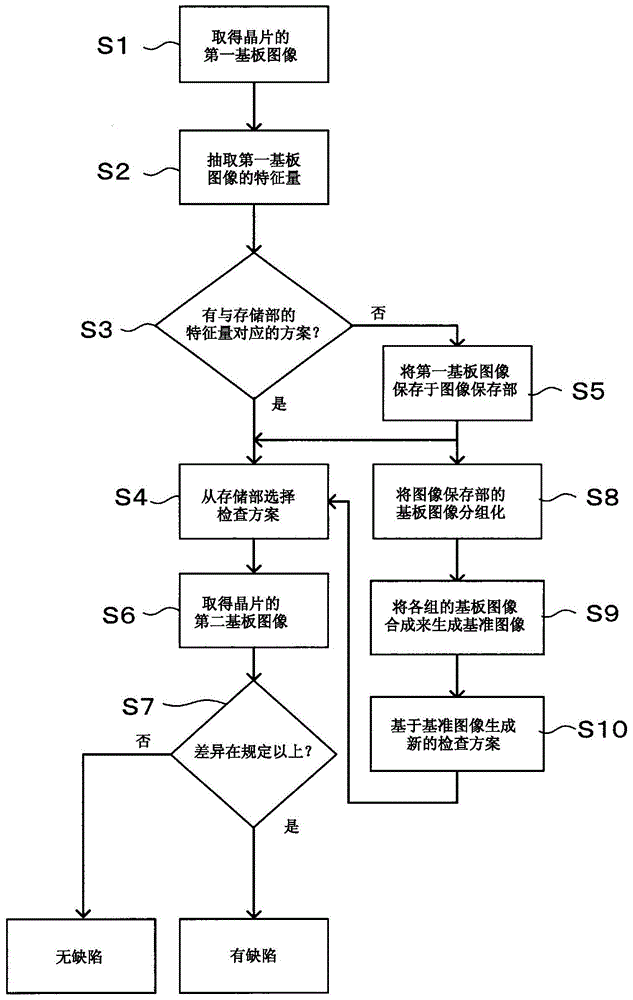
接着,对使用如上构成的基板处理系统1进行的晶片W的处理方案和晶片W的检查方法进行说明。图8是表示上述晶片W的检查方法的主要步骤的例子的流程图,基于该图8对检查方法进行说明。Next, a method for processing the wafer W and a method for inspecting the wafer W by using the
首先,将收纳有同一批的多个晶片W的盒C搬入基板处理系统1的盒工作站10,由晶片搬送装置23将盒C内的各晶片按顺序搬入第三块G3的检查装置50,取得第一基板图像(图8的步骤S1)。接着,在特征量抽取部210中,从该第一基板图像抽取特征量(图8的步骤S2)。然后,如果与第一基板图像的特征量对应的检查方案存在于存储部211,则由方案选择部212选择规定的检查方案(图8的步骤S3、S4)。具体来讲,例如作为特征量的像素值的平均值为“60”时,在方案选择部212中从存储部211选择与特征量“60”对应的检查方案230。另外,例如特征量为“150”,在存储部211内不存在对应的检查方案时(图8的步骤S3的否),特征量为“150”的第一基板图像,保存于图像保存部214(图8的步骤S5),并且选择预先规定的检查方案(图8的步骤S4)。对于在图像保存部214保存第一基板图像后的处理,后面进行叙述。在此,预先规定的检查方案,例如可以为存储于存储部211的多个检查方案中的任意检查方案,例如本实施方式中,检查方案231为作为预先规定的检查方案进行说明。即,第一基板图像的特征量为“150”时,存储部211内不存在对应的检查方案,因此,选择预先规定的检查方案231。First, the cassette C containing a plurality of wafers W in the same batch is loaded into the
接着,晶片W被搬送到第二块G2的热处理装置40并进行温度调节处理。其后,晶片W被晶片搬送装置70搬送到例如第一块G1的下部防反射膜形成装置31,在晶片W上形成下部防反射膜。其后,向第二块G2的热处理装置40搬送晶片W,进行加热处理,调节温度。Next, the wafer W is transferred to the
接着,向粘着装置41搬送晶片W,进行粘着处理。其后,向第一块G1的抗蚀剂涂敷装置32搬送晶片W,在晶片W上形成抗蚀剂膜。Next, the wafer W is transferred to the
在晶片W上形成抗蚀剂膜时,接着,向第一块G1的上部防反射膜形成装置33搬送晶片W,并在晶片W上形成上部防反射膜。其后,向第二块G2的热处理装置40搬送晶片W,进行加热处理。其后,向周边曝光装置42搬送晶片W,进行周边曝光处理。When the resist film is formed on the wafer W, the wafer W is then transferred to the upper anti-reflection
接着,通过晶片搬送装置100向交接装置52搬送晶片W,并通过往复搬送装置80向第四块G4的交接装置62搬送。其后,通过接口站13的晶片搬送装置110向曝光装置12搬送晶片W,并以规定图案进行曝光处理。Next, the wafer W is transferred to the
接着,通过晶片搬送装置70向热处理装置40搬送晶片W,并进行曝光后烘培处理。由此,在抗蚀剂膜的曝光部利用产生的酸进行脱保护反应。其后,通过晶片搬送装置70向显影处理装置30搬送晶片W,进行显影处理。Next, the wafer W is transferred to the
在显影处理完成后,向热处理装置40搬送晶片W。并进行后烘培处理。接着,通过热处理装置40对晶片W进行温度调整。其后,通过晶片搬送装置70向第三块G3的检查装置56搬送晶片W,并通过拍摄部160取得第二基板图像(图8的步骤S6)。After the development process is completed, the wafer W is transferred to the
接着,在控制装置200的缺陷判断部213中,例如基于与特征量“60”对应地选择的检查方案230,判断第二基板图像有无缺陷。有无缺陷的判断,例如比较检查方案230中的基准图像和第二基板图像,例如在基准图像和第二基准图像之间的像素值存在规定值以上的差异时,判断为具有缺陷,如果差异比规定值小,判断为没有缺陷(图8的步骤S7)。同样,在第一基板图像的特征量为“150”时,也基于选择的检查方案231和第二基板图像判断有无缺陷。Next, in the
在晶片W的缺陷检查结束后,通过晶片搬送装置23向规定的盒载置板21的盒C搬送该晶片W,并完成一系列的光刻步骤。然后,该一系列的光刻步骤,也对同一批的后续的晶片W实施。After the defect inspection of the wafer W is completed, the wafer W is transferred to the cassette C of the predetermined
接着,对步骤S5中在图像保存部214保存第一基板图像后的处理进行说明。例如,批量中最前面的晶片W的第一基板图像中,如果抽取了不符合检查方案230、231、232的任一者的特征量“150”,则对于后续的晶片W,特征量大约为在“150”左右的值。此时,例如如图9的虚线所示,不与检查方案230、231、232对应的第一基板图像在图像保存部214仅存储相当数目、即所述的批量中含有的晶片W的数目。此外,图9的虚线的纵轴表示保存于存储部211的基板图像的数目。Next, the processing after the image of the first substrate is stored in the
然后,不符合检查方案230、231、232的任一者的第一基板图像逐渐积存于图像保存部214的结果,例如如图9所示,例如在像素值为75~85的范围和145~160的范围内存在相当数量时,例如在图像分类部215中,将像素值为75~85的范围的第一基板图像为第一组,将像素值为145~160的范围的第一基板图像为第二组(图8的步骤S8)。Then, as a result of gradually accumulating in the
然后,在基准图像生成部216中,将与属于第一组的第一基板图像对应的晶片W的第二基板图像合成,来生成与该第一组对应的基准图像(图8的步骤S9)。同样地,也生成第二组对应的基准图像。接着,在检查方案生成部217中,基于该生成的基准图像生成与各组对应的方案,并作为新的检查方案存储于存储部(图8的步骤S10)。Then, the reference
然后,后续的批量中的第一基板图像的特征量,如果是与新的检查方案对应的特征量,则在步骤S4中,选择该新的检查方案,进行晶片W的缺陷检查。Then, if the feature amount of the first substrate image in the subsequent batch is the feature amount corresponding to the new inspection plan, the new inspection plan is selected to perform defect inspection of the wafer W in step S4 .
根据以上的实施方式,首先利用检查装置50的拍摄部160对用处理站处理前的晶片进行拍摄来取得第一基板图像,基于该第一基板图像的特征量选择检查方案,因此,基于最佳的检查方案,能够适当地判断第二基板图像中有无缺陷。因此,晶片W的表面状态,例如在每个批量不同时,总是能够进行最佳的检查,并能够抑制巨大缺陷检查的精度偏差。According to the above-described embodiment, first, the image of the wafer before being processed by the processing station is captured by the
另外,即使与第一基板图像的特征量对应的检查方案不存在于存储部211时,暂时将第一基板图像存储在图像保存部214,并以具有规定数量的组分类的时候生成新的检查方案,因此,存储部211存储的检查方案也逐渐增加。因此,通过在基板处理系统1中继续进行晶片W的处理,大部分的第一基板图像变得与存储于存储部211的检查方案对应,因此能够提高巨大缺陷检查的精度。In addition, even if the inspection plan corresponding to the feature value of the first substrate image does not exist in the
特别地,通过制作检查方案的过程,操作员有必要选择多个基板图像,合成选择的基板图像来制作基准图像,但是具有制作该基准图像非常费力,并且依赖于操作员的熟练度,基准图像的品质会产生偏差之类的问题。这一点,如本实施方式,通过图像分类部215对基板图像进行分类,基于该分类的基板图像生成新的检查方案,因此,不依赖于操作员的熟练度,并且不费力就能够生成合理的检查方案。In particular, through the process of making an inspection plan, it is necessary for an operator to select a plurality of substrate images and synthesize the selected substrate images to make a reference image, but it is very laborious to make the reference image, and depends on the operator's proficiency, the reference image quality will cause problems such as deviation. In this regard, as in the present embodiment, the
此外,在以上实施方式中,在存储部211存储有预设的多个检查方案230、231、232,但是也可以在存储部211存储最低限的1个检查方案。即,在基板处理系统1的运行的初始状态中,利用该1个检查方案进行检查,如上所述按顺序生成新的检查方案,通过增加存储于存储部211的检查方案,与送入基板处理系统1的大约全部的晶片W对应,能够进行巨大缺陷检查。In addition, in the above embodiment, the
特别地,向基板处理系统1搬送的晶片W的表面状态,例如因在包含基板处理系统1的、设置在净化室内等的其他的处理装置的处理方案而发生变化,但是为了向基板处理系统1逐一地输入晶片W的表面状态,会导致将基板处理系统1或其他的处理系统一管理的、所谓的主机负荷增加。在此,如本发明所述,按顺序基于基板图像生成新的检查方案,通过检查装置50的拍摄部160对在处理站11进行处理前的晶片W进行拍摄并确认表面状态,由此,不用与主机进行交换,能够正常地根据晶片W的表面状态进行缺陷的检查。In particular, the surface state of the wafer W transferred to the
此外,在以上的实施方式中,仅对于步骤S3中判断为“否”的第一基板图像,保存于图像保存部214,但是对于步骤S3中判断为“是”的第一基板图像,也可以保存于图像保存部214。In addition, in the above embodiment, only the first board image determined as "No" in step S3 is stored in the
另外,在保存全部第一基板图像时,例如,在保存于图像保存部214的第一基板图像中,采用同一批的最前面的晶片W作为基准图像,可以在检查方案生成部217基于该基准图像生成暂时的检查方案。另外,采用同一批的最前面的晶片W作为基准图像,在检查方案生成部217基于该基准图像生成暂时的检查方案时,在存储部211没有必要必须存储预设的检查方案。In addition, when all the first substrate images are stored, for example, among the first substrate images stored in the
另外,在以上的实施方式中,在基准图像生成部216中将第二基准图像合成来生成基准图像,但是对于使用哪个基准图像作为基准图像,本实施方式的内容中没有限定。例如,如图6所示,在控制装置200设置生成第一基板图像和第二基板图像的差图像的差图像生成部218,在图像保存部214保存多个该差图像,并基于多个差图像,可以在基准图像生成部216生成基准图像。然后,在检查方案生成部217中,使用基于该差图像的基准图像,生成检查方案。In the above embodiment, the reference image is generated by combining the second reference image in the reference
然后,使用基于差图像的基准图像并使用生成的检查方案时,在差图像生成部218生成成为缺陷检查的对象的晶片W的差图像,并在缺陷判断部213,基于该生成的差图像和基于该生成的差图像生成的上述检查方案,判断晶片W有无缺陷。此时,对于第一基板图像和第二基板图像,优选保存在图像保存部214。Then, when the generated inspection plan is used using the reference image based on the difference image, the difference
然后,如上所述以该差图像作为基准图像,利用缺陷判断部213判断有无缺陷时,可能有判断该缺陷是由基板处理系统1导致的缺陷的情况。即,在作为检查对象的晶片W,通过处理站11的处理以前存在的缺陷时,该缺陷成为在第一基板图像和第二基板图像双方存在的缺陷,但是通过生成第一基板图像和第二基板图像的差图像,根据该差图像能够去除通过处理站11处理以前存在的上述缺陷。因此,判断差图像上的缺陷为由通过处理站11的处理引起的缺陷。另外,与缺陷的原因无关,有必要对从基板处理系统1搬出的全部晶片W判断有无缺陷时,例如对保存在图像保存部214的第一基板图像或第二基板图像至少任一者确认有无缺陷,并且即使在差图像不存在缺陷时在第一基板图像或第二基板图像存在缺陷时,可以判断在该晶片W有缺陷。当从第一基板图像或第二基板图像检查出缺陷时,判断该缺陷不是由通过处理站11的处理产生的缺陷。Then, when the
此外,在基准图像生成部216基于差图像生成基准图像时,对于通过检查装置50的拍摄部160取得的第一基板图像也判断有无缺陷,对于判断为有缺陷的第一基板图像,不保存于图像保存部214,或者在基准图像生成部216生成基准图像时,优选去除。在合成包含缺陷的基板图像来生成基准图像时,有可能不能检查基准图像的缺陷,但是生成基准图像时,通过去除包含缺陷的图像,能够进行更正确的缺陷检查。In addition, when the reference
另外,判断缺陷是否由通过处理站11的处理而引起时,没有必要必须使用差图像,例如可以分别对第一基板图像和第二基板图像进行缺陷的判断,并以比较上述判断结果的方式进行。具体来讲,如上所述基于第二基板图像判断有无缺陷,并判断为有缺陷时,与第一基板图像的缺陷的判断结果相比较。然后,存在于第二基板图像的缺陷也存在于该第一基板图像时,能够判断该缺陷为通过处理站11的处理以前存在的缺陷。另一方面,在第二基板图像存在的缺陷,不存在于第一基板图像时,能够判断该缺陷为由通过处理站11处理而引起的缺陷。另外,如上所述,判断该缺陷是否由通过处理站11处理而引起时,没有必要必须全部保存第一基板图像和第二基板图像,例如也可以仅保存缺陷检查的判断结果,并比较该判断结果彼此。通过该操作,能够降低用于保存图像的控制装置200的负荷。In addition, when judging whether the defect is caused by the processing by the
此外,例如用处理站11处理后的晶片W通过检查装置56检查的结果,对于判断为有缺陷的晶片W,存在从基板处理系统1搬出后,通过返工修正缺陷再次被搬入基板处理系统1的情况。但是,该缺陷不是由通过处理站11的处理而引起的缺陷情况下,即使返工也不能消除该缺陷。在上述情况下,通过将对无助于生产的晶片W重复地在基板处理系统1中处理,其结果为降低生产性,但是对于具有不由通过处理站11的处理而引起的缺陷的晶片W,通过不再次搬入基板处理系统1,能够避免上述情形。In addition, for example, as a result of the inspection by the
另外,判断为通过处理站11的处理而产生缺陷时,例如对于判断为有缺陷的晶片W的后续的晶片W,改变处理站11内的搬送路线,对按改变后的路线处理的晶片W进行缺陷的判断,能够检查在哪条路线产生缺陷。即,在改变后的路线也产生缺陷时,改变前的路线和改变后的路线之中路线存在重复的部分时,能够判断在该重复的部分产生缺陷。相反,在改变后的路线没有产生缺陷时,能够判断重复的部分不是缺陷的原因。In addition, when it is determined that a defect has occurred due to the processing of the
在以上实施方式中,在检查晶片W的缺陷时,使用检查在处理站11处理前的晶片W的检查装置50和检查在处理站11处理后的晶片W的检查装置56,但是检查装置50和检查装置56中的各设备的规格优选为相同。即,如果检查装置50和检查装置56中的各设备的规格为相同,能够避免由于该规格的差异引起的在第一基板图像和第二基板图像之间产生的差异。其结果为,能够更正确地检查巨大缺陷或生产差图像。In the above embodiment, when inspecting the wafer W for defects, the
此外,在以上实施方式中,在不同的检查装置50、56中取得第一基板图像和第二基板图像,但是没有必要必须在不同的检查装置中取得第一基板图像和第二基板图像,也可以在相同的检查装置中取得。但是,从晶片W的搬送路线的干涉或者生产量的角度出发,优选在分别独立的检查装置中拍摄处理后的晶片W。In addition, in the above embodiment, the first substrate image and the second substrate image are acquired in
以上,参照附图对本发明的优选的实施方式进行了说明,但是本发明不限于上述例子。对于本领域技术人员,在技术方案的范围所记载的思想范畴内,很明显能够想到各种变形例或者修正例,上述例子当然在本发明的技术范围内。本发明不限于上述例子,能够采用各种方式。本发明也能够适用于基板为除晶片以外的FPD(平板显示器)、光掩模用的掩模原版等其他的基板的情形。As mentioned above, although preferred embodiment of this invention was described with reference to drawings, this invention is not limited to the said example. It is obvious to those skilled in the art that various modifications or corrections can be conceived within the scope of the ideas described in the scope of the technical solution, and the above-described examples are of course within the technical scope of the present invention. The present invention is not limited to the above-mentioned examples, and various forms can be employed. The present invention can also be applied to a case where the substrate is another substrate such as an FPD (flat panel display) other than a wafer and a reticle for a photomask.
附图标记说明Description of reference numerals
1 基板处理系统1 Substrate processing system
30 显影处理装置30 Development processing device
31 下部防反射膜形成装置31 Lower anti-reflection film forming device
32 抗蚀剂涂敷装置32 Resist coating device
33 上部防反射膜形成装置33 Upper anti-reflection film forming device
40 热处理装置40 Heat treatment device
41 粘着装置41 Adhesive device
42 周边曝光检查装置42 Peripheral exposure inspection device
70 晶片搬送装置70 Wafer transfer device
110 处理容器110 Handling containers
150 拍摄部150 Photography Department
200 控制装置200 Controls
210 特征量提取部210 Feature Extraction Section
211 存储部211 Storage Department
212 方案选择部212 Program Selection Department
213 缺陷判断部213 Defect Judgment Department
214 图像保存部214 Image storage section
215 图像分类部215 Image Classification Department
216 基准图案生成部216 Reference pattern generator
217 检查方案生成部217 Inspection plan generation department
218 差图像生成部218 Difference Image Generation Section
230、231、232 检查方案230, 231, 232 Inspection plan
W 晶片。W wafer.
Claims (10)
Priority Applications (1)
| Application Number | Priority Date | Filing Date | Title |
|---|---|---|---|
| CN202010794112.4A CN111982927B (en) | 2015-05-12 | 2016-05-09 | Substrate handling system |
Applications Claiming Priority (5)
| Application Number | Priority Date | Filing Date | Title |
|---|---|---|---|
| JP2015097333A JP6244329B2 (en) | 2015-05-12 | 2015-05-12 | Substrate inspection method, substrate processing system, and computer storage medium |
| JP2015-097333 | 2015-05-12 | ||
| CN202010794112.4A CN111982927B (en) | 2015-05-12 | 2016-05-09 | Substrate handling system |
| CN201680026816.9A CN107533016B (en) | 2015-05-12 | 2016-05-09 | Substrate inspection method, substrate processing system, and computer storage medium |
| PCT/JP2016/063733 WO2016181930A1 (en) | 2015-05-12 | 2016-05-09 | Method for inspecting substrate, substrate treatment system, and computer storage medium |
Related Parent Applications (1)
| Application Number | Title | Priority Date | Filing Date |
|---|---|---|---|
| CN201680026816.9A Division CN107533016B (en) | 2015-05-12 | 2016-05-09 | Substrate inspection method, substrate processing system, and computer storage medium |
Publications (2)
| Publication Number | Publication Date |
|---|---|
| CN111982927A true CN111982927A (en) | 2020-11-24 |
| CN111982927B CN111982927B (en) | 2023-12-15 |
Family
ID=57248133
Family Applications (2)
| Application Number | Title | Priority Date | Filing Date |
|---|---|---|---|
| CN202010794112.4A Active CN111982927B (en) | 2015-05-12 | 2016-05-09 | Substrate handling system |
| CN201680026816.9A Active CN107533016B (en) | 2015-05-12 | 2016-05-09 | Substrate inspection method, substrate processing system, and computer storage medium |
Family Applications After (1)
| Application Number | Title | Priority Date | Filing Date |
|---|---|---|---|
| CN201680026816.9A Active CN107533016B (en) | 2015-05-12 | 2016-05-09 | Substrate inspection method, substrate processing system, and computer storage medium |
Country Status (6)
| Country | Link |
|---|---|
| US (2) | US10520450B2 (en) |
| JP (1) | JP6244329B2 (en) |
| KR (2) | KR102562020B1 (en) |
| CN (2) | CN111982927B (en) |
| TW (2) | TWI649557B (en) |
| WO (1) | WO2016181930A1 (en) |
Families Citing this family (19)
| Publication number | Priority date | Publication date | Assignee | Title |
|---|---|---|---|---|
| JP2018036235A (en) * | 2016-09-02 | 2018-03-08 | 株式会社Screenホールディングス | Substrate inspection apparatus, substrate processing apparatus, substrate inspection method, and substrate processing method |
| US11508588B2 (en) | 2017-05-24 | 2022-11-22 | Tokyo Electron Limited | Substrate treatment device and substrate treatment method |
| JP2019021747A (en) * | 2017-07-14 | 2019-02-07 | 東京エレクトロン株式会社 | Substrate position adjustment method, storage medium, and substrate processing system |
| JP7274009B2 (en) * | 2017-08-15 | 2023-05-15 | 東京エレクトロン株式会社 | Substrate processing equipment |
| JP6884082B2 (en) * | 2017-10-11 | 2021-06-09 | 株式会社Screenホールディングス | Film thickness measuring device, substrate inspection device, film thickness measuring method and substrate inspection method |
| JP7097691B2 (en) * | 2017-12-06 | 2022-07-08 | 東京エレクトロン株式会社 | Teaching method |
| US11669955B2 (en) * | 2018-06-21 | 2023-06-06 | Tokyo Electron Limited | Substrate defect inspection method, storage medium, and substrate defect inspection apparatus |
| JP7157580B2 (en) * | 2018-07-19 | 2022-10-20 | 東京エレクトロン株式会社 | Board inspection method and board inspection apparatus |
| KR102247828B1 (en) * | 2018-07-23 | 2021-05-04 | 세메스 주식회사 | Substrate treating method and substrate treating apparatus |
| JP7105135B2 (en) * | 2018-08-17 | 2022-07-22 | 東京エレクトロン株式会社 | PROCESSING CONDITIONS CORRECTION METHOD AND SUBSTRATE PROCESSING SYSTEM |
| US10801968B2 (en) * | 2018-10-26 | 2020-10-13 | Kla-Tencor Corporation | Algorithm selector based on image frames |
| JP7273556B2 (en) | 2019-03-15 | 2023-05-15 | 株式会社東芝 | Analysis system, analysis method, program, and storage medium |
| JP7231462B2 (en) * | 2019-04-05 | 2023-03-01 | 株式会社キーエンス | Image inspection system and image inspection method |
| TWI845690B (en) * | 2019-06-06 | 2024-06-21 | 日商東京威力科創股份有限公司 | Substrate inspection device, substrate inspection system, substrate inspection method and computer program product |
| TWI723577B (en) * | 2019-10-14 | 2021-04-01 | 環球晶圓股份有限公司 | A method for arranging a plurality of wafers, method for performing cleaning steps on a plurality of wafers, and method for manufacturing die |
| JP7515323B2 (en) * | 2020-07-09 | 2024-07-12 | 東京エレクトロン株式会社 | Inspection device and substrate transport method |
| US12118726B2 (en) * | 2021-01-15 | 2024-10-15 | Kulicke And Soffa Industries, Inc. | Intelligent pattern recognition systems for wire bonding and other electronic component packaging equipment, and related methods |
| JP2022189284A (en) * | 2021-06-11 | 2022-12-22 | 東京エレクトロン株式会社 | Substrate inspection device, substrate inspection method, and storage medium |
| JP7840159B2 (en) * | 2022-01-13 | 2026-04-03 | 株式会社ディスコ | Processing system and imaging device |
Citations (24)
| Publication number | Priority date | Publication date | Assignee | Title |
|---|---|---|---|---|
| JPH11311608A (en) * | 1998-04-28 | 1999-11-09 | Nikon Corp | Inspection device |
| JP2003337013A (en) * | 2002-05-21 | 2003-11-28 | Toshiba Corp | Defect inspection method and apparatus |
| US20040151993A1 (en) * | 2003-01-23 | 2004-08-05 | Norio Hasegawa | Fabrication method of semiconductor integrated circuit device and mask fabrication method |
| CN1746667A (en) * | 2004-09-06 | 2006-03-15 | 欧姆龙株式会社 | Substrate inspection method and apparatus |
| JP2006242681A (en) * | 2005-03-02 | 2006-09-14 | Tokyo Seimitsu Co Ltd | Visual inspection apparatus |
| JP2006308372A (en) * | 2005-04-27 | 2006-11-09 | Tokyo Seimitsu Co Ltd | Visual inspection device and visual inspection method |
| JP2007010390A (en) * | 2005-06-29 | 2007-01-18 | Nikon Corp | Surface inspection apparatus and surface inspection method |
| US20070230770A1 (en) * | 2005-11-18 | 2007-10-04 | Ashok Kulkarni | Methods and systems for determining a position of inspection data in design data space |
| JP2007298505A (en) * | 2006-04-05 | 2007-11-15 | Hitachi High-Technologies Corp | Defect inspection method and apparatus |
| JP2008002935A (en) * | 2006-06-22 | 2008-01-10 | Tokyo Seimitsu Co Ltd | Visual inspection method and visual inspection device |
| JP2008046012A (en) * | 2006-08-17 | 2008-02-28 | Dainippon Screen Mfg Co Ltd | Defect detector and defect detection method |
| JP2009216401A (en) * | 2008-03-07 | 2009-09-24 | Olympus Corp | Substrate inspection system and substrate inspection method |
| CN101738401A (en) * | 2008-11-11 | 2010-06-16 | 奥林巴斯株式会社 | Defect inspection device and defect inspection method |
| JP2010190740A (en) * | 2009-02-18 | 2010-09-02 | Nikon Corp | Substrate inspection device, method, and program |
| CN101910822A (en) * | 2008-01-16 | 2010-12-08 | 奥博泰克有限公司 | Substrate Inspection Using Multiple Cameras |
| US20110007961A1 (en) * | 2008-03-27 | 2011-01-13 | Shuji Iwanaga | Defect classification method, computer storage medium, and defect classification apparatus |
| JP2011174757A (en) * | 2010-02-23 | 2011-09-08 | Tokyo Electron Ltd | Defect inspection method, program, computer storage medium, and defect inspection device |
| CN102338990A (en) * | 2010-07-16 | 2012-02-01 | 东京毅力科创株式会社 | Substrate processing apparatus, substrate processing method and non-transitory computer storage medium |
| JP2012104593A (en) * | 2010-11-09 | 2012-05-31 | Tokyo Electron Ltd | Substrate processing apparatus, program, computer storage medium, and substrate transfer method |
| JP2012225768A (en) * | 2011-04-20 | 2012-11-15 | Hitachi High-Technologies Corp | Defect sorting method and defect sorting system |
| CN103207187A (en) * | 2012-01-17 | 2013-07-17 | 大日本网屏制造株式会社 | Appearance Inspection Apparatus And Method |
| WO2013161577A1 (en) * | 2012-04-23 | 2013-10-31 | 株式会社日立ハイテクノロジーズ | Semiconductor defect categorization device and program for semiconductor defect categorization device |
| WO2014091928A1 (en) * | 2012-12-12 | 2014-06-19 | 東京エレクトロン株式会社 | Substrate defect inspection method, substrate defect inspection device, and computer storage medium |
| JP2014195122A (en) * | 2014-06-17 | 2014-10-09 | Tokyo Electron Ltd | Substrate processing apparatus, abnormality processing part determination method, program and computer storage medium |
Family Cites Families (9)
| Publication number | Priority date | Publication date | Assignee | Title |
|---|---|---|---|---|
| JP4422000B2 (en) | 2004-11-16 | 2010-02-24 | 東京エレクトロン株式会社 | Substrate processing method, control program, and computer storage medium |
| JP2007071678A (en) * | 2005-09-07 | 2007-03-22 | Hitachi High-Technologies Corp | Inspection system |
| US7834992B2 (en) * | 2006-04-05 | 2010-11-16 | Hitachi High-Technologies Corporation | Method and its apparatus for detecting defects |
| JP5865734B2 (en) * | 2012-03-01 | 2016-02-17 | 株式会社Screenホールディングス | Area classification apparatus, program therefor, board inspection apparatus, and area classification method |
| JP2013205320A (en) | 2012-03-29 | 2013-10-07 | Dainippon Screen Mfg Co Ltd | Inspection condition determination method, inspection method, and inspection device |
| US10354929B2 (en) * | 2012-05-08 | 2019-07-16 | Kla-Tencor Corporation | Measurement recipe optimization based on spectral sensitivity and process variation |
| JP6241120B2 (en) * | 2012-09-14 | 2017-12-06 | 株式会社リコー | Image inspection apparatus, image inspection method, and control program for image inspection apparatus |
| JP2014109436A (en) * | 2012-11-30 | 2014-06-12 | Tokyo Electron Ltd | Substrate defect inspection method, substrate defect inspection device, program, and computer storage medium |
| US9390494B2 (en) * | 2012-12-13 | 2016-07-12 | Kla-Tencor Corporation | Delta die intensity map measurement |
-
2015
- 2015-05-12 JP JP2015097333A patent/JP6244329B2/en active Active
-
2016
- 2016-05-04 TW TW105113777A patent/TWI649557B/en active
- 2016-05-04 TW TW107145104A patent/TWI676799B/en active
- 2016-05-09 KR KR1020177032354A patent/KR102562020B1/en active Active
- 2016-05-09 CN CN202010794112.4A patent/CN111982927B/en active Active
- 2016-05-09 US US15/567,997 patent/US10520450B2/en active Active
- 2016-05-09 WO PCT/JP2016/063733 patent/WO2016181930A1/en not_active Ceased
- 2016-05-09 KR KR1020237024716A patent/KR102768432B1/en active Active
- 2016-05-09 CN CN201680026816.9A patent/CN107533016B/en active Active
-
2019
- 2019-11-20 US US16/689,218 patent/US11513081B2/en active Active
Patent Citations (26)
| Publication number | Priority date | Publication date | Assignee | Title |
|---|---|---|---|---|
| JPH11311608A (en) * | 1998-04-28 | 1999-11-09 | Nikon Corp | Inspection device |
| JP2003337013A (en) * | 2002-05-21 | 2003-11-28 | Toshiba Corp | Defect inspection method and apparatus |
| US20040151993A1 (en) * | 2003-01-23 | 2004-08-05 | Norio Hasegawa | Fabrication method of semiconductor integrated circuit device and mask fabrication method |
| CN1746667A (en) * | 2004-09-06 | 2006-03-15 | 欧姆龙株式会社 | Substrate inspection method and apparatus |
| JP2006242681A (en) * | 2005-03-02 | 2006-09-14 | Tokyo Seimitsu Co Ltd | Visual inspection apparatus |
| JP2006308372A (en) * | 2005-04-27 | 2006-11-09 | Tokyo Seimitsu Co Ltd | Visual inspection device and visual inspection method |
| JP2007010390A (en) * | 2005-06-29 | 2007-01-18 | Nikon Corp | Surface inspection apparatus and surface inspection method |
| US20070230770A1 (en) * | 2005-11-18 | 2007-10-04 | Ashok Kulkarni | Methods and systems for determining a position of inspection data in design data space |
| JP2007298505A (en) * | 2006-04-05 | 2007-11-15 | Hitachi High-Technologies Corp | Defect inspection method and apparatus |
| JP2008002935A (en) * | 2006-06-22 | 2008-01-10 | Tokyo Seimitsu Co Ltd | Visual inspection method and visual inspection device |
| JP2008046012A (en) * | 2006-08-17 | 2008-02-28 | Dainippon Screen Mfg Co Ltd | Defect detector and defect detection method |
| CN101910822A (en) * | 2008-01-16 | 2010-12-08 | 奥博泰克有限公司 | Substrate Inspection Using Multiple Cameras |
| JP2009216401A (en) * | 2008-03-07 | 2009-09-24 | Olympus Corp | Substrate inspection system and substrate inspection method |
| US20110007961A1 (en) * | 2008-03-27 | 2011-01-13 | Shuji Iwanaga | Defect classification method, computer storage medium, and defect classification apparatus |
| CN101981683A (en) * | 2008-03-27 | 2011-02-23 | 东京毅力科创株式会社 | Defect classification method, computer storage medium and defect classification device |
| CN101738401A (en) * | 2008-11-11 | 2010-06-16 | 奥林巴斯株式会社 | Defect inspection device and defect inspection method |
| JP2010190740A (en) * | 2009-02-18 | 2010-09-02 | Nikon Corp | Substrate inspection device, method, and program |
| JP2011174757A (en) * | 2010-02-23 | 2011-09-08 | Tokyo Electron Ltd | Defect inspection method, program, computer storage medium, and defect inspection device |
| CN102338990A (en) * | 2010-07-16 | 2012-02-01 | 东京毅力科创株式会社 | Substrate processing apparatus, substrate processing method and non-transitory computer storage medium |
| JP2012104593A (en) * | 2010-11-09 | 2012-05-31 | Tokyo Electron Ltd | Substrate processing apparatus, program, computer storage medium, and substrate transfer method |
| CN102664158A (en) * | 2010-11-09 | 2012-09-12 | 东京毅力科创株式会社 | Substrate treatment apparatus, program, computer sotrage medium, and method of transferring substrate |
| JP2012225768A (en) * | 2011-04-20 | 2012-11-15 | Hitachi High-Technologies Corp | Defect sorting method and defect sorting system |
| CN103207187A (en) * | 2012-01-17 | 2013-07-17 | 大日本网屏制造株式会社 | Appearance Inspection Apparatus And Method |
| WO2013161577A1 (en) * | 2012-04-23 | 2013-10-31 | 株式会社日立ハイテクノロジーズ | Semiconductor defect categorization device and program for semiconductor defect categorization device |
| WO2014091928A1 (en) * | 2012-12-12 | 2014-06-19 | 東京エレクトロン株式会社 | Substrate defect inspection method, substrate defect inspection device, and computer storage medium |
| JP2014195122A (en) * | 2014-06-17 | 2014-10-09 | Tokyo Electron Ltd | Substrate processing apparatus, abnormality processing part determination method, program and computer storage medium |
Non-Patent Citations (2)
| Title |
|---|
| HAUCK, T 等: "Weibull statistics for multiple flaw distributions and its application in silicon fracture prediction", 《THERMAL, MECHANICAL AND MULTI-PHYSICS SIMULATION AND EXPERIMENTS IN MICRO-ELECTRONICS AND MICRO-SYSTEMS》, pages 242 - 247 * |
| 钱洪涛: "LCOS IC中金属点缺陷的形成机理及改善方法研究", 《中国优秀硕士学位论文全文数据库信息科技辑》, no. 7, pages 135 - 37 * |
Also Published As
| Publication number | Publication date |
|---|---|
| TW201920948A (en) | 2019-06-01 |
| JP6244329B2 (en) | 2017-12-06 |
| CN107533016A (en) | 2018-01-02 |
| WO2016181930A1 (en) | 2016-11-17 |
| KR102768432B1 (en) | 2025-02-18 |
| JP2016212008A (en) | 2016-12-15 |
| TW201704740A (en) | 2017-02-01 |
| KR20180004150A (en) | 2018-01-10 |
| US11513081B2 (en) | 2022-11-29 |
| US20180143144A1 (en) | 2018-05-24 |
| CN107533016B (en) | 2020-09-15 |
| TWI676799B (en) | 2019-11-11 |
| KR102562020B1 (en) | 2023-08-02 |
| CN111982927B (en) | 2023-12-15 |
| KR20230111273A (en) | 2023-07-25 |
| US10520450B2 (en) | 2019-12-31 |
| TWI649557B (en) | 2019-02-01 |
| US20200088654A1 (en) | 2020-03-19 |
Similar Documents
| Publication | Publication Date | Title |
|---|---|---|
| CN107533016B (en) | Substrate inspection method, substrate processing system, and computer storage medium | |
| KR102314721B1 (en) | Apparatus for measuring thickness of film, method for measuring thickness of film and nontransitory computer storage medium | |
| TWI647772B (en) | Substrate inspection method, computer recording medium and substrate inspection device | |
| JP5566265B2 (en) | Substrate processing apparatus, program, computer storage medium, and substrate transfer method | |
| TW201716886A (en) | Substrate processing device, substrate processing method, and memory medium | |
| TW202006347A (en) | Substrate defect inspecting method, storage medium, and substrate defect inspecting device | |
| JP6007171B2 (en) | Substrate processing system, substrate transfer method, program, and computer storage medium | |
| JP6209546B2 (en) | Substrate processing system, defect inspection method, program, and computer storage medium | |
| JP2014109436A (en) | Substrate defect inspection method, substrate defect inspection device, program, and computer storage medium | |
| JP2019021747A (en) | Substrate position adjustment method, storage medium, and substrate processing system | |
| JP6524185B2 (en) | Substrate processing system | |
| JP5837649B2 (en) | Substrate processing apparatus, abnormality processing unit determination method, program, and computer storage medium | |
| JP6423064B2 (en) | Substrate processing system | |
| JP2014132672A (en) | Substrate processing apparatus, substrate processing method, program and computer storage medium | |
| JP5567919B2 (en) | Substrate processing apparatus, substrate processing method, program, and computer storage medium | |
| KR20220167224A (en) | Substrate inspection device, substrate inspection method, and storage medium |
Legal Events
| Date | Code | Title | Description |
|---|---|---|---|
| PB01 | Publication | ||
| PB01 | Publication | ||
| SE01 | Entry into force of request for substantive examination | ||
| SE01 | Entry into force of request for substantive examination | ||
| GR01 | Patent grant | ||
| GR01 | Patent grant |