CN111982938A - Method for examining a sample using a charged particle microscope - Google Patents
Method for examining a sample using a charged particle microscope Download PDFInfo
- Publication number
- CN111982938A CN111982938A CN202010362647.4A CN202010362647A CN111982938A CN 111982938 A CN111982938 A CN 111982938A CN 202010362647 A CN202010362647 A CN 202010362647A CN 111982938 A CN111982938 A CN 111982938A
- Authority
- CN
- China
- Prior art keywords
- sample
- data
- charged particle
- elements
- detector
- Prior art date
- Legal status (The legal status is an assumption and is not a legal conclusion. Google has not performed a legal analysis and makes no representation as to the accuracy of the status listed.)
- Granted
Links
Images


Classifications
-
- G—PHYSICS
- G01—MEASURING; TESTING
- G01N—INVESTIGATING OR ANALYSING MATERIALS BY DETERMINING THEIR CHEMICAL OR PHYSICAL PROPERTIES
- G01N23/00—Investigating or analysing materials by the use of wave or particle radiation, e.g. X-rays or neutrons, not covered by groups G01N3/00 – G01N17/00, G01N21/00 or G01N22/00
- G01N23/22—Investigating or analysing materials by the use of wave or particle radiation, e.g. X-rays or neutrons, not covered by groups G01N3/00 – G01N17/00, G01N21/00 or G01N22/00 by measuring secondary emission from the material
- G01N23/225—Investigating or analysing materials by the use of wave or particle radiation, e.g. X-rays or neutrons, not covered by groups G01N3/00 – G01N17/00, G01N21/00 or G01N22/00 by measuring secondary emission from the material using electron or ion
- G01N23/2251—Investigating or analysing materials by the use of wave or particle radiation, e.g. X-rays or neutrons, not covered by groups G01N3/00 – G01N17/00, G01N21/00 or G01N22/00 by measuring secondary emission from the material using electron or ion using incident electron beams, e.g. scanning electron microscopy [SEM]
- G01N23/2252—Measuring emitted X-rays, e.g. electron probe microanalysis [EPMA]
-
- G—PHYSICS
- G01—MEASURING; TESTING
- G01N—INVESTIGATING OR ANALYSING MATERIALS BY DETERMINING THEIR CHEMICAL OR PHYSICAL PROPERTIES
- G01N23/00—Investigating or analysing materials by the use of wave or particle radiation, e.g. X-rays or neutrons, not covered by groups G01N3/00 – G01N17/00, G01N21/00 or G01N22/00
- G01N23/22—Investigating or analysing materials by the use of wave or particle radiation, e.g. X-rays or neutrons, not covered by groups G01N3/00 – G01N17/00, G01N21/00 or G01N22/00 by measuring secondary emission from the material
- G01N23/2206—Combination of two or more measurements, at least one measurement being that of secondary emission, e.g. combination of secondary electron [SE] measurement and back-scattered electron [BSE] measurement
-
- H—ELECTRICITY
- H01—ELECTRIC ELEMENTS
- H01J—ELECTRIC DISCHARGE TUBES OR DISCHARGE LAMPS
- H01J37/00—Discharge tubes with provision for introducing objects or material to be exposed to the discharge, e.g. for the purpose of examination or processing thereof
- H01J37/26—Electron or ion microscopes; Electron or ion diffraction tubes
- H01J37/28—Electron or ion microscopes; Electron or ion diffraction tubes with scanning beams
-
- G—PHYSICS
- G01—MEASURING; TESTING
- G01N—INVESTIGATING OR ANALYSING MATERIALS BY DETERMINING THEIR CHEMICAL OR PHYSICAL PROPERTIES
- G01N23/00—Investigating or analysing materials by the use of wave or particle radiation, e.g. X-rays or neutrons, not covered by groups G01N3/00 – G01N17/00, G01N21/00 or G01N22/00
- G01N23/02—Investigating or analysing materials by the use of wave or particle radiation, e.g. X-rays or neutrons, not covered by groups G01N3/00 – G01N17/00, G01N21/00 or G01N22/00 by transmitting the radiation through the material
- G01N23/04—Investigating or analysing materials by the use of wave or particle radiation, e.g. X-rays or neutrons, not covered by groups G01N3/00 – G01N17/00, G01N21/00 or G01N22/00 by transmitting the radiation through the material and forming images of the material
- G01N23/046—Investigating or analysing materials by the use of wave or particle radiation, e.g. X-rays or neutrons, not covered by groups G01N3/00 – G01N17/00, G01N21/00 or G01N22/00 by transmitting the radiation through the material and forming images of the material using tomography, e.g. computed tomography [CT]
-
- G—PHYSICS
- G01—MEASURING; TESTING
- G01N—INVESTIGATING OR ANALYSING MATERIALS BY DETERMINING THEIR CHEMICAL OR PHYSICAL PROPERTIES
- G01N23/00—Investigating or analysing materials by the use of wave or particle radiation, e.g. X-rays or neutrons, not covered by groups G01N3/00 – G01N17/00, G01N21/00 or G01N22/00
- G01N23/20—Investigating or analysing materials by the use of wave or particle radiation, e.g. X-rays or neutrons, not covered by groups G01N3/00 – G01N17/00, G01N21/00 or G01N22/00 by using diffraction of the radiation by the materials, e.g. for investigating crystal structure; by using scattering of the radiation by the materials, e.g. for investigating non-crystalline materials; by using reflection of the radiation by the materials
- G01N23/203—Measuring back scattering
-
- G—PHYSICS
- G01—MEASURING; TESTING
- G01N—INVESTIGATING OR ANALYSING MATERIALS BY DETERMINING THEIR CHEMICAL OR PHYSICAL PROPERTIES
- G01N23/00—Investigating or analysing materials by the use of wave or particle radiation, e.g. X-rays or neutrons, not covered by groups G01N3/00 – G01N17/00, G01N21/00 or G01N22/00
- G01N23/22—Investigating or analysing materials by the use of wave or particle radiation, e.g. X-rays or neutrons, not covered by groups G01N3/00 – G01N17/00, G01N21/00 or G01N22/00 by measuring secondary emission from the material
- G01N23/2209—Investigating or analysing materials by the use of wave or particle radiation, e.g. X-rays or neutrons, not covered by groups G01N3/00 – G01N17/00, G01N21/00 or G01N22/00 by measuring secondary emission from the material using wavelength dispersive spectroscopy [WDS]
-
- G—PHYSICS
- G01—MEASURING; TESTING
- G01N—INVESTIGATING OR ANALYSING MATERIALS BY DETERMINING THEIR CHEMICAL OR PHYSICAL PROPERTIES
- G01N23/00—Investigating or analysing materials by the use of wave or particle radiation, e.g. X-rays or neutrons, not covered by groups G01N3/00 – G01N17/00, G01N21/00 or G01N22/00
- G01N23/22—Investigating or analysing materials by the use of wave or particle radiation, e.g. X-rays or neutrons, not covered by groups G01N3/00 – G01N17/00, G01N21/00 or G01N22/00 by measuring secondary emission from the material
- G01N23/225—Investigating or analysing materials by the use of wave or particle radiation, e.g. X-rays or neutrons, not covered by groups G01N3/00 – G01N17/00, G01N21/00 or G01N22/00 by measuring secondary emission from the material using electron or ion
- G01N23/2251—Investigating or analysing materials by the use of wave or particle radiation, e.g. X-rays or neutrons, not covered by groups G01N3/00 – G01N17/00, G01N21/00 or G01N22/00 by measuring secondary emission from the material using electron or ion using incident electron beams, e.g. scanning electron microscopy [SEM]
-
- H—ELECTRICITY
- H01—ELECTRIC ELEMENTS
- H01J—ELECTRIC DISCHARGE TUBES OR DISCHARGE LAMPS
- H01J37/00—Discharge tubes with provision for introducing objects or material to be exposed to the discharge, e.g. for the purpose of examination or processing thereof
- H01J37/02—Details
- H01J37/20—Means for supporting or positioning the object or the material; Means for adjusting diaphragms or lenses associated with the support
-
- H—ELECTRICITY
- H01—ELECTRIC ELEMENTS
- H01J—ELECTRIC DISCHARGE TUBES OR DISCHARGE LAMPS
- H01J37/00—Discharge tubes with provision for introducing objects or material to be exposed to the discharge, e.g. for the purpose of examination or processing thereof
- H01J37/02—Details
- H01J37/22—Optical, image processing or photographic arrangements associated with the tube
-
- H—ELECTRICITY
- H01—ELECTRIC ELEMENTS
- H01J—ELECTRIC DISCHARGE TUBES OR DISCHARGE LAMPS
- H01J37/00—Discharge tubes with provision for introducing objects or material to be exposed to the discharge, e.g. for the purpose of examination or processing thereof
- H01J37/02—Details
- H01J37/244—Detectors; Associated components or circuits therefor
-
- G—PHYSICS
- G01—MEASURING; TESTING
- G01N—INVESTIGATING OR ANALYSING MATERIALS BY DETERMINING THEIR CHEMICAL OR PHYSICAL PROPERTIES
- G01N2223/00—Investigating materials by wave or particle radiation
- G01N2223/07—Investigating materials by wave or particle radiation secondary emission
- G01N2223/072—Investigating materials by wave or particle radiation secondary emission combination of measurements, 2 kinds of secondary emission
-
- G—PHYSICS
- G01—MEASURING; TESTING
- G01N—INVESTIGATING OR ANALYSING MATERIALS BY DETERMINING THEIR CHEMICAL OR PHYSICAL PROPERTIES
- G01N2223/00—Investigating materials by wave or particle radiation
- G01N2223/40—Imaging
-
- G—PHYSICS
- G01—MEASURING; TESTING
- G01N—INVESTIGATING OR ANALYSING MATERIALS BY DETERMINING THEIR CHEMICAL OR PHYSICAL PROPERTIES
- G01N2223/00—Investigating materials by wave or particle radiation
- G01N2223/40—Imaging
- G01N2223/402—Imaging mapping distribution of elements
-
- G—PHYSICS
- G01—MEASURING; TESTING
- G01N—INVESTIGATING OR ANALYSING MATERIALS BY DETERMINING THEIR CHEMICAL OR PHYSICAL PROPERTIES
- G01N2223/00—Investigating materials by wave or particle radiation
- G01N2223/50—Detectors
- G01N2223/507—Detectors secondary-emission detector
-
- H—ELECTRICITY
- H01—ELECTRIC ELEMENTS
- H01J—ELECTRIC DISCHARGE TUBES OR DISCHARGE LAMPS
- H01J2237/00—Discharge tubes exposing object to beam, e.g. for analysis treatment, etching, imaging
- H01J2237/22—Treatment of data
- H01J2237/221—Image processing
- H01J2237/225—Displaying image using synthesised colours
-
- H—ELECTRICITY
- H01—ELECTRIC ELEMENTS
- H01J—ELECTRIC DISCHARGE TUBES OR DISCHARGE LAMPS
- H01J2237/00—Discharge tubes exposing object to beam, e.g. for analysis treatment, etching, imaging
- H01J2237/244—Detection characterized by the detecting means
- H01J2237/2441—Semiconductor detectors, e.g. diodes
- H01J2237/24415—X-ray
- H01J2237/2442—Energy-dispersive (Si-Li type) spectrometer
-
- H—ELECTRICITY
- H01—ELECTRIC ELEMENTS
- H01J—ELECTRIC DISCHARGE TUBES OR DISCHARGE LAMPS
- H01J2237/00—Discharge tubes exposing object to beam, e.g. for analysis treatment, etching, imaging
- H01J2237/244—Detection characterized by the detecting means
- H01J2237/24495—Signal processing, e.g. mixing of two or more signals
-
- H—ELECTRICITY
- H01—ELECTRIC ELEMENTS
- H01J—ELECTRIC DISCHARGE TUBES OR DISCHARGE LAMPS
- H01J2237/00—Discharge tubes exposing object to beam, e.g. for analysis treatment, etching, imaging
- H01J2237/245—Detection characterised by the variable being measured
- H01J2237/24507—Intensity, dose or other characteristics of particle beams or electromagnetic radiation
-
- H—ELECTRICITY
- H01—ELECTRIC ELEMENTS
- H01J—ELECTRIC DISCHARGE TUBES OR DISCHARGE LAMPS
- H01J2237/00—Discharge tubes exposing object to beam, e.g. for analysis treatment, etching, imaging
- H01J2237/26—Electron or ion microscopes
- H01J2237/28—Scanning microscopes
- H01J2237/2803—Scanning microscopes characterised by the imaging method
- H01J2237/2807—X-rays
-
- H—ELECTRICITY
- H01—ELECTRIC ELEMENTS
- H01J—ELECTRIC DISCHARGE TUBES OR DISCHARGE LAMPS
- H01J2237/00—Discharge tubes exposing object to beam, e.g. for analysis treatment, etching, imaging
- H01J2237/26—Electron or ion microscopes
- H01J2237/28—Scanning microscopes
- H01J2237/2803—Scanning microscopes characterised by the imaging method
- H01J2237/2808—Cathodoluminescence
Landscapes
- Chemical & Material Sciences (AREA)
- Analytical Chemistry (AREA)
- Physics & Mathematics (AREA)
- Health & Medical Sciences (AREA)
- Immunology (AREA)
- Biochemistry (AREA)
- General Health & Medical Sciences (AREA)
- General Physics & Mathematics (AREA)
- Life Sciences & Earth Sciences (AREA)
- Pathology (AREA)
- Crystallography & Structural Chemistry (AREA)
- Spectroscopy & Molecular Physics (AREA)
- Engineering & Computer Science (AREA)
- Nuclear Medicine, Radiotherapy & Molecular Imaging (AREA)
- Pulmonology (AREA)
- Radiology & Medical Imaging (AREA)
- Theoretical Computer Science (AREA)
- Analysing Materials By The Use Of Radiation (AREA)
Abstract
本发明涉及一种使用带电粒子显微镜检查样品的方法,包括提供带电粒子束和样品的步骤,以及用所述带电粒子束扫描所述样品的至少一部分的步骤。第一检测器用于获得测量的检测器信号,其对应于来自多个采样位置处所述样品的第一类型的发射。根据该方法,提供了数据类元素集,其中每个数据类元素将期望的检测器信号与对应样品信息值相关联。处理测量的检测器信号,并且处理包括:将所述测量的检测器信号与所述的数据类元素集进行比较;确定所述测量的检测器信号属于所述的数据类元素集中的某一个的至少一个概率;以及将至少一个样品信息值和所述至少一个概率分配给多个采样位置中的每一个。最后,可以以数据表示样品信息值和对应的概率。

The present invention relates to a method of examining a sample using charged particle microscopy, comprising the steps of providing a charged particle beam and a sample, and the step of scanning at least a portion of the sample with the charged particle beam. A first detector is used to obtain a measured detector signal corresponding to a first type of emission from the sample at a plurality of sampling locations. According to the method, a set of data class elements is provided, wherein each data class element associates a desired detector signal with a corresponding sample information value. Processing the measured detector signal, and processing comprises: comparing the measured detector signal with the set of data class elements; determining that the measured detector signal belongs to one of the set of data class elements at least one probability; and assigning at least one sample information value and the at least one probability to each of the plurality of sampling locations. Finally, the sample information values and corresponding probabilities can be represented in data.
Description
技术领域technical field
本发明涉及一种使用带电粒子显微镜检查样品的方法,包括以下步骤:提供带电粒子束和样品;在所述样品的至少一部分上扫描所述带电粒子束;以及使用第一检测器,获得测量的检测器信号,其对应于来自多个采样位置处样品的第一类发射。The present invention relates to a method of examining a sample using charged particle microscopy, comprising the steps of: providing a charged particle beam and a sample; scanning the charged particle beam over at least a portion of the sample; and using a first detector, obtaining a measured A detector signal corresponding to the first type of emission from the sample at the plurality of sampling locations.
背景技术Background technique
带电粒子显微术是一种众所周知的并且越来越重要的对微观物体进行成像的技术,特别是电子显微镜的形式。从历史角度看,电子显微镜的基本属已经进化为许多众所周知的器具种类,如透射电子显微镜(TEM)、扫描电子显微镜(SEM)和扫描透射式电子显微镜(STEM),并且也进化为各种各样的亚种,例如,所谓的“双束”设备(例如,FIB-SEM),其另外采用“加工”聚焦离子束(FIB),允许支持活动,例如离子束铣削或离子束诱导沉积(IBID)。技术人员熟悉不同种类的带电粒子显微镜。Charged particle microscopy is a well-known and increasingly important technique for imaging microscopic objects, especially in the form of electron microscopy. Historically, the basic genus of electron microscopes has evolved into many well-known instrument classes, such as transmission electron microscopes (TEM), scanning electron microscopes (SEM), and scanning transmission electron microscopes (STEM), and also into various Such subspecies, for example, so-called "dual beam" equipment (e.g., FIB-SEM), which additionally employ a "fabricated" focused ion beam (FIB), allowing supporting activities such as ion beam milling or ion beam induced deposition (IBID) ). The skilled person is familiar with different kinds of charged particle microscopes.
扫描电子束对试样的辐照会以二次电子、背散射电子、X射线和阴极射线致发光(红外的、可见的和/或紫外的光子)的形式从试样析出“辅助”辐射的放射物。可检测该放射辐射的一个或多个成分并用于样品分析。Irradiation of the sample with a scanning electron beam will extract "auxiliary" radiation from the sample in the form of secondary electrons, backscattered electrons, X-rays and cathodoluminescence (infrared, visible and/or ultraviolet photons). radiation. One or more components of the radioactive radiation can be detected and used for sample analysis.
通常,在SEM中,由固态检测器检测背散射电子,其中每个背散射电子在半导体检测器中产生许多电子-空穴对时被放大。在扫描所述束时背散射电子检测器信号用于形成图像,当主束越过样品移动时,每个图像点的亮度由在样品上对应点处检测到的背散射电子的数量决定。图像提供关于待检查的样品拓扑的信息。Typically, in a SEM, backscattered electrons are detected by a solid-state detector, where each backscattered electron is amplified as many electron-hole pairs are created in the semiconductor detector. The backscattered electron detector signal is used to form an image as the beam is scanned, and the brightness of each image point is determined by the number of backscattered electrons detected at the corresponding point on the sample as the main beam moves across the sample. The images provide information about the topology of the sample to be examined.
在称为“能量色散X射线频谱学”或“EDS”的过程中,来自响应电子束的样品的X射线能量被测量并绘制成直方图,以形成材料特异性频谱。测量的频谱可与各种元素的已知频谱进行比较,以确定所述样品中存在哪些元素和矿物。In a process called "energy dispersive X-ray spectroscopy" or "EDS," the energy of X-rays from a sample that responds to an electron beam is measured and plotted as a histogram to form a material-specific spectrum. The measured spectra can be compared to known spectra of various elements to determine which elements and minerals are present in the sample.
发明内容SUMMARY OF THE INVENTION
本发明的目的是提供一种使用带电粒子显微镜检查样品的改进方法,其中特别改进了数据采集和/或处理。It is an object of the present invention to provide an improved method of examining samples using charged particle microscopy in which data acquisition and/or processing is particularly improved.
为此,提供了根据权利要求1所述的方法。该方法包括以下步骤:提供带电粒子束和样品;在所述样品的至少一部分上扫描所述带电粒子束,并使用第一检测器获得测量的检测器信号,其对应于来自多个采样位置处所述样品的第一类型的发射。To this end, a method according to claim 1 is provided. The method includes the steps of: providing a charged particle beam and a sample; scanning the charged particle beam over at least a portion of the sample, and using a first detector to obtain measured detector signals corresponding to signals from a plurality of sampling locations The first type of emission of the sample.
根据本文定义的方法,该方法包括提供数据类元素集的步骤,其中每个数据类元素将期望的检测器信号与对应样品信息值相关联。通过提供包含期望的检测器信号和对应样品信息值的数据类元素集,数据的处理可以更快速和有效。检测的信号可以快速地与数据类元素进行比较,并且可以容易地将对应样品信息值分配到某一采样位置。According to a method as defined herein, the method includes the step of providing a set of data class elements, wherein each data class element associates a desired detector signal with a corresponding sample information value. By providing a set of data-like elements containing the desired detector signal and corresponding sample information values, the processing of the data can be faster and more efficient. Detected signals can be quickly compared to data class elements, and corresponding sample information values can be easily assigned to a certain sampling location.
根据本文定义的方法,该方法还包括处理所述测量的检测器信号的步骤,其中所述处理包括对于所述多个采样位置中的每一个将所述测量的检测器信号与所述数据类元素集进行比较的步骤。然后,确定所述测量的检测器信号属于所述数据类元素集中的某一个的至少一个概率。可以想象的是,确定至少两个概率,其中每个概率指示所述测量的检测器信号属于所述数据类元素集中的某一个的概率。然后,将至少一个样品信息值和至少一个概率分配给多个采样位置中的每一个。According to a method as defined herein, the method further comprises the step of processing said measured detector signal, wherein said processing comprises comparing said measured detector signal with said data class for each of said plurality of sampling locations Steps to compare sets of elements. Then, at least one probability that the measured detector signal belongs to one of the set of data class elements is determined. It is conceivable that at least two probabilities are determined, wherein each probability indicates the probability that the measured detector signal belongs to a certain one of the set of data class elements. Then, at least one sample information value and at least one probability are assigned to each of the plurality of sampling locations.
为了说明上述概念,给出了以下示例。To illustrate the above concepts, the following examples are given.
作为第一个示例,可能的是使用概率分类器来计算每个输入数据点(即检测的信号)相对于预定义的或在算法上确定的类的集的相似性。给定单个数据点,分类器计算每个类的似然。类的更高的似然意味着数据点更可能属于该类。概率分类器可以被简化为“硬分类器”,其将一个类精确地分配给每个数据点,例如通过选择最高似然,在这种情况下,提供“默认”类以容纳没有被任何其他类覆盖的数据。As a first example, it is possible to use a probabilistic classifier to calculate the similarity of each input data point (ie detected signal) with respect to a predefined or algorithmically determined set of classes. Given a single data point, the classifier computes the likelihood for each class. A higher likelihood for a class means that a data point is more likely to belong to that class. Probabilistic classifiers can be reduced to "hard classifiers" that assign exactly one class to each data point, for example by choosing the highest likelihood, in which case a "default" class is provided to accommodate classes that are not used by any other Data covered by the class.
作为第二示例,可能的是使用EDS信号处理。在这种情况下,可能的是将每个点处测量的频谱与数据类元素中定义的频谱进行比较。可以相对快速和准确地比较采集的信号与预定义的信号。在比较期间,可以计算采集的频谱与预定义频谱的相似性评分。基于此,可以建立概率。例如,可能的是测量的频谱X与已知的频谱A不同,但差异很小,使得测量的频谱X确实与频谱A相对应的概率约为90%。同样,测量的频谱X可以与另一个已知的频谱B不同,并且差异可能是主要的,但是仍然可能的是测量的频谱X实际对应于频谱B。概率可以被设置为大约10%。因此,测量的频谱X具有概率p=0.9为频谱A并且具有概率p=0.1为频谱B。然后,可以将对应的元素或材料(即,在数据类元素中定义的样品信息值)分配给具体的采样位置。As a second example, it is possible to use EDS signal processing. In this case it is possible to compare the spectrum measured at each point with the spectrum defined in the data class element. The acquired signal can be compared to a predefined signal relatively quickly and accurately. During the comparison, a similarity score of the acquired spectrum to a predefined spectrum can be calculated. Based on this, probabilities can be established. For example, it is possible that the measured spectrum X is different from the known spectrum A, but the difference is small, so that the probability that the measured spectrum X does correspond to the spectrum A is about 90%. Likewise, the measured spectrum X may differ from another known spectrum B, and the difference may be major, but it is still possible that the measured spectrum X actually corresponds to the spectrum B. The probability can be set to about 10%. Thus, the measured spectrum X is spectrum A with probability p=0.9 and spectrum B with probability p=0.1. The corresponding element or material (ie, the sample information value defined in the data class element) can then be assigned to a specific sampling location.
作为下一步,该方法包括以数据表示具有对应样品信息值和对应概率的所述多个采样位置的步骤。所述数据可以是图像、表或以数据的任何其他表示。As a next step, the method includes the step of representing in data the plurality of sampling locations having corresponding sample information values and corresponding probabilities. The data can be images, tables, or any other representation of data.
使用上述方法,复杂信号的快速处理变为可能,同时向用户呈现输出数据的置信测度。Using the above method, fast processing of complex signals becomes possible while presenting the user with a confidence measure of the output data.
在一实施例中,以数据表示包括使用包含颜色信息的灰度图像,以表示样品信息值和对应的概率。在一实施例中,灰度图像包括在SEM模式中从检测的背散射电子获得的数据,并且颜色信息基于X射线EDS数据。In one embodiment, representing in data includes using a grayscale image containing color information to represent sample information values and corresponding probabilities. In one embodiment, the grayscale image includes data obtained in SEM mode from detected backscattered electrons, and the color information is based on X-ray EDS data.
在一实施例中,至少部分地预定义数据类元素。预定义可以由用户或由处理装置启动。所述数据类元素此外可以由算法确定。确定可以包括启动所述数据类元素集和/或更新所述数据类元素集的步骤。所述算法可以包括机器学习算法,以在实验期间或之后提高数据类元素集的质量。In an embodiment, the data class elements are at least partially predefined. The pre-definition can be initiated by the user or by the processing device. The data class elements can furthermore be determined by an algorithm. Determining may include the steps of initiating the set of data class elements and/or updating the set of data class elements. The algorithm may include a machine learning algorithm to improve the quality of the set of data class elements during or after the experiment.
在一实施例中,确定至少一个概率的所述步骤可以包括使用概率分类器的步骤。所述概率分类器可以包括来自以下构成的组的一个或多个元素:模糊逻辑规则,高斯混合模型,以及潜在狄利克雷分配分类器(Latent Dirichlet Allocation classifier)。In an embodiment, said step of determining at least one probability may comprise the step of using a probabilistic classifier. The probabilistic classifier may include one or more elements from the group consisting of fuzzy logic rules, Gaussian mixture models, and Latent Dirichlet Allocation classifier.
在一实施例中,可以想象的是,测量的检测器信号或多或少平等地可分类为至少两个数据类元素。在该实施例中,可能的是确定至少两个概率,其中每个概率指示所述测量的检测器信号属于所述数据类元素集中的某一个的概率。In an embodiment, it is conceivable that the measured detector signals are more or less equally classifyable into at least two data class elements. In this embodiment, it is possible to determine at least two probabilities, wherein each probability indicates the probability that the measured detector signal belongs to a certain one of the set of data class elements.
在一实施例中,当测量的检测器信号被分类为至少两个数据类元素时,使用贝叶斯算子。贝叶斯算子推断输入数据属于数据类元素集中定义的个别类的概率。作为示例,在EDS中,频谱估计含有90%的铜和10%的氧,其中铜和氧可以是预定义的数据类元素,例如基于模糊逻辑规则。本实施例中的过程可以由每个数据类元素的先验概率来控制,其可以增强或抑制个别类的盛行(prevalence)。In one embodiment, a Bayesian operator is used when the measured detector signal is classified into at least two data class elements. Bayesian operators infer the probability that the input data belongs to individual classes defined in the set of data class elements. As an example, in EDS, the spectrum is estimated to contain 90% copper and 10% oxygen, where copper and oxygen may be predefined data-like elements, eg based on fuzzy logic rules. The process in this embodiment can be controlled by the prior probability of each data class element, which can enhance or suppress the prevalence of individual classes.
如上所述,可以想象的是,以数据表示包括提供包含所述数据的图像的步骤。参照HSV彩色空间,可以提供表示所述数据类元素集的颜色集,并且所述颜色集可以用于提供所述图像。HSV彩色空间是使用色调(通常称为“颜色”,例如红色、绿色、蓝色)、饱和度(通常称为颜色的强度或纯度)和值(通常称为颜色的明暗度)来描述具体颜色属性的彩色空间。原则上,任何颜色都可以在HSV彩色空间中描述,而不管使用的实际彩色空间。因此,本文所述的方法不限于具体彩色空间的使用,并且就此而言也可以应用在RGB彩色空间中(因为所有RGB颜色也可以参考HSV彩色空间来描述)或者任何其他彩色空间中。As mentioned above, it is conceivable that the representation of data includes the step of providing an image containing said data. With reference to the HSV color space, a color set representing the set of data class elements may be provided, and the color set may be used to provide the image. The HSV color space describes specific colors using hue (often called "color", such as red, green, blue), saturation (often called the intensity or purity of the color), and value (often called the lightness or darkness of the color) Color space for attributes. In principle, any color can be described in the HSV color space, regardless of the actual color space used. Therefore, the methods described herein are not limited to the use of a specific color space, and for that matter can also be applied in the RGB color space (since all RGB colors can also be described with reference to the HSV color space) or any other color space.
在一实施例中,所述颜色集使用色调信息和/或饱和度信息来编码所述数据类元素。特别地,色调信息可用于编码样品信息值。所述颜色集可以使用色调信息和/或饱和度信息来编码所述概率。例如,更饱和的颜色可对应于更高的概率。通过混合与对应的两个或多个数据类元素相关联的两个或多个色调,也可以编码所述概率。In one embodiment, the color set encodes the datatype elements using hue information and/or saturation information. In particular, hue information can be used to encode sample information values. The color set may use hue information and/or saturation information to encode the probabilities. For example, a more saturated color may correspond to a higher probability. The probabilities may also be encoded by mixing two or more hues associated with corresponding two or more data class elements.
在一实施例中,所述方法包括以下步骤:使用第二检测器检测来自所述样品的第二类型的发射,所述样品响应于在所述样品区域上扫描的所述束,并使用值信息编码所述图像中所述第二类型的所述发射。特别地,所述第二检测器可以是背散射检测器。In one embodiment, the method includes the steps of detecting, using a second detector, a second type of emission from the sample responsive to the beam scanned over the sample area, and using a value Information encodes the transmission of the second type in the image. In particular, the second detector may be a backscatter detector.
在一实施例中,所述第一检测器用于获取所检测的第一类型发射的频谱信息。特别地,所述第一检测器可用于采集EDS数据。In an embodiment, the first detector is used to obtain spectral information of the detected emission of the first type. In particular, the first detector may be used to acquire EDS data.
根据一方面,提供一种用于使用本文所述方法检查样品的带电粒子显微镜,其中所述带电粒子显微镜包括:According to one aspect, there is provided a charged particle microscope for examining a sample using the methods described herein, wherein the charged particle microscope comprises:
-光学柱筒(optics column),包括带电粒子源、形成透镜的最终探针和扫描仪,用于将从所述带电粒子源发射的带电粒子束聚焦到试样上;- an optics column comprising a source of charged particles, a final probe forming a lens and a scanner for focusing the beam of charged particles emitted from said source of charged particles onto the sample;
-试样台,位于所述形成透镜的最终探针的下游,并被布置成用于保持所述试样;- a sample stage located downstream of said final lens-forming probe and arranged to hold said sample;
-第一检测器,用于检测源于所述试样的第一类型的发射,所述试样响应从所述带电粒子源发射的带电粒子的入射;以及- a first detector for detecting an emission of a first type originating from said sample responsive to incidence of charged particles emitted from said source of charged particles; and
-连接到所述第一检测器的控制单元和处理装置。- a control unit and processing means connected to said first detector.
根据这个方面,带电粒子显微镜被布置成执行如本文所述的方法的一个或多个实施例。在上面关于该方法的实施例已经阐明了这种带电粒子显微镜的优点。According to this aspect, a charged particle microscope is arranged to perform one or more embodiments of the method as described herein. The advantages of such charged particle microscopy have been illustrated above in the examples of the method.
附图说明Description of drawings
现在将根据示例性实施例和所附示意图更详细地阐明本发明,其中:The present invention will now be elucidated in more detail on the basis of exemplary embodiments and accompanying schematic drawings, wherein:
图1-示出根据本发明第一实施例的带电粒子显微镜的纵向横截面图;Figure 1 - shows a longitudinal cross-sectional view of a charged particle microscope according to a first embodiment of the invention;
图2-示出根据本发明第二实施例的带电粒子显微镜的纵向横截面图;Figure 2 - shows a longitudinal cross-sectional view of a charged particle microscope according to a second embodiment of the invention;
图3-示出本文所公开的方法的实施例;Figure 3 - shows an embodiment of the method disclosed herein;
图4-示出数据类元素集的实施例;Figure 4 - shows an embodiment of a data class element set;
图5-示出本文所公开的方法中的算法的使用;Figure 5 - illustrates the use of an algorithm in the methods disclosed herein;
图6-示出HSV彩色空间的表示。Figure 6 - Shows a representation of the HSV color space.
具体实施方式Detailed ways
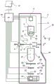
图1(未按比例)是根据本发明实施例的带电粒子显微镜M的实施例的高度的示意图。更具体地说,它示出了透射式显微镜M的实施例,在这种情况下,它是TEM/STEM(例如,尽管在本发明的背景下它可以正如SEM(参见图2)或基于离子的显微镜一样有效)。在图1中,在真空外壳2内,电子源4产生电子束B,该电子束B沿着电子光轴B’传播并穿过电子光学照明器6,用于将电子引导/聚焦到试样S的选定部分(例如,其可以被(局部地)变薄/平面化)。还描绘了致偏器8,其(除了其他事物之外)可用于引起所述束B的扫描移动。Figure 1 (not to scale) is a schematic view of the height of an embodiment of a charged particle microscope M according to an embodiment of the invention. More specifically, it shows an embodiment of a transmission microscope M, which in this case is a TEM/STEM (eg, although in the context of the present invention it can be just as SEM (see Figure 2) or ion-based as effective as a microscope). In Figure 1, within the
试样S被保持在试样夹持器H上,该夹持器H可通过定位装置/台A以多个自由度定位,其移动托架A’,夹持器H(可拆卸地)附加到托架中;例如,试样夹持器H可包括指状物,该指状物(除了其他事物之外)可在X Y平面内移动(见所描绘的笛卡尔坐标系;通常,平行于Z的运动和关于X/Y的倾斜也是可能的)。这样的移动允许试样S的不同部分被沿着轴B’(在Z方向)移动的电子束B照亮/成像/检查(和/或允许进行扫描运动,作为束扫描的替代)。例如,如果需要,可以使可选的冷却装置(未描绘)与试样夹持器H密切热接触,以便将其(以及由此将试样S)维持在低温下。Specimen S is held on specimen holder H, which can be positioned in multiple degrees of freedom by positioning means/stage A, which moves carriage A', holder H (removably) attached into the holder; for example, the specimen holder H may include fingers that (among other things) are movable in the XY plane (see Cartesian coordinate system depicted; typically, parallel to Z movement and tilt with respect to X/Y are also possible). Such movement allows different parts of the specimen S to be illuminated/imaged/inspected by the electron beam B moving along the axis B' (in the Z direction) (and/or allows for a scanning motion as an alternative to beam scanning). For example, if desired, an optional cooling device (not depicted) can be brought into intimate thermal contact with the sample holder H in order to maintain it (and thus the sample S) at a low temperature.
电子束B将与试样S相互作用,如此导致各种类型的“受激”辐射从试样S发射,包括(例如)二次电子、背散射电子、X射线和光辐射(阴极射线致发光)。如果需要,可以借助分析装置22检测这些辐射类型中的一种或多种,例如,其可以是组合的闪烁器/光电倍增器或EDX或EDS(能量色散X射线频谱学)模块;在这种情况下,可以使用与SEM中基本相同的原理来构建图像。然而,可替代地或补充地,可研究穿过(通过)试样S、从试样S中退出/发射、以及沿轴B’继续传播(基本上,尽管通常有一些偏转/散射)的电子。这样的透射电子流量进入成像系统(投影透镜)24,其通常包括各种静电/磁透镜、致偏器、校正器(例如消像散器)等。在正常(非扫描)TEM模式,该成像系统24可以将透射的电子流量聚焦到荧光屏26上,如果需要,其可以缩回/撤回(如由箭头26’示意性所示),以便使其离开轴B’。试样S(的部分)的图像(或衍射图)将由成像系统24在荧光屏26上形成,并且这可以通过位于外壳2的壁的适当部分中的观察端口28进行观察。例如,荧光屏26的缩回机构性质上可以是机械的和/或电气的,并且在此没有描述。The electron beam B will interact with the sample S, thus causing various types of "stimulated" radiation to be emitted from the sample S, including (for example) secondary electrons, backscattered electrons, X-rays, and optical radiation (cathode luminescence) . If desired, one or more of these radiation types can be detected by means of an
作为在荧光屏26上观察图像的替代,可以取而代之地利用这样的事实,即离开成像系统24的电子流量的聚焦深度通常相当大(例如,1米的数量级)。因此,可以在荧光屏26的下游使用各种其他类型的分析设备,例如:Instead of viewing the image on the
-TEM摄像机30。在摄像机30处,例如,电子流量可形成静态图像(或衍射图),该图像可由控制器/处理器20处理并显示在例如平板显示器的显示装置(未描绘)上。当不需要时,可以缩回/撤回摄像机30(如由箭头30’示意性所示),以使其远离轴B’。-
-STEM摄像机32。摄像机32的输出可以记录为试样S上所述束B的(X,Y)扫描位置的函数,并且可以构建图像,该图像是作为X、Y函数的摄像机32的输出的“映射”。摄像机32可以包括直径为例如20 mm的单个像素,与摄像机30中典型地存在的像素矩阵相反。此外,摄像机32通常具有比摄像机30(例如,每秒102个图像)更高的采集速率(例如,每秒106个点)。再次,当不需要时,可以缩回/撤回摄像机32(如由箭头32’示意性所示),以便使其离开轴B’(尽管在例如甜甜圈形状的环形暗场摄像机 32的情况下,这种缩回不是必需的;在这种摄像机中,当摄像机不使用时,中心孔允许流量通过)。-
-作为使用摄像机30或32成像的替代,还可以调用分光设备34,例如,其可以是EELS模块。- Instead of imaging with
应当注意,项目30、32和34的次序/位置并不严格,并且许多可能的变化是可以想象的。例如,分光设备34也可以被集成到成像系统24中。It should be noted that the order/position of
在所示的实施例中,显微镜M还包括可缩回的X射线计算机断层扫描(CT)模块,通常由参考40指示。在计算机断层扫描(也称为断层成像)中,源和(截然相对的)检测器被用于沿不同的视线检查试样,以便从不同的视角采集试样的穿透性的观测数据。In the embodiment shown, the microscope M also includes a retractable X-ray computed tomography (CT) module, generally indicated by
注意,控制器(计算机处理器)20通过控制线(总线)20’连接到所示的各种组件。该控制器20可以提供多种功能,例如同步动作、提供选点、处理信号、执行计算、以及在显示装置(未描绘)上显示消息/信息。不用说,(示意性描绘的)控制器20可以(部分地)在外壳2内部或外部,并且可以根据需要具有单一或复合结构。Note that the controller (computer processor) 20 is connected to the various components shown by control lines (bus) 20'. The
技术人员将理解,外壳2的内部不必保持严格的真空;例如,在所谓的“环境TEM/STEM”中,故意将给定气体的背景气氛引入/维持在外壳2内。技术人员还将理解,在实践中,限制外壳2的体积可能是有利的,以便在可能的情况下,它基本上抱住轴B’,采用小管子(例如,直径为1cm的数量级)的形式,所使用的电子束通过它,但扩大以容纳这样的结构:源4,试样夹持器H,荧光屏26,摄像机30,摄像机32,分光设备34等。The skilled person will understand that the interior of the
根据本发明和图1所示实施例的带电粒子显微镜M因此包括光学柱筒O,包含带电粒子源4、形成透镜的最终探针6和扫描仪8,用于将从所述带电粒子源4发射的带电粒子束B聚焦到试样上。该设备还包括位于所述形成透镜的最终探针6下游的、并被布置成保持所述试样S的试样台A、H。该设备还包括第一检测器22,用于检测源于所述试样的第一类型的发射,所述试样响应从所述带电粒子源4发射的带电粒子B的入射。在所示的实施例中,第一检测器22是分析装置22,如前所述,其可以是组合的闪烁器/光电倍增器或EDS(能量色散X射线频谱学)模块。在优选实施例中,所述第一检测器是EDS。此外,根据本发明的设备包括(借助于线路20’)连接到所述第一检测器22(示意性所示)的控制装置20。根据本发明,所述带电粒子显微镜M被布置成用于执行根据本发明所述的方法,稍后将借助于图3至图6进行解释。The charged particle microscope M according to the invention and the embodiment shown in FIG. 1 thus comprises an optical cylinder O containing a
现在首先参考图2,示出了根据本发明的设备的另一个实施例。图2(未按比例)是根据本发明的带电粒子显微镜M的高度的示意图;更具体地说,它示出了非透射式显微镜M的实施例,在这种情况下,它是SEM(尽管在本发明的背景下,例如,它可以正如基于离子的显微镜一样有效)。在图中,与图1中的项目对应的部件用相同的参考符号指示,并且这里将不单独讨论。除图1外,是(除了其他事物之外)以下部件:Referring now first to Figure 2, another embodiment of an apparatus according to the present invention is shown. Figure 2 (not to scale) is a schematic representation of the height of a charged particle microscope M according to the invention; more specifically, it shows an embodiment of a non-transmission microscope M, in this case a SEM (although In the context of the present invention, for example, it can be as effective as ion-based microscopy). In the figures, components corresponding to items in FIG. 1 are designated with the same reference numerals and will not be discussed separately here. In addition to Figure 1, are (among other things) the following components:
-2a:真空端口,其可打开以将物品(组件,试样)引入/移出真空室2的内部,或例如往其上安装辅助装置/模块。如果需要,显微镜M可以包括多个这样的端口2a;-2a: Vacuum port, which can be opened to introduce/remove items (components, samples) into/out of the interior of the
-10a,10b:照明器6中的示意性描绘的透镜/光学元件;- 10a, 10b: Schematically depicted lenses/optics in
-12:电压源,如果需要,允许试样夹持器H或至少试样S被偏置(浮动)到相对于地的电位;-12: A voltage source that, if required, allows the specimen holder H or at least the specimen S to be biased (floated) to a potential relative to ground;
-14:显示器,如FPD 或CRT;-14: Display such as FPD or CRT;
-22a、22b:分段电子检测器22a,包括设置在中心孔径22b(允许所述束B通过)周围的多个独立检测段(例如象限)。例如,这种检测器可用于研究来自试样S的输出(二次或背散射)电子的流量(的角相关性)。- 22a, 22b: a
因此,如图2所示的带电粒子显微镜M包括光学柱筒O,包含带电粒子源4、形成透镜10a、10b的最终探针6和扫描仪8,用于将从所述带电粒子源4发射的带电粒子束B聚焦到试样S上。该设备还包括试样台A、H,位于所述形成透镜的最终探针6的下游,并被布置成用于保持所述试样S。所述设备还包括第一检测器22,用于检测源于所述试样的第一类型的发射,所述试样响应于从所述带电粒子源4发射的带电粒子B的入射。在所示的实施例中,第一检测器22是所述分析装置22,如前所述,其可以是组合的闪烁器/光电倍增器或EDS(能量色散X射线频谱学)模块。在替代实施例中,第一检测器22可以是分段检测器22a、22b。在优选实施例中,所述第一检测器是EDS。此外,根据本发明的设备包括所述控制装置20,其(借助于线路20’)连接到所述第一检测器22。Thus, a charged particle microscope M as shown in FIG. 2 comprises an optical cylinder O containing a charged
图1和图2所示的设备可用于使用根据本发明的方法检查样品。一般而言,该方法的实施例均包括以下一般步骤:The apparatus shown in Figures 1 and 2 can be used to examine samples using the method according to the present invention. In general, embodiments of the method include the following general steps:
-在所述样品S的至少一部分上扫描所述带电粒子束B;- scanning the charged particle beam B over at least a portion of the sample S;
-使用第一检测器22获得测量的检测器信号,所述检测器信号对应于来自多个采样位置的样品S的第一类型的发射;- using the
-处理所述测量的检测器信号;以及- processing the measured detector signals; and
-以数据表示所述测量的检测器信号。- Data representation of the measured detector signal.
根据本文定义的方法,处理需要若干步骤,借助于图3至图6所示的实施例来说明这些步骤。According to the method defined herein, the processing requires several steps, which are illustrated with the aid of the embodiments shown in FIGS. 3 to 6 .
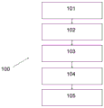
现在参考图3,示出了如本文所述方法的实施例。所述方法100包括提供101数据类元素集的步骤,其中每个数据类元素将期望的检测器22信号与对应样品信息值相关联。所述方法还包括将所述测量的检测器信号与所述数据类元素集(如步骤101中所提供)进行比较102的步骤。然后,在步骤103中,确定至少一个概率,其中所述概率指示所述测量的检测器信号属于所述数据类元素集中的某一个的概率。基于此,将至少一个样品信息值和所述至少一个概率分配104给多个采样位置中的每一个。于是,就可以用对应样品信息值和对应的概率以数据表示105所述多个采样位置。Referring now to FIG. 3, an embodiment of a method as described herein is shown. The
图4示出了数据类元素201-203的集200的示例,其中每个数据类元素201-203将期望的检测器信号211-213与对应的样品值信息值221-223相关联。在所示的示例中,使用了总共三个数据类元素201-203,但是需要注意的是,原则上可以使用任意数量的数据类元素。当只对某些数据值感兴趣时,有限数量的数据类元素是有用的,而其他数据值可以被分类为“其他”。数据类元素的有限集加快了数据处理。Figure 4 shows an example of a
在图4所示的示例中,数据类元素201-203被用于将期望的频谱211-213与用于表示物质A-C的数据值221-223相关联。数据类元素201将特定频谱211与数据值221的“物质A”相关联,数据类元素202将另一频谱212与数据值222的“物质B”相关联,以及数据类元素203将另外的频谱213与数据值223的“物质C”相关联。In the example shown in Figure 4, data class elements 201-203 are used to associate desired frequency spectra 211-213 with data values 221-223 representing substances A-C.
在执行该方法期间,当对样品进行研究时,将获得检测器信号。检测器信号可以被编码成频谱,并且该频谱可以与数据类元素201-203进行比较。可以想象的是,测量的频谱与一个或多个预定义的数据类元素201-203有一些相似性。例如,测量的频谱可以是20%相似于频谱211,10%相似于频谱212,以及70%相似于频谱213。这种相似性评分已经给出这样的指示,即测量的频谱属于“物质C”的数据值223是可能的。然后,将该数据值和对应的概率(其可以等于70%的相似性评分,或者可以是基于进一步计算的另一个值)分配给各自的采样位置。因此,这里将样品信息值(测量的位置包括物质C)及其概率分配给各自的采样位置,并且可以通过将其存储在数据存储器中或通过将其显示给用户来以数据表示。During the execution of the method, a detector signal will be obtained when the sample is studied. The detector signal can be encoded into a spectrum, and the spectrum can be compared to the data class elements 201-203. It is conceivable that the measured spectrum has some similarity to one or more predefined data class elements 201-203. For example, the measured spectrum may be 20% similar to
图5示出了结合本文所述方法的算法301的实施例的流程图300,其中特别提供彩色图像作为以数据的表示。在图5中,输入数据311,特别是测量的检测器信号或处理的检测器信号(例如频谱),被提供为算法301的输入。在步骤312中,概率分类器处理数据以确定似然(likelihoods)。在步骤313中,使用贝叶斯算子。贝叶斯算子推断在步骤312中处理的输入数据311实际上属于在数据类元素集中定义的个别类中的一个或多个的概率(参见图4)。这样,在步骤314中,可以定义使用颜色特性的表示。然后,可以给出最终数据表示315作为输出数据。例如,这可以是彩色图像。该算法还包括在步骤312-314中使用的若干参数320,并且这些参数可以是静态和/或动态的。例如,这些参数可以包括内置的机器学习方法,这些方法利用每个传入数据点进行学习,并自动推断数据类元素的定义,其减少用户必须经历的步骤的数量。FIG. 5 shows a
图5所示的实施例使用概率分类器312、贝叶斯算子313和颜色混合步骤314。概率分类器针对预定义的或算法确定的类的集,计算每个输入数据点的相似性。这些类可以人工(由用户)定义,或者自动(通过机器学习)定义。给定单个数据点,分类器计算每个类的似然。类的更高的似然意味着数据点更可能属于该类。概率分类器可以被简化为“硬分类器”,其例如通过选择最高似然给每个数据点精确地分配一个类,在这种情况下,提供“默认”类以容纳未被任何其他类覆盖的数据。我们提出了适合各种模式和应用的概率分类器的各种实现。在EDS中,可以使用基于模糊逻辑规则的分类器(人工分类)、使用应用于化学定量数据的高斯混合模型的分类器和应用于稀疏EDS谱的潜在狄利克雷分配(LDA)分类器。The embodiment shown in FIG. 5 uses a
作为示例,在EDS中,测量的频谱311(例如显示90%的硅和10%的氧)被输入到算法中。提供数据类,例如C1对应于硅(Si)以及C2对应于SixOx。因此,数据类可以对应于化学元素,也可以对应于成分。在步骤312中,对测量的频谱进行分析,并将数据值(例如,Si,SixOx)和一些概率被附加到其上。基于这些概率,贝叶斯算子可以进一步处理该数据,并得出这样的结论:给定数据,化学分布的概率为:98%的Si和2%的SixOx。因此,在这种情况下,最可能的是测量的频谱实际上属于硅。然而,为了输出概率,可以在步骤314中使用颜色混合以供输出彩色图像。颜色混合可以包括以与确定的概率相对应的量混合颜色色调,并且输出可以包括单一(混合的)颜色色调。As an example, in EDS, a measured spectrum 311 (eg showing 90% silicon and 10% oxygen) is input into the algorithm. Data classes are provided, eg C1 corresponds to silicon (Si ) and C2 corresponds to SixOx . Thus, data classes can correspond to chemical elements as well as compositions. In
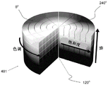
图6示出了可用于以所获得的结果的数据的表示。HSV彩色空间101是这样的彩色空间,其使用色调(通常称为“颜色”,例如红色、绿色、蓝色)、饱和度(通常称为颜色的强度或纯度)和值(通常称为颜色的明暗度)来描述具体颜色的属性。HSV彩色空间可以用如图3所示的圆柱形几何结构来表示,其中色调,它的角度大小,从0°处的红基色开始,在120°处通过绿基色,以及在240°处通过蓝基色,然后在360°处绕回来到红色。中心垂直轴包括中性、无色或灰色,范围从0值处的黑色(图3的底部)到1值处的白色(图3的顶部)。随着半径的增加,即从中心向外,颜色的饱和度增加。HSV彩色空间的细节本身为彩色空间领域技术人员所知。Figure 6 shows a representation of the data that can be used to obtain the results.
现在参考回图4和图5,可以想象的是某些色调与某些数据类元素201-203相关联。例如,颜色色调红色可以与数据类元素201相关联,以及颜色色调蓝色可以与数据类元素202相关联。如果图5的算法指示化学分布的概率为约90%的“物质A”和约10%的“物质B”,则可以例如以90-10的比率混合这些颜色色调,并输出到最终的图像表示中。这样,用户可以看到该物质很可能是“物质A”,因为所使用的颜色色调与红色相像,但用户也看到,并不是100%确定它实际上是“物质A”。Referring now back to Figures 4 and 5, it is conceivable that certain hues are associated with certain data class elements 201-203. For example, the color tint red may be associated with
本文所描述的方法的实施例提供了一种通用算法框架,用于将多模标量或频谱数据(例如EDS频谱、光致发光等)转换为随后可与灰度图像混合的颜色。这里提出的框架可以基于概率分类器312,该分类器定义许多数据类元素(例如,不同的元素或相),并将先验概率(权重)和颜色分配给每个数据类元素,随后使用贝叶斯数学对其进行处理。Embodiments of the methods described herein provide a general algorithmic framework for converting multimodal scalar or spectral data (eg, EDS spectra, photoluminescence, etc.) into colors that can then be mixed with grayscale images. The framework proposed here can be based on a
本文描述了本发明的实施例。所需的保护由所附权利要求授予。Embodiments of the invention are described herein. The required protection is afforded by the appended claims.
Claims (13)
Applications Claiming Priority (2)
| Application Number | Priority Date | Filing Date | Title |
|---|---|---|---|
| EP19172810.4A EP3736849A1 (en) | 2019-05-06 | 2019-05-06 | Method of examining a sample using a charged particle microscope |
| EP19172810.4 | 2019-05-06 |
Publications (3)
| Publication Number | Publication Date |
|---|---|
| CN111982938A true CN111982938A (en) | 2020-11-24 |
| CN111982938B CN111982938B (en) | 2024-06-04 |
| CN111982938B9 CN111982938B9 (en) | 2024-07-02 |
Family
ID=66429293
Family Applications (1)
| Application Number | Title | Priority Date | Filing Date |
|---|---|---|---|
| CN202010362647.4A Active CN111982938B9 (en) | 2019-05-06 | 2020-04-30 | Method for examining samples using a charged particle microscope |
Country Status (5)
| Country | Link |
|---|---|
| US (1) | US11327032B2 (en) |
| EP (1) | EP3736849A1 (en) |
| JP (1) | JP7516098B2 (en) |
| KR (1) | KR102841023B1 (en) |
| CN (1) | CN111982938B9 (en) |
Families Citing this family (6)
| Publication number | Priority date | Publication date | Assignee | Title |
|---|---|---|---|---|
| EP3736562A1 (en) * | 2019-05-06 | 2020-11-11 | FEI Company | Method of examining a sample using a charged particle microscope |
| US11114274B2 (en) * | 2019-12-23 | 2021-09-07 | Carl Zeiss Smt Gmbh | Method and system for testing an integrated circuit |
| US11373839B1 (en) * | 2021-02-03 | 2022-06-28 | Fei Company | Method and system for component analysis of spectral data |
| WO2022266269A1 (en) * | 2021-06-15 | 2022-12-22 | Own Christopher Su Yan | Sample delivery, data acquisition, and analysis, and automation thereof, in charged-particle-beam microscopy |
| US11703468B2 (en) | 2021-07-01 | 2023-07-18 | Fei Company | Method and system for determining sample composition from spectral data |
| US20240153735A1 (en) | 2022-11-09 | 2024-05-09 | Fei Company | Pixel elements, particle beam microscopes including the same, and associated methods |
Citations (5)
| Publication number | Priority date | Publication date | Assignee | Title |
|---|---|---|---|---|
| AU2012200707A1 (en) * | 2003-03-28 | 2012-03-01 | Inguran, Llc | "Photo-damage apparatus and methods for sorting particles" |
| US20140019443A1 (en) * | 2012-07-10 | 2014-01-16 | Venor, Inc. | Systems and methods for discovering content of predicted interest to a user |
| US20140035943A1 (en) * | 2011-02-15 | 2014-02-06 | Oxford Instruments Nanotechnology Tools Limited | Material identification using multiple images |
| US20140117229A1 (en) * | 2012-10-26 | 2014-05-01 | Fei Company | Mineral identification using sequential decomposition into elements from mineral definitions |
| US20170115241A1 (en) * | 2015-10-21 | 2017-04-27 | Trustees Of Princeton University | Transition edge sensor for x-ray fluorescence (tes-xrf) for high resolution material identification |
Family Cites Families (11)
| Publication number | Priority date | Publication date | Assignee | Title |
|---|---|---|---|---|
| JP2004151045A (en) * | 2002-11-01 | 2004-05-27 | Hitachi High-Technologies Corp | Electron microscope or X-ray analyzer and sample analysis method |
| EP2047245B1 (en) * | 2006-07-27 | 2022-09-21 | Thermo Electron Scientific Instruments LLC | Automatic material labeling during spectral image data acquisition |
| EP2525385A1 (en) * | 2011-05-16 | 2012-11-21 | Fei Company | Charged-particle microscope |
| EP2835817B1 (en) * | 2013-08-09 | 2017-12-20 | Carl Zeiss Microscopy Ltd. | Method for semi-automated particle analysis using a charged particle beam |
| US9714908B2 (en) * | 2013-11-06 | 2017-07-25 | Fei Company | Sub-pixel analysis and display of fine grained mineral samples |
| US9183656B2 (en) * | 2014-03-11 | 2015-11-10 | Fei Company | Blend modes for mineralogy images |
| EP2998979A1 (en) * | 2014-09-22 | 2016-03-23 | Fei Company | Improved spectroscopy in a transmission charged-particle microscope |
| EP3040714A1 (en) * | 2014-12-30 | 2016-07-06 | Fei Company | Charged Particle Microscope with improved spectroscopic functionality |
| KR102194154B1 (en) * | 2016-09-01 | 2020-12-22 | 주식회사 히타치하이테크 | Pattern measurement device and computer program |
| WO2018152202A1 (en) * | 2017-02-14 | 2018-08-23 | Massachusetts Institute Of Technology | Systems and methods for automated microscopy |
| US9905394B1 (en) * | 2017-02-16 | 2018-02-27 | Carl Zeiss Microscopy Gmbh | Method for analyzing an object and a charged particle beam device for carrying out this method |
-
2019
- 2019-05-06 EP EP19172810.4A patent/EP3736849A1/en active Pending
-
2020
- 2020-04-30 CN CN202010362647.4A patent/CN111982938B9/en active Active
- 2020-05-01 JP JP2020081299A patent/JP7516098B2/en active Active
- 2020-05-04 KR KR1020200053087A patent/KR102841023B1/en active Active
- 2020-05-06 US US16/867,972 patent/US11327032B2/en active Active
Patent Citations (6)
| Publication number | Priority date | Publication date | Assignee | Title |
|---|---|---|---|---|
| AU2012200707A1 (en) * | 2003-03-28 | 2012-03-01 | Inguran, Llc | "Photo-damage apparatus and methods for sorting particles" |
| US20140035943A1 (en) * | 2011-02-15 | 2014-02-06 | Oxford Instruments Nanotechnology Tools Limited | Material identification using multiple images |
| US20140019443A1 (en) * | 2012-07-10 | 2014-01-16 | Venor, Inc. | Systems and methods for discovering content of predicted interest to a user |
| US20140117229A1 (en) * | 2012-10-26 | 2014-05-01 | Fei Company | Mineral identification using sequential decomposition into elements from mineral definitions |
| US20150338358A1 (en) * | 2012-10-26 | 2015-11-26 | FFI Company | Mineral Identification Using Sequential Decomposition into Elements from Mineral Definitions |
| US20170115241A1 (en) * | 2015-10-21 | 2017-04-27 | Trustees Of Princeton University | Transition edge sensor for x-ray fluorescence (tes-xrf) for high resolution material identification |
Non-Patent Citations (2)
| Title |
|---|
| NELLY R. HAJIZADEH ET AL: "Consensus Bayesian assessment of protein molecular mass from solution X-ray scattering data", 《SCIENTIFICREPORTS》, pages 1 - 13 * |
| 邬小平 等: "基于贝叶斯决策的双能X射线材料分辨算法研究", 《中国体视学与图像分》, pages 162 - 165 * |
Also Published As
| Publication number | Publication date |
|---|---|
| CN111982938B9 (en) | 2024-07-02 |
| JP7516098B2 (en) | 2024-07-16 |
| EP3736849A1 (en) | 2020-11-11 |
| CN111982938B (en) | 2024-06-04 |
| KR20200130142A (en) | 2020-11-18 |
| US20200363349A1 (en) | 2020-11-19 |
| JP2020184539A (en) | 2020-11-12 |
| US11327032B2 (en) | 2022-05-10 |
| KR102841023B1 (en) | 2025-07-31 |
Similar Documents
| Publication | Publication Date | Title |
|---|---|---|
| CN111982938B (en) | Method for examining a sample using a charged particle microscope | |
| CN110849926B (en) | Method for examining samples using a charged particle microscope | |
| JP7592955B2 (en) | How to Examine a Sample Using a Charged Particle Microscope | |
| JP7608695B2 (en) | How to Examine a Sample Using a Charged Particle Microscope | |
| US11971372B2 (en) | Method of examining a sample using a charged particle microscope | |
| JP7608696B2 (en) | Method for examining a sample using a charged particle microscope to obtain an electron energy loss spectroscopy (EELS) spectrum | |
| US20240027377A1 (en) | Method of examining a sample using a charged particle microscope |
Legal Events
| Date | Code | Title | Description |
|---|---|---|---|
| PB01 | Publication | ||
| PB01 | Publication | ||
| SE01 | Entry into force of request for substantive examination | ||
| SE01 | Entry into force of request for substantive examination | ||
| GR01 | Patent grant | ||
| GR01 | Patent grant | ||
| CI03 | Correction of invention patent |
Correction item: Claims Correct: Claims 1-13 submitted on April 25, 2024 False: Claims 1-13 submitted on April 25, 2024 and amended by the examiner in accordance with their authority Number: 23-01 Page: ?? Volume: 40 |