CN111982945A - Method and application of time-resolved dark field image acquisition based on ultrafast transmission electron microscope system - Google Patents
Method and application of time-resolved dark field image acquisition based on ultrafast transmission electron microscope system Download PDFInfo
- Publication number
- CN111982945A CN111982945A CN201910438469.6A CN201910438469A CN111982945A CN 111982945 A CN111982945 A CN 111982945A CN 201910438469 A CN201910438469 A CN 201910438469A CN 111982945 A CN111982945 A CN 111982945A
- Authority
- CN
- China
- Prior art keywords
- image
- sample
- sub
- diffraction
- dark field
- Prior art date
- Legal status (The legal status is an assumption and is not a legal conclusion. Google has not performed a legal analysis and makes no representation as to the accuracy of the status listed.)
- Granted
Links
Images





Classifications
-
- G—PHYSICS
- G01—MEASURING; TESTING
- G01N—INVESTIGATING OR ANALYSING MATERIALS BY DETERMINING THEIR CHEMICAL OR PHYSICAL PROPERTIES
- G01N23/00—Investigating or analysing materials by the use of wave or particle radiation, e.g. X-rays or neutrons, not covered by groups G01N3/00 – G01N17/00, G01N21/00 or G01N22/00
- G01N23/20—Investigating or analysing materials by the use of wave or particle radiation, e.g. X-rays or neutrons, not covered by groups G01N3/00 – G01N17/00, G01N21/00 or G01N22/00 by using diffraction of the radiation by the materials, e.g. for investigating crystal structure; by using scattering of the radiation by the materials, e.g. for investigating non-crystalline materials; by using reflection of the radiation by the materials
- G01N23/20058—Measuring diffraction of electrons, e.g. low energy electron diffraction [LEED] method or reflection high energy electron diffraction [RHEED] method
Landscapes
- Chemical & Material Sciences (AREA)
- Crystallography & Structural Chemistry (AREA)
- Physics & Mathematics (AREA)
- Health & Medical Sciences (AREA)
- Life Sciences & Earth Sciences (AREA)
- Analytical Chemistry (AREA)
- Biochemistry (AREA)
- General Health & Medical Sciences (AREA)
- General Physics & Mathematics (AREA)
- Immunology (AREA)
- Pathology (AREA)
- Analysing Materials By The Use Of Radiation (AREA)
Abstract
一种基于超快透射电镜系统获取高衬度超快时间分辨暗场像的方法及应用。通过采用高汇聚角入射束成像,采用大尺寸物镜光阑,以衍射电子作为信号进行成像,获得超快尺度下的时间分辨暗场像,相对于超快透射电镜明场像,具有相反衬度的暗场像减少了背底信号,由于高汇聚角和大尺寸物镜光阑的结合使用,并通过双束衍射、暗场像的优化调节,从而提高采集信号的信噪比,相对于衍射模式信号能更直接地观察样品内部不同区域的变化过程,具有高空间分辨率,拓展了超快电镜暗场方式表征样品的范围,可以分析纳米颗粒受激光激发后的衬度变化细节,并且能应用于超快时间尺度内材料不同晶格取向的点阵结构弛豫和共振动力学过程的表征分析。

A method and application for obtaining a high-contrast ultrafast time-resolved dark field image based on an ultrafast transmission electron microscope system. By using a high-convergence angle incident beam imaging, using a large-size objective lens aperture, and imaging with diffracted electrons as a signal, a time-resolved dark-field image at an ultrafast scale is obtained. Compared with the ultrafast TEM bright-field image, it has opposite contrast. The dark field image reduces the background signal. Due to the combination of the high convergence angle and the large-size objective diaphragm, and through the optimal adjustment of double-beam diffraction and dark field image, the signal-to-noise ratio of the collected signal is improved, compared with the diffraction mode. The signal can more directly observe the change process of different regions inside the sample, has high spatial resolution, expands the scope of the ultrafast electron microscope dark field method to characterize the sample, can analyze the details of the contrast change of the nanoparticles after being excited by the laser, and can be applied Characterization of lattice relaxation and resonance dynamics in materials with different lattice orientations on ultrafast timescales.
Description
技术领域technical field
本公开属于电子显微学的暗场表征以及超快电子显微镜技术领域,涉及一种基于超快透射电镜系统获取时间分辨暗场像的方法及应用,特别是一种基于超快透射电镜系统获取高衬度超快时间分辨暗场像的方法及应用。The present disclosure belongs to the technical field of dark field characterization of electron microscopy and ultrafast electron microscopy, and relates to a method and application for obtaining a time-resolved dark field image based on an ultrafast transmission electron microscope system, in particular to a method for obtaining a time-resolved dark field image based on an ultrafast transmission electron microscope system. Methods and applications for high-contrast ultrafast time-resolved dark field images.
背景技术Background technique
透射电子显微镜是重要的材料表征工具,透射电镜技术经过快速发展,目前空间分辨率已经达到亚埃量级,已经极大满足了实验需求,通过透射电镜表征材料的变化过程成为目前重要发展趋势,例如原位透射电镜以及4D超快透射电镜等。Transmission electron microscopy is an important material characterization tool. After rapid development of transmission electron microscopy technology, the spatial resolution has reached the sub-angstrom level, which has greatly satisfied the experimental needs. Characterizing the change process of materials by transmission electron microscopy has become an important development trend at present. Such as in situ transmission electron microscopy and 4D ultrafast transmission electron microscopy.
超快透射电镜是与超快光学手段相结合,具备了透射电镜高空间分辨与超快光学高时间分辨的优点,并且突破了电荷耦合器件(CCD)相机采集速度的限制,实现了飞秒至微秒范围内材料结构动力学变化过程,从而揭示物理或化学过程中原子尺度的变化。超快透射电镜至今已发展了多种表征技术,可根据图像或者衍射信息,或者结合电子能量损失谱(EELS)来分析材料的等离子体效应。Ultrafast transmission electron microscopy is combined with ultrafast optical means, which has the advantages of high spatial resolution of transmission electron microscopy and high time resolution of ultrafast optics, and breaks through the limitation of the acquisition speed of charge-coupled device (CCD) cameras, realizing femtosecond to The dynamics of material structure changes in the microsecond range, thereby revealing atomic-scale changes in physical or chemical processes. Ultrafast transmission electron microscopy has developed a variety of characterization techniques to analyze the plasmonic effects of materials based on image or diffraction information, or in combination with electron energy loss spectroscopy (EELS).
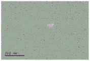
目前基于超快透射电镜数据采集以明场像和衍射斑点为主,研究材料受脉冲激光激发后内部的动力学变化过程,2018年,有的研究基于超快透射电镜明场像,通过金颗粒衬度的变化,研究了等离子金纳米颗粒内部以及颗粒之间受泵浦产生的晶格振动过程,但是由于明场像下主要是透射电子,晶格变化导致明场像衬度变化的信号,相对于透射电子信号只占一小部分,因此存在衬度变化不明显的问题,同时超快透射电镜中成像电子数量低于常规透射电镜,因此得到的结果信噪比比较差,最终得到图像并不能明显揭示激光激发后样品的晶格变化过程,光电子模式下以较大电子束斑和最小尺寸物镜光阑拍摄得到的明场像图谱如图1所示。At present, based on ultrafast TEM data acquisition, bright field images and diffraction spots are mainly used to study the internal dynamic changes of materials after being excited by pulsed lasers. In 2018, some studies were based on ultrafast TEM bright field images. Contrast change, the lattice vibration process generated by pumping inside the plasmonic gold nanoparticles and between the particles is studied, but because the bright field image is mainly transmitted electrons, the lattice change leads to the signal of the contrast change of the bright field image, Compared with the transmission electron signal, it only accounts for a small part, so there is a problem that the contrast change is not obvious. At the same time, the number of imaging electrons in the ultrafast transmission electron microscope is lower than that of the conventional transmission electron microscope, so the signal-to-noise ratio of the result obtained is relatively poor, and the final image is The lattice change process of the sample after laser excitation cannot be clearly revealed. The bright-field image pattern captured by the larger electron beam spot and the smallest size of the objective lens in the optoelectronic mode is shown in Figure 1.
在暗场像中,采用衍射电子进行成像,与明场像相比较衬度相反,样品区域成为亮区,衬底区域成为暗区,背景信号减弱,样品信号强度的变化更加明显,信噪比相对于明场像得到了极大地提高,相对于超快系统明场像,可以更直观表示出样品在超快过程中变化。In the dark field image, diffracted electrons are used for imaging. Compared with the bright field image, the contrast is opposite, the sample area becomes a bright area, the substrate area becomes a dark area, the background signal is weakened, the change of the sample signal intensity is more obvious, and the signal-to-noise ratio is Compared with the bright field image, it has been greatly improved, and compared with the bright field image of the ultrafast system, it can more intuitively represent the change of the sample in the ultrafast process.
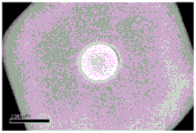
在常规透射电镜中,拍摄暗场像往往要求电子束以近似平行状态照射于样品上,汇聚角比较小,从而可以利用最小尺寸的物镜光阑拍摄暗场像,保证衍射电子透过,并阻挡绝大部分(非弹性)散射电子,但是这些方式并不能直接应用于超快透射电镜中。由于超快透射电镜中,电子以脉冲形式被激光脉冲激发,产生电子数量远少于常规电镜,因此得到暗场像衬度非常差,光电子模式下以较大电子束斑和最小尺寸物镜光阑拍摄得到的暗场像图谱如图2所示。In conventional transmission electron microscopes, the shooting of dark field images often requires the electron beam to be irradiated on the sample in an approximately parallel state, and the convergence angle is relatively small, so that the dark field image can be shot with the smallest size of the objective lens to ensure that the diffracted electrons pass through and block the Most of the electrons are scattered (inelastically), but these methods are not directly applicable to ultrafast transmission electron microscopy. In ultrafast transmission electron microscopy, electrons are excited by laser pulses in the form of pulses, and the number of electrons generated is much less than that of conventional electron microscopy, so the dark field image contrast is very poor, and in optoelectronic mode, a larger electron beam spot and the smallest size of the objective lens aperture are used. The dark field image spectrum obtained by shooting is shown in Figure 2.
目前基于超快透射电镜的暗场像模式工作基于观测样品的机械运动为主,而且基于暗场像的工作应用范围较小,对于样品的选择存在较大的限制,无法应用小尺寸样品,例如纳米颗粒等样品的表征。此外,现有的极少数的研究中采用暗场像表征大尺寸样品得到的图像衬度较差,得到的暗场像未详细分析时间分辨暗场图像本身的强度变化过程,不能明显反应出衬度的变化过程,无法应用于精确的动力学分析。因此尚需一种能够直观并且具备高信噪比的方式来分析样品在超快时间尺度内的动力学变化过程。At present, the dark-field image mode based on ultrafast transmission electron microscopy is mainly based on the mechanical motion of the observed sample, and the application range of the work based on dark-field images is small, and there are great restrictions on the selection of samples, and small-sized samples cannot be applied, such as Characterization of samples such as nanoparticles. In addition, there are very few existing studies that use dark field images to characterize large-size samples, and the image contrast obtained is poor. The degree of change process cannot be applied to accurate kinetic analysis. Therefore, there is still a need for an intuitive and high signal-to-noise method to analyze the dynamic changes of samples on ultrafast time scales.
发明内容SUMMARY OF THE INVENTION
(一)要解决的技术问题(1) Technical problems to be solved
本公开提供了一种基于超快透射电镜系统获取时间分辨暗场像的方法及应用,以至少部分解决以上所提出的技术问题。The present disclosure provides a method and application for obtaining a time-resolved dark field image based on an ultrafast transmission electron microscope system, so as to at least partially solve the above-mentioned technical problems.
(二)技术方案(2) Technical solutions
根据本公开的一个方面,提供了一种基于超快透射电镜系统获取时间分辨暗场像的方法,包括:步骤S12:在热电子模式下,调节得到样品的近似双束衍射以及通过采用一物镜光阑套住衍射斑得到暗场像;步骤S13:在光电子模式下,以较大汇聚角汇聚电子束斑,在衍射模式下获得样品的汇聚束衍射;暗场模式下基于热电子模式的入射电子束倾转角度,采用该物镜光阑选择衍射斑点,得到样品在光电子模式下的时间分辨暗场像,其中该较大汇聚角使得光电子模式下的衍射斑面积大于热电子模式的衍射斑面积。According to an aspect of the present disclosure, there is provided a method for obtaining a time-resolved dark field image based on an ultrafast transmission electron microscope system, comprising: step S12: in the thermionic mode, adjusting to obtain approximate double-beam diffraction of the sample and adopting an objective lens The diaphragm covers the diffraction spot to obtain a dark field image; Step S13: in the photoelectron mode, the electron beam spot is converged at a larger convergence angle, and the focused beam diffraction of the sample is obtained in the diffraction mode; in the dark field mode, the incident based on the thermionic mode The tilt angle of the electron beam, using the objective diaphragm to select the diffraction spot, obtains the time-resolved dark field image of the sample in the photoelectron mode, where the larger convergence angle makes the diffraction spot area in the photoelectron mode larger than that in the thermionic mode .
其中,物镜光阑为大尺寸物镜光阑,该大尺寸物镜光阑的光阑孔径介于10微米至100微米之间;优选介于20微米至40微米之间。Wherein, the objective lens diaphragm is a large-sized objective lens diaphragm, and the diaphragm aperture of the large-sized objective lens diaphragm is between 10 μm and 100 μm; preferably between 20 μm and 40 μm.
其中,在步骤S12之前还包括:步骤S11:在超快透射电镜系统中,调节泵浦激光聚焦位置使其聚焦于样品位置,探测激光聚焦于灯丝产生探测电子脉冲。Wherein, before step S12, it further includes: step S11: in the ultrafast transmission electron microscope system, adjust the focus position of the pump laser to focus on the sample position, and focus the detection laser on the filament to generate detection electron pulses.
在一些实施例中,步骤S11包括:在泵浦激光进入透射电镜系统样品室之前,添加可见光反射镜将泵浦激光反射至光束分析仪上,调节光束分析仪位置找到泵浦激光聚焦位置与聚焦光斑大小,获得聚焦点与聚焦透镜实际距离及聚焦斑点大小;根据聚焦位置,通过三维位移台调节泵浦光路中聚焦透镜位置;在超快透射电镜中放入碳膜,采用最小能量泵浦光激发碳膜位置,实现泵浦激光激发位置与光生探测电子位置重合;以及精细调节聚焦透镜位置,找到最佳聚焦位置。In some embodiments, step S11 includes: before the pump laser enters the sample chamber of the TEM system, adding a visible light mirror to reflect the pump laser to the beam analyzer, and adjusting the position of the beam analyzer to find the pump laser focus position and focus According to the size of the spot, the actual distance between the focus point and the focus lens and the size of the focus spot are obtained; according to the focus position, the position of the focus lens in the pump light path is adjusted by the three-dimensional displacement stage; the carbon film is placed in the ultrafast transmission electron microscope, and the minimum energy pump light is used Excite the position of the carbon film to achieve the coincidence of the excitation position of the pump laser with the position of the photogenerated detection electrons; and finely adjust the position of the focusing lens to find the best focusing position.
在一些实施例中,步骤S13之后还包括:步骤S14:采用自动采集模块采集图像,所述自动采集模块通过软件、或者硬件、或者硬件软件结合方式实现其功能。步骤S14可通过控制一维电动位移台与透射电镜系统成像装置对时间分辨暗场图像进行自动采集与保存;或者通过控制泵浦激光光路中机械快门开关控制泵浦激光,采集参考图像与激发图像。In some embodiments, after step S13, it further includes: step S14: using an automatic acquisition module to acquire images, the automatic acquisition module realizes its function through software, or hardware, or a combination of hardware and software. In step S14, the time-resolved dark field image can be automatically collected and saved by controlling the one-dimensional electric displacement stage and the imaging device of the transmission electron microscope system; or the pump laser can be controlled by controlling the mechanical shutter switch in the pump laser light path, and the reference image and the excitation image can be collected. .
在一些实施例中,步骤S14之后还包括:对采集的图像进行批处理。In some embodiments, after step S14, the method further includes: batch processing the collected images.
在一些实施例中,对采集的图像进行批处理,包括:图像平均化作为参考图像、图像偏移校准、图像强度分析及结果输出等中的一个或多个;其中图像强度分析包括:单像素强度分析、区域强度分析、线强度分析中的一个或多个;其中结果输出包括:图像噪声处理输出、强度曲线输出、位置校准输出、图像互相关值输出、图像漂移量输出、傅里叶分析输出及视频输出中的一个或多个。In some embodiments, the batch processing of the collected images includes one or more of image averaging as a reference image, image offset calibration, image intensity analysis, and result output, etc.; wherein the image intensity analysis includes: a single pixel One or more of intensity analysis, area intensity analysis, and line intensity analysis; wherein the result output includes: image noise processing output, intensity curve output, position calibration output, image cross-correlation value output, image drift amount output, Fourier analysis One or more of output and video output.
根据本公开的另一个方面,还提供了一种采用本公开所述的方法所获取的时间分辨暗场像在分析纳米颗粒受激光激发后的衬度变化细节,以及超快时间尺度内表征不同材料晶格取向的点阵结构弛豫和共振动力学过程的应用。According to another aspect of the present disclosure, there is also provided a time-resolved dark field image obtained by the method described in the present disclosure for analyzing the details of the contrast change of the nanoparticle after being excited by the laser, and characterizing the difference in the ultrafast time scale. Application of lattice relaxation and resonance dynamics processes to lattice orientation of materials.
(三)有益效果(3) Beneficial effects
从上述技术方案可以看出,本公开提供的基于超快透射电镜系统获取时间分辨暗场像的方法及应用,具有以下有益效果:As can be seen from the above technical solutions, the method and application for obtaining a time-resolved dark field image based on an ultrafast transmission electron microscope system provided by the present disclosure have the following beneficial effects:
1、通过采用高汇聚角入射束成像,采用大尺寸物镜光阑,以衍射电子作为信号进行成像,获得超快尺度下的时间分辨暗场像,相对于超快透射电镜明场像,具有相反衬度暗场像减少了背底信号,由于高汇聚角和大尺寸物镜光阑的结合使用,并通过双束衍射、暗场像的优化调节,从而提高采集信号的信噪比,相对于衍射模式信号可以更加直接地观察样品内部不同区域的变化过程,具有高空间分辨率,拓展了超快电镜暗场方式表征样品的范围,可以分析颗粒受激光激发后的衬度变化细节。本公开得到的时间分辨暗场像衬度更高,晶格变化更加明显,可以观测样品在超快时间尺度内的动力学变化过程,例如皮秒,纳秒,或微秒等,同时本公开中包含电子与声子相互作用信息和晶格方向倾转信息,也包含了热散射电子,可用于热散射电子信号分析。1. By using a high-convergence angle incident beam imaging, using a large-size objective lens aperture, and imaging with diffracted electrons as a signal, a time-resolved dark-field image at an ultrafast scale can be obtained. Compared with the ultrafast transmission electron microscope bright-field image, it has the opposite The contrast dark field image reduces the background signal. Due to the combination of the high convergence angle and the large size of the objective lens, and through the optimal adjustment of double beam diffraction and dark field image, the signal-to-noise ratio of the collected signal is improved. Compared with diffraction The mode signal can more directly observe the change process of different regions inside the sample, has high spatial resolution, expands the scope of the ultrafast electron microscope dark field method to characterize the sample, and can analyze the details of the contrast change of the particles after being excited by the laser. The time-resolved dark field image obtained by the present disclosure has higher contrast and more obvious lattice changes, and can observe the dynamic change process of the sample in ultrafast time scales, such as picoseconds, nanoseconds, or microseconds. It contains the interaction information of electrons and phonons and the tilting information of the lattice direction, as well as the heat scattering electrons, which can be used for the analysis of heat scattering electron signals.
2、本公开的图像采集过程采用自动采集,可选择不同的参考模式,并保证采集过程降低外界干扰,并提高采集效率。2. The image acquisition process of the present disclosure adopts automatic acquisition, and different reference modes can be selected to ensure that the acquisition process reduces external interference and improves acquisition efficiency.
3、本公开还提出了对应的数据处理和分析程序,可批量分析采集的数据图像,对样品位置进行漂移校正,对图像进行除噪声和滤波处理,输出单像素强度分析,区域像素强度分析,线强度分析,输出视频等。3. The present disclosure also proposes a corresponding data processing and analysis program, which can analyze the collected data images in batches, perform drift correction on the sample position, perform noise removal and filtering processing on the image, output single pixel intensity analysis, regional pixel intensity analysis, Line strength analysis, output video, etc.
附图说明Description of drawings
图1为已有技术中光电子模式下以较大电子束斑和最小尺寸物镜光阑拍摄得到的明场像图谱。Fig. 1 is a bright-field image spectrum obtained by taking a larger electron beam spot and a minimum size objective lens aperture in the optoelectronic mode in the prior art.
图2为已有技术中光电子模式下以较大电子束斑和最小尺寸物镜光阑拍摄得到的暗场像图谱。FIG. 2 is a dark field image pattern obtained by taking a larger electron beam spot and a minimum size objective lens aperture in the optoelectronic mode in the prior art.
图3为根据本公开一实施例所示的超快透射电镜系统的结构示意图。3 is a schematic structural diagram of an ultrafast transmission electron microscope system according to an embodiment of the present disclosure.
图4为基于本公开的方法采用高汇聚角和大尺寸物镜光阑拍摄得到的暗场像图谱。FIG. 4 is a dark field image map obtained by using a high convergence angle and a large-sized objective lens aperture based on the method of the present disclosure.
图5为根据本公开一实施例所示的基于超快透射电镜系统获取时间分辨暗场像的方法流程图。5 is a flowchart of a method for acquiring a time-resolved dark field image based on an ultrafast transmission electron microscope system according to an embodiment of the present disclosure.
图6A-图6C为根据本公开一实施例所示的根据碳膜烧蚀区域确定焦点位置的示意图。6A-6C are schematic diagrams of determining a focus position according to a carbon film ablation area according to an embodiment of the present disclosure.
图7A-图7D为根据本公开一实施例所示的在热电子模式下,调节得到样品的近似双束衍射以及暗场像的示意图。7A-7D are schematic diagrams illustrating approximate double-beam diffraction and dark-field images of a sample obtained by adjusting in a thermionic mode according to an embodiment of the present disclosure.
图8A-图8D为根据本公开一实施例所示的在光电子模式下,调节样品的时间分辨暗场像的示意图。8A-8D are schematic diagrams of adjusting a time-resolved dark field image of a sample in an optoelectronic mode according to an embodiment of the present disclosure.
图9为根据本公开一实施例所示的采集负时间参考图像的自动采集模块进行图像采集与保存的流程图。FIG. 9 is a flowchart of image acquisition and storage performed by an automatic acquisition module for acquiring negative-time reference images according to an embodiment of the present disclosure.
图10为根据本公开一实施例所示的控制机械快门的自动图像采集模块进行图像采集与保存的流程图。FIG. 10 is a flowchart of image acquisition and storage performed by an automatic image acquisition module controlling a mechanical shutter according to an embodiment of the present disclosure.
图11为根据本公开一实施例所示的采集样品暗场像变化过程。FIG. 11 is a changing process of a dark field image of a collected sample according to an embodiment of the present disclosure.
图12为根据本公开一实施例所示的时间分辨暗场像的标准差分析结果。FIG. 12 is a standard deviation analysis result of a time-resolved dark field image according to an embodiment of the present disclosure.
图13为根据本公开一实施例所示的时间分辨暗场像某区域强度变化曲线。FIG. 13 is an intensity change curve of a certain area of a time-resolved dark field image according to an embodiment of the present disclosure.
【符号说明】【Symbol Description】
01-激光器; 02-一维电动位移台;01-laser; 02-one-dimensional electric displacement stage;
03-机械快门; 04-灯丝;03-mechanical shutter; 04-filament;
05-样品; 06-超快透射电镜/电镜腔体;05-sample; 06-ultrafast TEM/EM cavity;
07-成像装置。07 - Imaging device.
具体实施方式Detailed ways
为使本公开的目的、技术方案和优点更加清楚明白,以下结合具体实施例,并参照附图,对本公开进一步详细说明。“介于之间”包含端点值。In order to make the objectives, technical solutions and advantages of the present disclosure more clear, the present disclosure will be further described in detail below with reference to the specific embodiments and the accompanying drawings. "Between" contains endpoint values.
在常规透射电镜中,样品处于稳定状态,温度保持稳定,暗场像主要研究样品内部的不均匀性,提供了样品结构的静态表征,例如内部缺陷的位置,晶粒的大小或者不同区域富集粒子的区别等,因此在常规电镜中观察的往往是非均一的样品。而基于本公开获取的时间分辨暗场像,具有高衬度、高信噪比以及高空间分辨率,成为研究特定区域内部结构变化的动态信号的一种手段,例如研究声子在样品内部的作用,声子传播过程,声子导致晶格方向发生倾转的过程等,对于样品是否均一并无要求。因此本公开中时间分辨暗场像代表了与常规电镜暗场像不同的意义与过程。In conventional TEM, the sample is in a stable state and the temperature remains stable. Dark field images mainly study the inhomogeneity inside the sample, providing a static characterization of the sample structure, such as the location of internal defects, the size of grains or the enrichment of different regions The difference between particles, etc., so often observed in a conventional electron microscope is a non-uniform sample. The time-resolved dark-field image obtained based on the present disclosure has high contrast, high signal-to-noise ratio and high spatial resolution, and has become a means of studying dynamic signals of structural changes in a specific area, such as studying the phonon in a sample. There is no requirement on whether the sample is homogeneous or not. Therefore, the time-resolved dark field image in the present disclosure represents a different meaning and process from the conventional electron microscope dark field image.
本公开中,术语“接近”“近似”的含义表示由于仪器本身的限制或者实验操作的限制导致的可容许误差范围内的等同。In this disclosure, the terms "approximately" and "approximately" mean equivalents within the allowable error range due to limitations of the instrument itself or limitations of experimental operations.
第一实施例first embodiment
在本公开的第一个示例性实施例中,提供了一种基于超快透射电镜系统获取时间分辨暗场像的方法。In a first exemplary embodiment of the present disclosure, a method for acquiring a time-resolved dark field image based on an ultrafast transmission electron microscope system is provided.
先对该方法适用的超快透射电镜系统进行介绍。The ultrafast transmission electron microscope system suitable for this method is introduced first.
图3为根据本公开一实施例所示的超快透射电镜系统的结构示意图。3 is a schematic structural diagram of an ultrafast transmission electron microscope system according to an embodiment of the present disclosure.
参照图3所示,本公开的超快透射电镜系统,包括:激光系统,用于产生超短脉冲激光,经分束镜后分为探测激光和泵浦激光两部分;透射电镜系统(下面也称为电镜系统),包括电镜腔体06、灯丝04、电镜成像装置07;以及设置于激光系统和透射电镜系统之间光路的一维电动位移台02、三维位移台和机械快门03;该透射电镜系统可工作于热电子模式,通过加热电镜腔体中的灯丝产生电子束流,电可将探测激光引入电子枪,产生光生脉冲电子,并将光生脉冲电子加速穿过样品区域最终成像于电镜成像装置;还可将泵浦激光引入至电镜样品区域激发样品产生瞬态晶格形貌变化;其中,三维位移台,调节聚焦透镜位置使入射探测激光和泵浦激光分别聚焦至灯丝区域和样品区域;一维电动位移台,控制泵浦激光光程;机械快门,控制泵浦激光的开关。Referring to FIG. 3 , the ultrafast transmission electron microscope system of the present disclosure includes: a laser system for generating an ultrashort pulse laser, which is divided into two parts, a detection laser and a pump laser after a beam splitter; called electron microscope system), including
本实施例中,参照图3所示,超快透射电镜系统包括:激光器01、一维电动位移台02、机械快门03、超快透射电镜06、以及三维位移台,其中,超快透射电镜06包含一灯丝04以及成像装置07,其中灯丝04用于产生探测电子脉冲,并在探测电子脉冲加速后的区域放置有样品05,激光器01发出的激光经过倍频后经过分光镜分为两束,一束激光作为探测光源,称之为探测激光,再次经过倍频转换后最终聚焦于超快透射电镜06中灯丝04处,产生探测电子脉冲,探测电子脉冲经过超快透射电镜06腔体进行加速,穿透过样品05;另一束激光作为激发光源,称之为泵浦激光,经过机械快门03,最终聚焦于超快透射电镜06中样品05处。灯丝04、样品05和成像装置07位于同一直线上,经由灯丝发出的探测电子脉冲穿透过样品05之后在超快透射电镜06的成像装置07上成像。In this embodiment, as shown in FIG. 3 , the ultrafast transmission electron microscope system includes: a
本实施例中,超快透射电镜06可通过加热灯丝04产生热电子束流,也可以通过引入激光照射灯丝04区域,激发产生探测电子。In this embodiment, the ultrafast
本实施例中,三维位移台用于调整超快透射电镜系统样品室入口处聚焦透镜位置,调整泵浦激光聚焦于样品05的位置与聚焦面积大小。In this embodiment, the three-dimensional displacement stage is used to adjust the position of the focusing lens at the entrance of the sample chamber of the ultrafast transmission electron microscope system, and to adjust the position where the pump laser is focused on the
图4为基于本公开的方法采用高汇聚角和大尺寸物镜光阑拍摄得到的暗场像图谱。图5为根据本公开一实施例所示的基于超快透射电镜系统获取时间分辨暗场像的方法流程图。FIG. 4 is a dark field image map obtained by using a high convergence angle and a large-sized objective lens aperture based on the method of the present disclosure. 5 is a flowchart of a method for acquiring a time-resolved dark field image based on an ultrafast transmission electron microscope system according to an embodiment of the present disclosure.
参照图4所示,由该方法获得的时间分辨暗场像,可表征小尺寸纳米颗粒,拓展了时间分辨暗场像的应用范围。Referring to FIG. 4 , the time-resolved dark-field image obtained by this method can characterize small-sized nanoparticles and expand the application range of the time-resolved dark-field image.
下面结合本公开的超快透射电镜系统介绍基于超快透射电镜系统获取时间分辨暗场像的方法,参照图3和图5所示,该方法包括:The following describes a method for obtaining a time-resolved dark field image based on the ultrafast transmission electron microscope system of the present disclosure in conjunction with the ultrafast transmission electron microscope system of the present disclosure. Referring to FIG. 3 and FIG. 5 , the method includes:
步骤S11:在超快透射电镜系统中,调节泵浦激光聚焦位置使其聚焦于样品位置,探测激光聚焦于灯丝产生探测电子脉冲;Step S11: in the ultrafast transmission electron microscope system, adjust the focus position of the pump laser to focus on the sample position, and focus the detection laser on the filament to generate a detection electron pulse;
本实施例中,基于该超快透射电镜系统的结构提出了一种优选的泵浦激光聚焦位置调节方法。In this embodiment, a preferred method for adjusting the focus position of the pump laser is proposed based on the structure of the ultrafast transmission electron microscope system.
聚焦激光的调节方法包括:The adjustment methods of the focused laser include:
步骤一,在泵浦激光进入透射电镜系统样品室之前,添加可见光反射镜将泵浦激光反射至光束分析仪上,调节光束分析仪位置可找到泵浦激光聚焦位置与聚焦光斑大小,获得聚焦点与聚焦透镜实际距离及聚焦斑点大小;Step 1: Before the pump laser enters the sample chamber of the TEM system, add a visible light reflector to reflect the pump laser to the beam analyzer, adjust the position of the beam analyzer to find the pump laser focus position and focus spot size, and obtain the focus point The actual distance from the focusing lens and the size of the focusing spot;
步骤二,根据聚焦位置,通过三维位移台02调节泵浦光路中聚焦透镜位置;Step 2, according to the focus position, adjust the position of the focus lens in the pump light path through the three-
步骤三,在超快透射电镜06中放入碳膜(例如为50目碳膜),采用最小能量泵浦光激发碳膜位置,实现泵浦激光激发位置与光生探测电子位置重合;Step 3, put a carbon film (for example, a 50-mesh carbon film) in the ultrafast
步骤四,前后精细调节聚焦透镜位置,找到最佳聚焦位置。Step 4: Finely adjust the position of the focus lens back and forth to find the best focus position.
图6A-图6C为根据本公开一实施例所示的根据碳膜烧蚀区域确定焦点位置的示意图。6A-6C are schematic diagrams of determining a focus position according to a carbon film ablation area according to an embodiment of the present disclosure.
当碳膜位置位于聚焦透镜焦点前时,烧蚀区域如图6A所示,当碳膜位置位于聚焦透镜焦点后时,烧蚀区域如图6B所示,当碳膜位置位于聚焦透镜焦点处时,烧蚀区域如图6C所示,呈近似完美圆形。When the position of the carbon film is in front of the focus of the focusing lens, the ablation area is shown in Figure 6A, when the position of the carbon film is behind the focus of the focus lens, the ablation area is shown in Figure 6B, when the position of the carbon film is at the focus of the focus lens , the ablation area is shown in Fig. 6C, which is approximately a perfect circle.
具体的,基于以下操作步骤精确调节超快透射电镜外部光路使泵浦激光与探测激光聚焦于超快透射电镜中准确位置,即,将泵浦激光和探测激光均聚焦于样品上,并能实现聚焦面积的控制。步骤一,电镜系统中放入50目碳膜作为样品,在热电子模式下找到小颗粒为参照物,在合适倍数下调节颗粒至在电镜成像装置07上显现;步骤二,调节超快透射电镜系统放大倍数至50倍下,得到颗粒在此放大倍数下的位置;步骤三,采用小功率泵浦激光在碳膜上可以烧蚀出低衬度区域,调节泵浦激光在碳膜上聚焦区域使小颗粒位于低衬度区域中心,完成泵浦激光聚焦位置与探测电子探测区域重合;步骤四,调节三维位移台使聚焦透镜前后位移改变聚焦位置,根据最终烧蚀区域形状得到最优的聚焦透镜位置。Specifically, the external optical path of the ultrafast transmission electron microscope is precisely adjusted based on the following operation steps so that the pump laser and the probe laser can be focused on the exact position in the ultrafast transmission electron microscope, that is, the pump laser and the probe laser are both focused on the sample, and can achieve Control of focus area. Step 1, put a 50-mesh carbon film into the electron microscope system as a sample, find small particles as a reference in thermionic mode, and adjust the particles to appear on the electron
在一些实施例中,选择化学合成金三角纳米棱柱作为样品,选择石墨烯铜网作为衬底,基于本公开的方法可用于表征金纳米片的晶格动力学。In some embodiments, chemically synthesized gold triangular nanoprisms are selected as samples, and graphene copper meshes are selected as substrates, and the method based on the present disclosure can be used to characterize the lattice dynamics of gold nanosheets.
步骤S12:在热电子模式下,调节得到样品的近似双束衍射以及暗场像;Step S12: in the thermionic mode, adjust to obtain approximate double-beam diffraction and dark field images of the sample;
图7A-图7D为根据本公开一实施例所示的在热电子模式下,调节得到样品的近似双束衍射以及暗场像的示意图,其中,图7A为样品在热电子下的明场像图谱;图7B为样品在热电子下调节得到的近似双束衍射图谱;图7C为选择物镜光阑套住衍射斑后的图谱;图7D为热电子模式下得到最终暗场像。7A-7D are schematic diagrams illustrating approximate double-beam diffraction and dark-field images obtained by adjusting the sample in thermionic mode according to an embodiment of the present disclosure, wherein FIG. 7A is a bright-field image of the sample under thermionic mode. Figure 7B is the approximate double-beam diffraction pattern obtained by adjusting the sample in thermionic mode; Figure 7C is the spectrum after selecting the objective lens aperture to cover the diffraction spot; Figure 7D is the final dark field image obtained in thermionic mode.
结合附图图7A-图7D所示,本实施例中,调整电镜样品取向(带轴)得到热电子模式下暗场像的方法如包括如下子步骤:7A-7D of the accompanying drawings, in this embodiment, the method for adjusting the orientation (with axis) of the electron microscope sample to obtain a dark field image in the thermionic mode includes the following sub-steps:
子步骤S12a:在热电子模式下选择合适的样品区域;Sub-step S12a: select a suitable sample area in thermionic mode;
本实施例中,超快透射电镜06中灯丝04被加热至热电子束流状态,在热电子模式下选择合适样品区域,例如图7A所示,寻找到合适颗粒样品,将泵浦激光引入透射电镜系统样品05区域。In this embodiment, the
子步骤S12b:采用选区光阑套住样品,进入衍射模式,调节衍射斑点至屏幕中央,调节样品倾转角使其在电镜系统下衍射花样近似双束衍射,保证衍射束与透射束之间基本没有相互作用;Sub-step S12b: Use the selective aperture to cover the sample, enter the diffraction mode, adjust the diffraction spot to the center of the screen, adjust the tilt angle of the sample to make the diffraction pattern approximate to double-beam diffraction under the electron microscope system, and ensure that there is basically no difference between the diffracted beam and the transmitted beam. interaction;
本实施例中,采用选区光阑套住样品,进入衍射模式,调节衍射斑点至屏幕中央,调节样品倾转角,使样品在衍射模式下衍射接近双束衍射模式,如图7B所示,图中示意了样品为化学合成金三角纳米棱柱对应得到的衍射斑图案,标定后圈出来的衍射斑点对应Au(220)晶面。In this embodiment, a selective aperture is used to cover the sample, enter the diffraction mode, adjust the diffraction spot to the center of the screen, and adjust the tilt angle of the sample, so that the sample is diffracted in the diffraction mode close to the double-beam diffraction mode, as shown in Figure 7B. The sample is the diffraction spot pattern obtained corresponding to the chemically synthesized gold triangular nanoprism, and the diffraction spot circled after calibration corresponds to the Au(220) crystal plane.
特别强调的是,本公开中,需要衍射模式为双束衍射模式,这与常规电镜暗场像的操作存在差异。在常规电镜暗场像中,得到样品衍射斑点即可,不必要一定采用双束衍射模式。It is particularly emphasized that, in the present disclosure, the diffraction mode needs to be a double-beam diffraction mode, which is different from the operation of conventional electron microscope dark field images. In the conventional electron microscope dark-field image, it is enough to obtain the diffraction spots of the sample, and it is not necessary to use the double-beam diffraction mode.
子步骤S12c:进入暗场模式,调节入射电子束入射角使对应衍射斑位于原透射斑位置,系统会记录当前入射电子束倾转角度;Sub-step S12c: enter the dark field mode, adjust the incident angle of the incident electron beam so that the corresponding diffraction spot is located at the position of the original transmission spot, and the system will record the current tilt angle of the incident electron beam;
该子步骤S12c中,记录下的当前入射电子束倾转角度在后面的步骤S13中会用到。In this sub-step S12c, the recorded tilt angle of the current incident electron beam will be used in the subsequent step S13.
子步骤S12d:选择物镜光阑套住衍射斑,退出衍射模式得到暗场像;Sub-step S12d: selecting the objective lens aperture to cover the diffraction spot, and exiting the diffraction mode to obtain a dark field image;
本公开中,采用大尺寸物镜光阑,选用的物镜光阑的光阑孔径的最小尺寸都大于或等于现有技术中采用的物镜光阑尺寸,光阑孔径介于10微米至100微米之间,例如在一实例中,可使用物理尺寸为20μm的物镜光阑,对应收集半角约为7.6mrad,如图7C所示。优选的,物镜光阑直径(光阑孔径)大于等于20μm且小于等于40μm,例如在一具体实例中,2#物镜光阑孔径为20μm,3#物镜光阑孔径为40μm。In the present disclosure, a large-sized objective lens diaphragm is adopted, and the minimum size of the diaphragm aperture of the selected objective lens diaphragm is larger than or equal to the size of the objective lens diaphragm used in the prior art, and the diaphragm aperture is between 10 microns and 100 microns. For example, in one example, an objective diaphragm with a physical size of 20 μm can be used, corresponding to a collection half angle of about 7.6 mrad, as shown in FIG. 7C . Preferably, the diameter of the objective lens aperture (aperture aperture) is greater than or equal to 20 μm and less than or equal to 40 μm. For example, in a specific example, the aperture of the 2# objective lens aperture is 20 μm, and the 3# objective lens aperture aperture is 40 μm.
常规电镜中,由于电子束流强度较高,光斑均匀散开,保证光近似平行照射于样品,在采用物镜光阑选择衍射斑时,采用最小尺寸物镜光阑选择衍射斑,保证最少的热散射电子透过。在本公开的一些示例中,电子脉冲从灯丝到样品位置由于空间电荷效应产生横向展宽,相干性减弱,所形成衍射斑点的边缘相对于热电子模式会产生模糊,同时光电子模式下由于电子数目较少,入射电子束以近似汇聚束照射样品,入射电子束汇聚角越大,在倒易空间中得到衍射斑面积越大,从而光生电子模式得到的衍射斑面积大于常规电镜,基于以上因素,物镜光阑尺寸需足够大以保证大部分衍射信号电子透过,从而保证得到时间分辨暗场像图像具有足够的信号强度。在倒易空间中,大尺寸物镜光阑会包含更多角度散射电子,因此基于暗场像中非晶区域,可以探测热散射电子信号的变化,因此暗场图像中既可以研究晶体样品区域的衍射衬度变化,同时可以研究非晶区域的散射变化,相对于传统电镜暗场像包含了更多样品变化信息。In conventional electron microscopes, due to the high intensity of the electron beam, the light spot is evenly spread out to ensure that the light is approximately parallel to the sample. When using the objective lens aperture to select the diffraction spot, the minimum size objective lens aperture is used to select the diffraction spot to ensure the least heat scattering. Electrons pass through. In some examples of the present disclosure, the electron pulse is laterally broadened from the filament to the sample position due to the space charge effect, the coherence is weakened, and the edges of the formed diffraction spots are blurred relative to the thermionic mode. The incident electron beam irradiates the sample with an approximate convergent beam. The larger the incident electron beam convergence angle, the larger the diffraction spot area obtained in the reciprocal space, so the diffraction spot area obtained by the photo-generated electron mode is larger than that of the conventional electron microscope. Based on the above factors, the objective lens The size of the aperture should be large enough to ensure that most of the diffracted signal electrons pass through, so as to ensure that the time-resolved dark field image has sufficient signal intensity. In the reciprocal space, the large-sized objective diaphragm will contain more scattered electrons at an angle. Therefore, based on the amorphous region in the dark-field image, the change of the heat-scattered electron signal can be detected. Therefore, the dark-field image can not only study the area of the crystalline sample The diffraction contrast changes, and the scattering changes in the amorphous region can be studied, which contains more sample change information than the traditional electron microscope dark field image.
子步骤S12e:根据暗场像微调样品倾转角,从而使感兴趣区域为亮区。Sub-step S12e: Fine-tune the tilt angle of the sample according to the dark field image, so that the region of interest is a bright region.
交替执行上述子步骤S12b~S12e,直至得到暗场像的目标区域为明亮状态,同时衍射斑为双束衍射模式,为理想的暗场像,结果参照图7D所示。The above sub-steps S12b to S12e are performed alternately until the target area of the dark field image is bright, and the diffraction spot is in a double beam diffraction pattern, which is an ideal dark field image. The result is shown in FIG. 7D .
在从热电子模式到光电子模式转换的过程中,可以采用如下方法进行模式切换:In the process of switching from the thermionic mode to the optoelectronic mode, the mode switching can be performed by the following methods:
减小透射电镜系统灯丝04加热电流至无热电子发射状态,基于透射电镜系统成像装置07应无法检测出电子;Reduce the heating current of the
将探测激光引入透射电镜系统灯丝04区域,使之聚焦于灯丝表面中心处,采用光电子脉冲成像,找到样品区域,重新调节透射电镜系统至样品在光电子脉冲下得到无明显像差的明场像。Introduce the detection laser into the
步骤S13:在光电子模式下,以较大汇聚角汇聚电子束斑,在衍射模式下获得样品的汇聚束衍射;暗场模式下基于热电子模式的入射电子束倾转角度,采用该物镜光阑选择衍射斑点,得到样品在光电子模式下的时间分辨暗场像,其中该较大汇聚角使得光电子模式下的衍射斑面积大于热电子模式的衍射斑面积;Step S13: in the photoelectron mode, the electron beam spot is converged with a larger convergence angle, and the convergent beam diffraction of the sample is obtained in the diffraction mode; in the dark field mode, based on the tilt angle of the incident electron beam in the thermionic mode, the objective aperture is used Select the diffraction spot to obtain a time-resolved dark field image of the sample in the photoelectron mode, wherein the larger convergence angle makes the diffraction spot area in the photoelectron mode larger than the diffraction spot area in the thermionic mode;
衍射斑这里的物镜光阑与步骤S12中为同样尺寸的物镜光阑,均为大尺寸物镜光阑。The objective lens aperture of the diffraction spot here is the same size of the objective lens aperture in step S12, and both are large-sized objective lens apertures.
在本公开的一些示例中,光生电子数量相对常规电镜较少,为提高亮度,光生电子束以近似汇聚束模式汇聚于样品上,得到样品近似汇聚束衍射,选择物镜光阑套住衍射斑,物镜光阑尺寸越大,所透过的热散射电子数量更多,暗场像中会包含更多角度的热散射电子,根据物镜光阑尺寸不同,对应所形成的暗场像中包含不同角度的热散射电子,因此基于本公开的时间分辨暗场像可用于不同角度热散射电子研究。In some examples of the present disclosure, the number of photogenerated electrons is less than that of a conventional electron microscope. In order to improve the brightness, the photogenerated electron beam is converged on the sample in an approximate convergent beam mode to obtain approximate convergent beam diffraction of the sample, and the objective lens aperture is selected to cover the diffraction spot, The larger the size of the objective lens aperture is, the more heat scattered electrons are transmitted, and the dark field image will contain more heat scattered electrons from different angles. Therefore, the time-resolved dark field image based on the present disclosure can be used for the study of thermally scattered electrons at different angles.
因此,本次操作中,由于电子从电子枪到样品过程的电子库伦排斥作用,导致电子束扩展从而得到衍射斑发生横向扩展,同时光电子模式下相对热发射模式电子数量较少,为了产生足够的信号强度,需要将入射电子以大汇聚角汇聚于金颗粒上,得到衍射斑面积大于热电子模式。基于以上因素,在表征例如金纳米颗粒等纳米颗粒材料时,需要采用大尺寸物镜光阑,保证大部分衍射电子透过物镜光阑,最终得到时间分辨暗场像有足够信号强度。Therefore, in this operation, due to the electron Coulomb repulsion of electrons from the electron gun to the sample, the electron beam expands and the diffraction spot expands laterally. At the same time, the number of electrons in the photoelectron mode is relatively small compared to the thermal emission mode, in order to generate enough signal The intensity of the incident electrons needs to be concentrated on the gold particles with a large convergence angle, and the diffraction spot area is larger than that of the thermionic mode. Based on the above factors, when characterizing nanoparticle materials such as gold nanoparticles, it is necessary to use a large-sized objective lens aperture to ensure that most of the diffracted electrons pass through the objective lens aperture, and finally obtain a time-resolved dark field image with sufficient signal intensity.
图8A-图8D为根据本公开一实施例所示的在光电子模式下,调节样品的时间分辨暗场像的示意图,其中,图8A为光电子模式下汇聚入射束得到的明场像图谱;图8B为光电子模式下得到的近似汇聚束衍射图谱;图8C为物镜光阑套住光电子模式下的近似汇聚束衍射斑;图8D为光电子模式下得到的暗场像图谱。8A-8D are schematic diagrams of adjusting a time-resolved dark-field image of a sample in an optoelectronic mode according to an embodiment of the present disclosure, wherein FIG. 8A is a bright-field image spectrum obtained by converging an incident beam in an optoelectronic mode; 8B is the approximate convergent beam diffraction pattern obtained in the photoelectron mode; FIG. 8C is the approximate convergent beam diffraction spot obtained in the photoelectron mode with the objective lens aperture; FIG. 8D is the dark field image spectrum obtained in the photoelectron mode.
在一些示例中,得到光生电子模式下时间分辨暗场像的方法包括如下子步骤:In some examples, the method of obtaining a time-resolved dark field image in photogenerated electron mode includes the following sub-steps:
子步骤S13a:在光电子模式下,汇聚光生探测电子脉冲于样品,接近汇聚束模式,汇聚入射束得到的明场像图谱参照图8A所示;Sub-step S13a: in the optoelectronic mode, converging the photogenerated detection electron pulses on the sample, close to the converging beam mode, and the bright-field image spectrum obtained by converging the incident beam is shown in FIG. 8A;
子步骤S13b:进入衍射模式,得到样品区域在光生探测电子脉冲下的近似汇聚束衍射;Sub-step S13b: enter the diffraction mode, and obtain the approximate convergent beam diffraction of the sample region under the photogenerated detection electron pulse;
光电子模式下得到的近似汇聚束衍射图谱如图8B所示,汇聚角可以根据衍射斑计算,例如本实施例中,根据衍射斑计算得到的汇聚角约为9.9mrad。The approximate convergent beam diffraction pattern obtained in the photoelectron mode is shown in FIG. 8B , and the convergence angle can be calculated from the diffraction spots. For example, in this embodiment, the convergence angle calculated from the diffraction spots is about 9.9 mrad.
子步骤S13c:进入暗场模式,根据热电子模式记录的入射电子束倾转角度,调节电子束倾转相同角度,对应衍射斑移至原透射斑位置,调节光斑位置使衍射斑亮度最高;Sub-step S13c: enter the dark field mode, adjust the tilt angle of the electron beam according to the inclination angle of the incident electron beam recorded in the thermionic mode, move the corresponding diffraction spot to the original transmission spot position, and adjust the spot position to make the diffraction spot the highest brightness;
子步骤S13d:选择大尺寸物镜光阑套住中心衍射斑,物镜光阑尺寸应足够大,保证大部分衍射电子透过物镜光阑,阻挡住透射束电子,退出衍射模式,得到暗场像;Sub-step S13d: select a large-sized objective lens aperture to cover the central diffraction spot, and the size of the objective lens aperture should be large enough to ensure that most of the diffracted electrons pass through the objective lens aperture, block the transmitted beam electrons, exit the diffraction mode, and obtain a dark field image;
该子步骤S13d中,物镜光阑套住光电子模式下的近似汇聚束衍射斑图谱参照图8C所示,物镜光阑尺寸足够大,能够保证大部分衍射电子透过物镜光阑,阻挡住透射束电子。In this sub-step S13d, the approximate convergent beam diffraction spot pattern in the photoelectron mode is shown in Fig. 8C. The size of the objective aperture is large enough to ensure that most of the diffracted electrons pass through the objective aperture and block the transmitted beam electronic.
子步骤S13e:调节电子束位置,调节电子束斑尺寸,得到最佳暗场像;Sub-step S13e: adjust the position of the electron beam, adjust the size of the electron beam spot, and obtain the best dark field image;
最终在光电子模式下得到的暗场像图谱参照图8D所示。The dark-field image pattern finally obtained in the optoelectronic mode is shown in Fig. 8D.
步骤S14:采用自动采集模块采集图像;Step S14: using an automatic acquisition module to acquire images;
图9为根据本公开一实施例所示的采集负时间参考图像的自动采集模块进行图像采集与保存的流程图。下面参照图9介绍图像采集过程。FIG. 9 is a flowchart of image acquisition and storage performed by an automatic acquisition module for acquiring negative-time reference images according to an embodiment of the present disclosure. The image acquisition process will be described below with reference to FIG. 9 .
在一些实施例中,自动采集模块可控制一维电动位移台02与透射电镜系统成像装置07,对时间分辨暗场图像进行自动采集与保存。如图9所示,采用电镜系统成像装置控制软件Gatan Digital Micrograph软件编写脚本,控制一维位移台移动与成像装置采集图像,图像自动采集流程如下:In some embodiments, the automatic acquisition module can control the one-dimensional
子步骤S141a:根据用户设置参数控制超快透射电镜系统,用户设置的自动采集程序参数,包括以下一个或多个参数:一维电动位移台起始位置、最终位置和步进距离等,透射电镜系统成像装置曝光时间,以及采集图像像素值等。Sub-step S141a: control the ultrafast transmission electron microscope system according to the parameters set by the user. The parameters of the automatic acquisition program set by the user include one or more of the following parameters: the starting position, final position and stepping distance of the one-dimensional motorized stage, etc., and the transmission electron microscope The exposure time of the system imaging device, and the pixel value of the acquired image, etc.
子步骤S141b:自动采集模块控制一维电动位移台移动至指定位置,调节泵浦激光光程,控制泵浦激光脉冲到达样品与探测电子脉冲到达样品05的间隔时间;Sub-step S141b: the automatic acquisition module controls the one-dimensional electric displacement stage to move to a specified position, adjusts the optical path of the pump laser, and controls the interval time between the pump laser pulse reaching the sample and the detection electron pulse reaching the
子步骤S141c:自动采集模块根据参数采集图像,并为图像分配ID,将图像保存至本地文件中;Sub-step S141c: the automatic acquisition module acquires the image according to the parameters, assigns an ID to the image, and saves the image to a local file;
子步骤S141d:判断是否采集参考图像,是则执行子步骤S141e,否则执行子步骤S141g;Sub-step S141d: determine whether to collect a reference image, if yes, execute sub-step S141e, otherwise execute sub-step S141g;
子步骤S141e:控制一维电动位移台从当前位置P(作为参考的原位置)移动至负时间位置b,采集参考图像并保存;Sub-step S141e: control the one-dimensional electric displacement stage to move from the current position P (the original position as the reference) to the negative time position b, collect and save the reference image;
子步骤S141f:控制一维电动位移台返回原位置P,重新采集图像并保存;Sub-step S141f: control the one-dimensional electric displacement stage to return to the original position P, re-collect the image and save it;
子步骤S141g:系统判断是否完成采集过程,是则结束采集过程,否则控制一维电动位移台至下一位置采集图像;Sub-step S141g: the system judges whether the acquisition process is completed, and if so, ends the acquisition process, otherwise controls the one-dimensional electric displacement stage to the next position to acquire images;
重复进行子步骤S141b至子步骤S141g,最终完成全部暗场像图像的采集过程。Sub-step S141b to sub-step S141g are repeated, and finally the acquisition process of all dark field images is completed.
图10为根据本公开一实施例所示的控制机械快门的自动图像采集模块进行图像采集与保存的流程图。FIG. 10 is a flowchart of image acquisition and storage performed by an automatic image acquisition module controlling a mechanical shutter according to an embodiment of the present disclosure.
在另一些实施例中,在每个一维位移台位置,自动采集模块可以控制泵浦激光光路中机械快门开关控制泵浦激光,采集参考图像与激发图像。In other embodiments, at each position of the one-dimensional stage, the automatic acquisition module can control the mechanical shutter switch in the pump laser light path to control the pump laser, and collect the reference image and the excitation image.
参照图10所示,在每个一维位移台位置,自动采集模块可以控制泵浦激光光路中机械快门开关控制泵浦激光,采集参考图像与激发图像的过程如下:Referring to Figure 10, at each position of the one-dimensional stage, the automatic acquisition module can control the mechanical shutter switch in the pump laser light path to control the pump laser. The process of collecting the reference image and the excitation image is as follows:
子步骤S142a:根据用户设置参数控制透射电镜系统成像系统,用户设置自动采集模块参数,与上述子步骤S141a的自动采集模块设置相同。Sub-step S142a: control the imaging system of the transmission electron microscope system according to the parameters set by the user, and the parameters of the automatic acquisition module set by the user are the same as the settings of the automatic acquisition module in the above-mentioned sub-step S141a.
子步骤S142b:自动采集模块控制机械快门关闭,泵浦激光不会引入透射电镜系统样品区域,样品处于未激发状态;Sub-step S142b: the automatic acquisition module controls the mechanical shutter to close, the pump laser will not be introduced into the sample area of the TEM system, and the sample is in an unexcited state;
子步骤S142c:自动采集模块控制一维位移台移动到指定位置;Sub-step S142c: the automatic acquisition module controls the one-dimensional displacement stage to move to a designated position;
子步骤S142d:,自动采集模块根据参数采集参考图像,为图像分配ID并将图像保存至本地文件夹内;Sub-step S142d: the automatic acquisition module acquires a reference image according to the parameters, assigns an ID to the image, and saves the image in a local folder;
子步骤S142e:自动采集模块控制机械快门打开,泵浦激光引入透射电镜系统样品区域,样品受激光激发产生瞬时变化;Sub-step S142e: the automatic acquisition module controls the opening of the mechanical shutter, the pump laser is introduced into the sample area of the TEM system, and the sample is excited by the laser to produce an instantaneous change;
步骤S142f:自动采集模块根据参数采集样品激发图像,为图像分配ID并保存至本地另一文件夹;Step S142f: the automatic acquisition module acquires the sample excitation image according to the parameters, assigns an ID to the image and saves it to another local folder;
子步骤S142g:系统判断是否完成采集过程,是则结束采集过程,否则控制一维电动位移台至下一位置采集图像。Sub-step S142g: the system judges whether the acquisition process is completed, and if so, ends the acquisition process, otherwise controls the one-dimensional electric displacement stage to the next position to acquire images.
重复进行子步骤S142b~子步骤S142g,在不同间隔时间下采集样品被泵浦激光脉冲激发时样品状态,和未激发时样品状态作为参考信号,完成全部图像采集过程。Sub-steps S142b to S142g are repeated, and the sample state when the sample is excited by the pump laser pulse and the sample state when it is not excited are taken as reference signals at different intervals to complete the entire image acquisition process.
上述自动采集模块描述为通过软件实现,但本公开不限于此。在另一些实施例中,可以通过不同软件,或者硬件,或者硬件软件结合方式实现相同功能。The above automatic collection module is described as being implemented by software, but the present disclosure is not limited thereto. In other embodiments, the same function may be implemented by different software, or hardware, or a combination of hardware and software.
第二实施例Second Embodiment
在本公开的第二个示例性实施例中,提供了一种对时间分辨暗场像进行处理和分析的方法。In a second exemplary embodiment of the present disclosure, a method for processing and analyzing a time-resolved dark field image is provided.
例如,对于获得的暗场像图像还可以进行批处理。在一些示例中,对每张图像进行批处理,包括:图像排序、除去噪点、图像平均化作为参考图像、图像偏移校准、图像强度分析及结果输出等中的一个或多个。图像强度分析,包括单像素强度分析、区域强度分析、线强度分析中的一个或多个,结果输出包括:图像噪声处理输出、强度曲线输出、位置校准输出、图像互相关值输出、图像漂移量输出、傅里叶分析输出及视频输出中的一个或多个。For example, batch processing can also be performed on the obtained dark field images. In some examples, batch processing is performed on each image, including one or more of: image sorting, denoising, image averaging as a reference image, image offset calibration, image intensity analysis, and result output, among others. Image intensity analysis, including one or more of single-pixel intensity analysis, area intensity analysis, and line intensity analysis, and the result output includes: image noise processing output, intensity curve output, position calibration output, image cross-correlation value output, and image drift One or more of output, Fourier analysis output, and video output.
图11为根据本公开一实施例所示的采集样品暗场像变化过程。FIG. 11 is a changing process of a dark field image of a collected sample according to an embodiment of the present disclosure.
利用一设定程序可将样品变化通过视频方式直观展示,得到结果如图11所示,分别显示了在零时刻、170皮秒(ps)、230ps和370ps对应的暗场像输出。视频输出包括以下几种:Using a setting program, the sample changes can be visually displayed through video, and the results are shown in Figure 11, which show the dark field image outputs corresponding to zero time, 170 picoseconds (ps), 230 ps and 370 ps, respectively. Video outputs include the following:
参考图像A除噪声后作为参考图像B,原始图像除噪声后与参考图像B位置校准,输出视频;The reference image A is used as the reference image B after denoising, the original image is calibrated with the reference image B after denoising, and the video is output;
参考图像A除噪声并经中值滤波处理后作为参考图像C,原始图像除噪声与参考图像C位置校准,经中值滤波处理,输出视频;The reference image A is denoised and processed by median filtering as reference image C, the original image is denoised and calibrated with reference image C, and is processed by median filtering to output video;
参考图像A除噪声后作为参考图像B,原始图像除噪声后与参考图像B位置校准,图像位置校准后与参考图像B差值处理,输出视频;The reference image A is used as the reference image B after the noise is removed, the original image is calibrated with the reference image B after the noise is removed, and the image position is calibrated with the reference image B after difference processing, and output video;
参考图像A除噪声并经中值滤波处理后作为参考图像C,原始图像除噪声后与参考图像C位置校准,图像位置校准后经中值滤波处理,与参考图像C差值处理,输出视频。The reference image A is denoised and processed by median filter as reference image C. The original image is de-noised and calibrated with reference image C. After the image position is calibrated, it is processed by median filter and difference with reference image C to output video.
图像强度输出可选择图像中一个或多个像素点,比较不同延时下像素点值变化,并对像素点值变化曲线做傅里叶变换,得到强度变化频率分布。或者选择图像某位置周围一定区域内像素和输出曲线,或者对图像进行旋转,对图像某一位置进行多像素叠加线强度输出,在图像中标记出线强度分析区域位置,输出线强度的二维结果和三维结果。互相关值输出包括图像去除噪声后与参考图像B最大互相关值变化曲线,图像去除噪声后经滤波处理后,与参考图像B最大互相关值变化曲线。The image intensity output can select one or more pixel points in the image, compare the pixel point value changes under different delays, and perform Fourier transform on the pixel point value change curve to obtain the intensity change frequency distribution. Or select pixels and output curves in a certain area around a certain position of the image, or rotate the image to output multi-pixel superimposed line intensity at a certain position of the image, mark the position of the line intensity analysis area in the image, and output the two-dimensional result of the line intensity and 3D results. The output of the cross-correlation value includes the change curve of the maximum cross-correlation value between the image and the reference image B after the noise is removed, and the change curve of the maximum cross-correlation value with the reference image B after the image is filtered after the noise is removed.
互相关值计算公式如下:The formula for calculating the cross-correlation value is as follows:

其中对比度Cx,y(t)定义为:where the contrast C x,y (t) is defined as:

其中时间t代表一维位移台在指定位置时的激光脉冲延时t,t’代表选择的参考图像的时间,Ix,y(t)为图像中(x,y)位置在延时时间为t的像素强度,而
图12为根据本公开一实施例所示的时间分辨暗场像的标准差分析结果。FIG. 12 is a standard deviation analysis result of a time-resolved dark field image according to an embodiment of the present disclosure.
基于本公开的分析程序输出视频,对所有图片进行量化分析。标准差分析可得到数据离散度变化,对于得到的系列图像进行分析得到颗粒区域中像素强度变化最显著的区域,对图像每个像素强度进行标准差分析,结果如图12所示。图中亮弱代表了强度变化的剧烈程度,基于此,选择其中一角区域,观察强度变化过程。图13为根据本公开一实施例所示的时间分辨暗场像某区域强度变化曲线,如图13所示,横坐标为泵浦激光脉冲相对于探测电子脉冲的延迟时间,纵坐标为暗场像所选区域的强度平均值,可观察到明显的强度振荡过程,这是由于泵浦激光激发样品内晶格振荡,包含金颗粒与石墨烯基底之间的声子耦合作用,产生了频率为G赫兹的高频振荡,晶格方向发生变化,造成暗场强度变化。Quantitative analysis was performed on all pictures based on the output video of the analysis program of the present disclosure. The standard deviation analysis can obtain the change of the data dispersion. The obtained series of images are analyzed to obtain the area with the most significant pixel intensity change in the particle area, and the standard deviation analysis of each pixel intensity of the image is performed, and the result is shown in Figure 12. The brightness in the figure represents the intensity of the intensity change. Based on this, select one of the corner areas to observe the intensity change process. FIG. 13 is an intensity change curve of a certain area of a time-resolved dark field image according to an embodiment of the present disclosure. As shown in FIG. 13 , the abscissa is the delay time of the pump laser pulse relative to the detection electron pulse, and the ordinate is the dark field Like the intensity average of the selected region, a clear intensity oscillation process can be observed, which is due to the pump laser excitation of lattice oscillations in the sample, including the phonon coupling between the gold particles and the graphene substrate, resulting in a frequency of High frequency oscillation of G Hz, the lattice orientation changes, resulting in changes in the intensity of the dark field.
第三实施例Third Embodiment
在本公开的第三个示例性实施例中,提供了一种上述基于超快透射电镜系统获取时间分辨暗场像的方法的应用。In a third exemplary embodiment of the present disclosure, an application of the above method for acquiring a time-resolved dark field image based on an ultrafast transmission electron microscope system is provided.
在一些实施例中,该方法可应用于晶格动力学中。In some embodiments, the method can be applied to lattice dynamics.
本公开的方法主要反应单一的衍射衬度,纳米颗粒(例如金颗粒)受泵浦激光激发,样品内电子在飞秒量级内获得能量后,内部电子与声子相互作用,导致晶格温度升高,根据Debye-Waller效应,暗场像中强度发生变化,因此样品衍射发生变化。同时温度升高导致样品晶格发生膨胀倾转等变化,同样导致样品衍射发生变化,从而暗场像中强度发生变化。因此本公开时间分辨暗场像在超快过程中的衍衬(衍射衬度)含有两种影响,可用于两种不同过程的研究。本公开且具有非常好的衬度与空间分辨率,可以直接观察到金纳米颗粒内部的不同变化过程,因此本公开得到时间分辨暗场像衬度更加明显,并且空间分辨率较高,可观察实空间内纳米尺度样品内晶格振动及声子相互作用的动力学过程。The method of the present disclosure mainly reflects a single diffraction contrast. Nanoparticles (such as gold particles) are excited by a pump laser. After electrons in the sample gain energy in the femtosecond order, the internal electrons interact with phonons, resulting in a lattice temperature. Elevated, according to the Debye-Waller effect, the intensity changes in the dark field image and therefore the sample diffraction changes. At the same time, the increase of temperature leads to changes such as expansion and tilt of the sample lattice, which also leads to changes in the diffraction of the sample, and thus changes in the intensity in the dark field image. Therefore, the diffraction contrast (diffraction contrast) of the time-resolved dark field image of the present disclosure in the ultrafast process contains two effects, which can be used for the study of two different processes. The present disclosure has very good contrast and spatial resolution, and can directly observe different change processes inside the gold nanoparticles. Therefore, the time-resolved dark-field image obtained in the present disclosure has more obvious contrast, higher spatial resolution, and can be observed Dynamics of lattice vibrations and phonon interactions in nanoscale samples in real space.
在一些实施例中,相对于超快透射电镜明场模式,本公开可选择样品不同衍射斑成像,从而得到不同晶面变化信息,如图7B所示为Au纳米颗粒样品的衍射花样,包含Au颗粒以及基底石墨烯的衍射斑,选择Au纳米颗粒{220}晶面作为衍射斑成像,也可选择其余衍射斑进行成像,例如{200}{400}。In some embodiments, compared with the brightfield mode of ultrafast transmission electron microscopy, the present disclosure can select different diffraction spots of the sample to image, so as to obtain different crystal plane change information, as shown in FIG. 7B is the diffraction pattern of the Au nanoparticle sample, including Au For the diffraction spots of the particles and the substrate graphene, the {220} crystal plane of the Au nanoparticle is selected as the diffraction spot imaging, and the other diffraction spots can also be selected for imaging, such as {200}{400}.
在一些示例中,衬底会对超快过程有所影响,基于衬底的不同,超快作用表现不同,本公开可研究超快作用过程中基底散射信号同时本公开包括声子相互作用,可间接反映超快中样品与衬底相互作用,因此本公开可研究不同衬底影响。In some examples, the substrate will have an effect on the ultrafast process. Depending on the substrate, the ultrafast action will behave differently. The present disclosure can study the substrate scattering signal in the ultrafast action process. At the same time, the present disclosure includes phonon interactions, which can be The sample-substrate interaction in ultrafast is indirectly reflected, so the present disclosure can study different substrate effects.
在倒易空间中,大尺寸物镜光阑会包含更多角度的散射电子,因此本公开既包含晶体样品的衍射衬度信号,也包含非晶区域的热散射信号,因此也可用于研究衬底对超快过程的作用。In reciprocal space, large objective apertures will contain scattered electrons at more angles, so this disclosure includes both diffraction contrast signals from crystalline samples and thermal scattering signals from amorphous regions, and can therefore also be used to study substrates Effects on ultrafast processes.
在一些实施例中,光生电子以近似汇聚束模式汇聚于样品上,得到样品近似汇聚束衍射,选择物镜光阑套住衍射斑,物镜光阑尺寸越大,暗场像中会包含更大角度的散射电子,根据物镜光阑尺寸不同,所成暗场像中包含不同角度的热散射电子,可选择不同范围的热散射电子进行成像,例如可使用20微米至40微米范围内物镜光阑尺寸。In some embodiments, the photogenerated electrons converge on the sample in an approximate convergent beam mode to obtain approximate convergent beam diffraction of the sample. The objective lens aperture is selected to cover the diffraction spot. The larger the objective lens aperture size is, the larger the angle will be in the dark field image. Depending on the size of the aperture of the objective lens, the resulting dark field image contains thermally scattered electrons at different angles, and different ranges of thermally scattered electrons can be selected for imaging, for example, the aperture size of the objective lens in the range of 20 microns to 40 microns can be used .
在一些实施例中,本公开可清晰显示出样品内的缺陷存在,并且对于声子作用过程比较明显,可以研究缺陷对于电子与声子相互作用的影响,例如点缺陷,位错等,或不同晶粒之间的相互作用,或者不同物相的影响,本公开可直接表征出材料内部非均匀区域的变化过程。In some embodiments, the present disclosure can clearly show the existence of defects in the sample, and the phonon interaction process is more obvious, and the influence of defects on the interaction of electrons and phonons can be studied, such as point defects, dislocations, etc., or different The interaction between grains, or the influence of different phases, the present disclosure can directly characterize the change process of the non-uniform region inside the material.
在一些示例中,本公开可用于研究金属纳米颗粒内部不同区域的变化过程,本公开可以直接观测特定区域变化过程,具有高空间分辨率。在一些实施例中,本公开也可研究不同组成元素,不同结构,不同形貌的材料的内部变化过程,材料形貌可以是一维材料,例如纳米线,纳米棒,纳米带等,或二维材料纳米薄膜等,适用于多种材料研究,例如金属单质及合金,例如金,银,铜等及其合金,过渡金属化合物,氧化锌,氧化钼,硫化钼,硒化钨等。本公开并不限于上述物质。In some examples, the present disclosure can be used to study the change process of different regions inside the metal nanoparticle, and the present disclosure can directly observe the change process of a specific region with high spatial resolution. In some embodiments, the present disclosure can also study the internal change process of materials with different constituent elements, different structures, and different morphologies. The material morphologies can be one-dimensional materials, such as nanowires, nanorods, nanoribbons, etc., or two It is suitable for the study of various materials, such as metal elements and alloys, such as gold, silver, copper, etc. and their alloys, transition metal compounds, zinc oxide, molybdenum oxide, molybdenum sulfide, tungsten selenide, etc. The present disclosure is not limited to the aforementioned substances.
常规透射电镜系统要求电子以近似平行束照射样品,采用最小尺寸物镜光阑,减少暗场像中散射电子,由于超快模式中光生电子以脉冲形式照射样品,电子数量远少于常规电镜,此方式难以直接运用于超快透射电镜中,得到的暗场像衬度较差,并且对样品尺寸要求较高。Conventional TEM systems require electrons to irradiate the sample in an approximately parallel beam, and use the smallest size of the objective lens to reduce scattered electrons in the dark field image. Since the photogenerated electrons in the ultrafast mode irradiate the sample in the form of pulses, the number of electrons is much less than that of the conventional electron microscope. It is difficult to directly apply this method to ultrafast transmission electron microscopy, resulting in poor dark field image contrast and high requirements on sample size.
本公开提出的基于超快透射电镜系统获取时间分辨暗场像的方法及应用,通过采用高汇聚角入射束成像,采用大尺寸物镜光阑(例如20微米至40微米),以衍射电子作为信号进行成像,相对于超快透射电镜明场像,,具有相反衬度暗场像减少了背底信号,从而提高采集信号的信噪比,相对于衍射模式信号可以更加直接地观察样品内部不同区域的变化过程,具有高空间分辨率,拓展了超快电镜暗场方式表征样品的范围,可以分析颗粒受激光激发后的衬度变化细节。本公开得到的时间分辨暗场像衬度更高,晶格变化更加明显,可以观测样品在超快时间尺度内的动力学变化过程,例如皮秒、纳秒、或微秒等,同时本公开中包含电子与声子相互作用信息和晶格方向倾转信息,也包含了热散射电子,可用于热散射电子信号分析。本公开图像采集过程采用自动采集,可选择不同的参考模式,并保证采集过程降低外界干扰,并提高采集效率。本公开还提出了对应的数据处理和分析程序,可批量分析采集的数据图像,对样品位置进行漂移校正,对图像进行除噪声和滤波处理,输出单像素强度分析,区域像素强度分析,线强度分析,输出视频等。The method and application of obtaining a time-resolved dark-field image based on an ultrafast transmission electron microscope system proposed in the present disclosure, by adopting a high-convergence angle incident beam imaging, using a large-sized objective lens aperture (for example, 20 microns to 40 microns), and using diffracted electrons as signals For imaging, compared with the ultrafast TEM bright field image, the dark field image with opposite contrast reduces the background signal, thereby improving the signal-to-noise ratio of the acquired signal, and can more directly observe different areas inside the sample compared to the diffraction mode signal. It has high spatial resolution and expands the range of ultrafast electron microscopy to characterize samples in dark field, and can analyze the details of contrast changes after particles are excited by laser. The time-resolved dark field image obtained by the present disclosure has higher contrast and more obvious lattice changes, and can observe the dynamic change process of the sample in ultrafast time scales, such as picoseconds, nanoseconds, or microseconds. It contains the interaction information of electrons and phonons and the tilting information of the lattice direction, as well as the heat scattering electrons, which can be used for the analysis of heat scattering electron signals. The image acquisition process of the present disclosure adopts automatic acquisition, and different reference modes can be selected to ensure that the acquisition process reduces external interference and improves acquisition efficiency. The present disclosure also proposes a corresponding data processing and analysis program, which can analyze the collected data images in batches, perform drift correction on the sample position, perform noise removal and filtering processing on the image, output single pixel intensity analysis, regional pixel intensity analysis, line intensity analysis Analysis, output video, etc.
除非特别描述或必须依序发生的步骤,上述步骤的顺序并无限制于以上所列,且可根据所需设计而变化或重新安排。并且上述实施例可基于设计及可靠度的考虑,彼此混合搭配使用或与其他实施例混合搭配使用,即不同实施例中的技术特征可以自由组合形成更多的实施例。Unless specifically described or steps must occur sequentially, the order of the above steps is not limited to those listed above, and may be varied or rearranged according to the desired design. And the above embodiments can be mixed and matched with each other or with other embodiments based on the consideration of design and reliability, that is, the technical features in different embodiments can be freely combined to form more embodiments.
以上所述的具体实施例,对本公开的目的、技术方案和有益效果进行了进一步详细说明,所应理解的是,以上所述仅为本公开的具体实施例而已,并不用于限制本公开,凡在本公开的精神和原则之内,所做的任何修改、等同替换、改进等,均应包含在本公开的保护范围之内。The specific embodiments described above further describe the purpose, technical solutions and beneficial effects of the present disclosure in detail. It should be understood that the above-mentioned specific embodiments are only specific embodiments of the present disclosure, and are not intended to limit the present disclosure. Any modification, equivalent replacement, improvement, etc. made within the spirit and principle of the present disclosure should be included within the protection scope of the present disclosure.
Claims (10)
Priority Applications (1)
| Application Number | Priority Date | Filing Date | Title |
|---|---|---|---|
| CN201910438469.6A CN111982945B (en) | 2019-05-24 | 2019-05-24 | Method for acquiring time resolution dark field image based on ultra-fast transmission electron microscope system and application |
Applications Claiming Priority (1)
| Application Number | Priority Date | Filing Date | Title |
|---|---|---|---|
| CN201910438469.6A CN111982945B (en) | 2019-05-24 | 2019-05-24 | Method for acquiring time resolution dark field image based on ultra-fast transmission electron microscope system and application |
Publications (2)
| Publication Number | Publication Date |
|---|---|
| CN111982945A true CN111982945A (en) | 2020-11-24 |
| CN111982945B CN111982945B (en) | 2023-04-28 |
Family
ID=73437144
Family Applications (1)
| Application Number | Title | Priority Date | Filing Date |
|---|---|---|---|
| CN201910438469.6A Active CN111982945B (en) | 2019-05-24 | 2019-05-24 | Method for acquiring time resolution dark field image based on ultra-fast transmission electron microscope system and application |
Country Status (1)
| Country | Link |
|---|---|
| CN (1) | CN111982945B (en) |
Cited By (8)
| Publication number | Priority date | Publication date | Assignee | Title |
|---|---|---|---|---|
| CN112649453A (en) * | 2020-12-09 | 2021-04-13 | 北京大学 | Method for measuring four-dimensional electron energy loss spectrum of sample to be measured |
| CN112904048A (en) * | 2021-03-06 | 2021-06-04 | 苏州青云瑞晶生物科技有限公司 | Method for adjusting center position of transmission electron microscope sample |
| CN113237905A (en) * | 2021-04-16 | 2021-08-10 | 北京纳米能源与系统研究所 | Device and method for stabilizing pumping light beam of electron microscope system and electron microscope system |
| CN115265444A (en) * | 2022-09-26 | 2022-11-01 | 国标(北京)检验认证有限公司 | Method for measuring thickness of thin film sample by transmission electron microscope |
| CN115877437A (en) * | 2022-12-07 | 2023-03-31 | 国网浙江省电力有限公司经济技术研究院 | Power current quantization energy measuring method and device based on electron accelerator |
| CN116297337A (en) * | 2022-09-09 | 2023-06-23 | 山东大学 | A method for identifying layers of two-dimensional materials using dark-field optical imaging technology |
| CN116678903A (en) * | 2023-06-05 | 2023-09-01 | 中山大学 | A high spatiotemporal resolution in-situ multi-field TEM testing method and characterization system |
| CN119643597A (en) * | 2024-11-15 | 2025-03-18 | 重庆大学 | A method for rapid crystallographic orientation imaging in transmission electron microscopy |
Citations (6)
| Publication number | Priority date | Publication date | Assignee | Title |
|---|---|---|---|---|
| EP0004065A2 (en) * | 1978-03-07 | 1979-09-19 | Österreichisches Forschungszentrum Seibersdorf Ges.m.b.H. | Apparatus for focussing and analyzing a charged particle beam |
| JP2005235665A (en) * | 2004-02-23 | 2005-09-02 | Hitachi High-Technologies Corp | Dark field scanning transmission electron microscope and observation method |
| CN103175856A (en) * | 2013-03-17 | 2013-06-26 | 中国科学院苏州纳米技术与纳米仿生研究所 | Scanning transmission electron microscope imaging method for sample dislocation |
| CN103198994A (en) * | 2013-03-17 | 2013-07-10 | 中国科学院苏州纳米技术与纳米仿生研究所 | Transmission electron microscope objective lens diaphragm |
| CN106645236A (en) * | 2016-10-20 | 2017-05-10 | 中国科学院物理研究所 | Ultra-fast transmission electron microscope system and use method thereof |
| CN109632849A (en) * | 2018-12-28 | 2019-04-16 | 中国科学院苏州纳米技术与纳米仿生研究所 | A kind of transmission electron microscope imaging method for distinguishing different type dislocation |
-
2019
- 2019-05-24 CN CN201910438469.6A patent/CN111982945B/en active Active
Patent Citations (6)
| Publication number | Priority date | Publication date | Assignee | Title |
|---|---|---|---|---|
| EP0004065A2 (en) * | 1978-03-07 | 1979-09-19 | Österreichisches Forschungszentrum Seibersdorf Ges.m.b.H. | Apparatus for focussing and analyzing a charged particle beam |
| JP2005235665A (en) * | 2004-02-23 | 2005-09-02 | Hitachi High-Technologies Corp | Dark field scanning transmission electron microscope and observation method |
| CN103175856A (en) * | 2013-03-17 | 2013-06-26 | 中国科学院苏州纳米技术与纳米仿生研究所 | Scanning transmission electron microscope imaging method for sample dislocation |
| CN103198994A (en) * | 2013-03-17 | 2013-07-10 | 中国科学院苏州纳米技术与纳米仿生研究所 | Transmission electron microscope objective lens diaphragm |
| CN106645236A (en) * | 2016-10-20 | 2017-05-10 | 中国科学院物理研究所 | Ultra-fast transmission electron microscope system and use method thereof |
| CN109632849A (en) * | 2018-12-28 | 2019-04-16 | 中国科学院苏州纳米技术与纳米仿生研究所 | A kind of transmission electron microscope imaging method for distinguishing different type dislocation |
Non-Patent Citations (1)
| Title |
|---|
| 王志峰 等: "暗场电子全息技术及其在应变分析中的应用" * |
Cited By (12)
| Publication number | Priority date | Publication date | Assignee | Title |
|---|---|---|---|---|
| CN112649453A (en) * | 2020-12-09 | 2021-04-13 | 北京大学 | Method for measuring four-dimensional electron energy loss spectrum of sample to be measured |
| CN112904048A (en) * | 2021-03-06 | 2021-06-04 | 苏州青云瑞晶生物科技有限公司 | Method for adjusting center position of transmission electron microscope sample |
| CN112904048B (en) * | 2021-03-06 | 2022-03-01 | 苏州青云瑞晶生物科技有限公司 | Method for adjusting center position of transmission electron microscope sample |
| CN113237905A (en) * | 2021-04-16 | 2021-08-10 | 北京纳米能源与系统研究所 | Device and method for stabilizing pumping light beam of electron microscope system and electron microscope system |
| CN113237905B (en) * | 2021-04-16 | 2023-06-23 | 北京纳米能源与系统研究所 | Device and method for stabilizing pump beam of electron microscope system, electron microscope system |
| CN116297337A (en) * | 2022-09-09 | 2023-06-23 | 山东大学 | A method for identifying layers of two-dimensional materials using dark-field optical imaging technology |
| CN116297337B (en) * | 2022-09-09 | 2023-10-31 | 山东大学 | A method for identifying the number of layers of two-dimensional materials using dark-field optical imaging technology |
| CN115265444A (en) * | 2022-09-26 | 2022-11-01 | 国标(北京)检验认证有限公司 | Method for measuring thickness of thin film sample by transmission electron microscope |
| CN115877437A (en) * | 2022-12-07 | 2023-03-31 | 国网浙江省电力有限公司经济技术研究院 | Power current quantization energy measuring method and device based on electron accelerator |
| CN116678903A (en) * | 2023-06-05 | 2023-09-01 | 中山大学 | A high spatiotemporal resolution in-situ multi-field TEM testing method and characterization system |
| CN119643597A (en) * | 2024-11-15 | 2025-03-18 | 重庆大学 | A method for rapid crystallographic orientation imaging in transmission electron microscopy |
| CN119643597B (en) * | 2024-11-15 | 2025-10-17 | 重庆大学 | Method for rapidly realizing crystallographic orientation imaging in transmission electron microscope |
Also Published As
| Publication number | Publication date |
|---|---|
| CN111982945B (en) | 2023-04-28 |
Similar Documents
| Publication | Publication Date | Title |
|---|---|---|
| CN111982945B (en) | Method for acquiring time resolution dark field image based on ultra-fast transmission electron microscope system and application | |
| US8993961B2 (en) | Electric charged particle beam microscope and electric charged particle beam microscopy | |
| CN106645236B (en) | A kind of ultrafast transmission electron microscope system and using method thereof | |
| CN113251916B (en) | Femtosecond interference scattering microscopic imaging system and measuring method | |
| CN105405734B (en) | The method that spectrometry is performed in charged particle microscope is transmitted | |
| JP5883658B2 (en) | Charged particle beam microscope, charged particle beam microscope sample holder, and charged particle beam microscope method | |
| DE112009002439T5 (en) | 4D imaging in an ultrafast electron microscope | |
| JP2003014667A (en) | Observation apparatus and observation method using electron beam | |
| Sheppard | The generalized microscope | |
| TW202323776A (en) | Method and apparatus for monitoring beam profile and power | |
| TWI806130B (en) | Charged Particle Beam Device | |
| TW202036600A (en) | Charged particle beam device | |
| CN111912835A (en) | A LIBS device and method with ablation volume measurement function | |
| CN118841300A (en) | Ultrafast transmission electron microscope based on thermal field emission electron gun and using method thereof | |
| Ji et al. | Development of a femtosecond analytical electron microscopy based on a Schottky field emission transmission electron microscope | |
| WO2022091234A1 (en) | Charged particle beam device and sample observation method | |
| JPWO2007058182A1 (en) | Phase contrast electron microscope | |
| CN109884052B (en) | Subtraction type harmonic microscopic imaging method based on CCD detection | |
| CN215895105U (en) | Light capture and three-dimensional manipulation device for light absorption particles in air based on hollow light | |
| WO2019058440A1 (en) | Charged particle beam device | |
| CN118841299A (en) | Ultrafast Lorentz transmission electron microscope system and application method thereof | |
| de Jonge et al. | Resolution in liquid cell experiments | |
| EP4407652A1 (en) | Five-dimensional electron microscope and analysis method therefor | |
| TW202501532A (en) | Charged particle beam device | |
| JP2025007560A (en) | Transmission electron microscope and sample analysis method using the transmission electron microscope |
Legal Events
| Date | Code | Title | Description |
|---|---|---|---|
| PB01 | Publication | ||
| PB01 | Publication | ||
| SE01 | Entry into force of request for substantive examination | ||
| SE01 | Entry into force of request for substantive examination | ||
| CB02 | Change of applicant information |
Address after: No.8, yangyandong 1st Road, Yanqi Economic Development Zone, Huairou District, Beijing Applicant after: Beijing Institute of Nanoenergy and Nanosystems Address before: 100083, C building, Tiangong building, No. 30, Haidian District, Beijing, Xueyuan Road Applicant before: Beijing Institute of Nanoenergy and Nanosystems |
|
| CB02 | Change of applicant information | ||
| GR01 | Patent grant | ||
| GR01 | Patent grant |