CN111982953A - Method and apparatus for automated review of defects detected on a target substrate - Google Patents
Method and apparatus for automated review of defects detected on a target substrate Download PDFInfo
- Publication number
- CN111982953A CN111982953A CN202010883345.1A CN202010883345A CN111982953A CN 111982953 A CN111982953 A CN 111982953A CN 202010883345 A CN202010883345 A CN 202010883345A CN 111982953 A CN111982953 A CN 111982953A
- Authority
- CN
- China
- Prior art keywords
- defect
- automated
- site
- edx
- review
- Prior art date
- Legal status (The legal status is an assumption and is not a legal conclusion. Google has not performed a legal analysis and makes no representation as to the accuracy of the status listed.)
- Pending
Links
- 230000007547 defect Effects 0.000 title claims abstract description 255
- 238000012552 review Methods 0.000 title claims abstract description 88
- 238000000034 method Methods 0.000 title claims abstract description 69
- 239000000758 substrate Substances 0.000 title claims abstract description 44
- 238000010894 electron beam technology Methods 0.000 claims abstract description 56
- 238000001228 spectrum Methods 0.000 claims description 36
- 239000002245 particle Substances 0.000 claims description 32
- 238000000724 energy-dispersive X-ray spectrum Methods 0.000 claims description 22
- 230000002950 deficient Effects 0.000 claims description 21
- 239000000203 mixture Substances 0.000 claims description 18
- 238000003384 imaging method Methods 0.000 claims description 14
- 238000013500 data storage Methods 0.000 claims description 4
- 230000000877 morphologic effect Effects 0.000 abstract description 7
- 238000007689 inspection Methods 0.000 description 23
- 238000010586 diagram Methods 0.000 description 12
- 235000012431 wafers Nutrition 0.000 description 9
- 238000001514 detection method Methods 0.000 description 8
- 238000012545 processing Methods 0.000 description 8
- 229910052710 silicon Inorganic materials 0.000 description 8
- 238000001198 high resolution scanning electron microscopy Methods 0.000 description 7
- XUIMIQQOPSSXEZ-UHFFFAOYSA-N Silicon Chemical compound [Si] XUIMIQQOPSSXEZ-UHFFFAOYSA-N 0.000 description 5
- 239000000523 sample Substances 0.000 description 5
- 239000010703 silicon Substances 0.000 description 5
- 229910052799 carbon Inorganic materials 0.000 description 4
- 238000000635 electron micrograph Methods 0.000 description 4
- OKTJSMMVPCPJKN-UHFFFAOYSA-N Carbon Chemical compound [C] OKTJSMMVPCPJKN-UHFFFAOYSA-N 0.000 description 3
- XEEYBQQBJWHFJM-UHFFFAOYSA-N Iron Chemical compound [Fe] XEEYBQQBJWHFJM-UHFFFAOYSA-N 0.000 description 3
- VYPSYNLAJGMNEJ-UHFFFAOYSA-N Silicium dioxide Chemical compound O=[Si]=O VYPSYNLAJGMNEJ-UHFFFAOYSA-N 0.000 description 3
- 230000003287 optical effect Effects 0.000 description 3
- 229910052814 silicon oxide Inorganic materials 0.000 description 3
- 230000005672 electromagnetic field Effects 0.000 description 2
- 238000004519 manufacturing process Methods 0.000 description 2
- 239000000463 material Substances 0.000 description 2
- 238000012986 modification Methods 0.000 description 2
- 230000004048 modification Effects 0.000 description 2
- 238000010606 normalization Methods 0.000 description 2
- 238000005070 sampling Methods 0.000 description 2
- 239000004065 semiconductor Substances 0.000 description 2
- 238000004458 analytical method Methods 0.000 description 1
- 239000006185 dispersion Substances 0.000 description 1
- 230000005686 electrostatic field Effects 0.000 description 1
- 238000002149 energy-dispersive X-ray emission spectroscopy Methods 0.000 description 1
- 238000000206 photolithography Methods 0.000 description 1
- 239000007787 solid Substances 0.000 description 1
- 238000004611 spectroscopical analysis Methods 0.000 description 1
- 238000003860 storage Methods 0.000 description 1
- 238000013519 translation Methods 0.000 description 1
Images



Classifications
-
- G—PHYSICS
- G01—MEASURING; TESTING
- G01N—INVESTIGATING OR ANALYSING MATERIALS BY DETERMINING THEIR CHEMICAL OR PHYSICAL PROPERTIES
- G01N23/00—Investigating or analysing materials by the use of wave or particle radiation, e.g. X-rays or neutrons, not covered by groups G01N3/00 – G01N17/00, G01N21/00 or G01N22/00
- G01N23/22—Investigating or analysing materials by the use of wave or particle radiation, e.g. X-rays or neutrons, not covered by groups G01N3/00 – G01N17/00, G01N21/00 or G01N22/00 by measuring secondary emission from the material
- G01N23/225—Investigating or analysing materials by the use of wave or particle radiation, e.g. X-rays or neutrons, not covered by groups G01N3/00 – G01N17/00, G01N21/00 or G01N22/00 by measuring secondary emission from the material using electron or ion
- G01N23/2251—Investigating or analysing materials by the use of wave or particle radiation, e.g. X-rays or neutrons, not covered by groups G01N3/00 – G01N17/00, G01N21/00 or G01N22/00 by measuring secondary emission from the material using electron or ion using incident electron beams, e.g. scanning electron microscopy [SEM]
- G01N23/2252—Measuring emitted X-rays, e.g. electron probe microanalysis [EPMA]
-
- G—PHYSICS
- G01—MEASURING; TESTING
- G01N—INVESTIGATING OR ANALYSING MATERIALS BY DETERMINING THEIR CHEMICAL OR PHYSICAL PROPERTIES
- G01N23/00—Investigating or analysing materials by the use of wave or particle radiation, e.g. X-rays or neutrons, not covered by groups G01N3/00 – G01N17/00, G01N21/00 or G01N22/00
- G01N23/02—Investigating or analysing materials by the use of wave or particle radiation, e.g. X-rays or neutrons, not covered by groups G01N3/00 – G01N17/00, G01N21/00 or G01N22/00 by transmitting the radiation through the material
- G01N23/06—Investigating or analysing materials by the use of wave or particle radiation, e.g. X-rays or neutrons, not covered by groups G01N3/00 – G01N17/00, G01N21/00 or G01N22/00 by transmitting the radiation through the material and measuring the absorption
- G01N23/083—Investigating or analysing materials by the use of wave or particle radiation, e.g. X-rays or neutrons, not covered by groups G01N3/00 – G01N17/00, G01N21/00 or G01N22/00 by transmitting the radiation through the material and measuring the absorption the radiation being X-rays
-
- H—ELECTRICITY
- H01—ELECTRIC ELEMENTS
- H01J—ELECTRIC DISCHARGE TUBES OR DISCHARGE LAMPS
- H01J37/00—Discharge tubes with provision for introducing objects or material to be exposed to the discharge, e.g. for the purpose of examination or processing thereof
- H01J37/02—Details
- H01J37/20—Means for supporting or positioning the object or the material; Means for adjusting diaphragms or lenses associated with the support
-
- H—ELECTRICITY
- H01—ELECTRIC ELEMENTS
- H01J—ELECTRIC DISCHARGE TUBES OR DISCHARGE LAMPS
- H01J37/00—Discharge tubes with provision for introducing objects or material to be exposed to the discharge, e.g. for the purpose of examination or processing thereof
- H01J37/26—Electron or ion microscopes; Electron or ion diffraction tubes
- H01J37/28—Electron or ion microscopes; Electron or ion diffraction tubes with scanning beams
-
- G—PHYSICS
- G01—MEASURING; TESTING
- G01N—INVESTIGATING OR ANALYSING MATERIALS BY DETERMINING THEIR CHEMICAL OR PHYSICAL PROPERTIES
- G01N2223/00—Investigating materials by wave or particle radiation
- G01N2223/07—Investigating materials by wave or particle radiation secondary emission
- G01N2223/079—Investigating materials by wave or particle radiation secondary emission incident electron beam and measuring excited X-rays
-
- H—ELECTRICITY
- H01—ELECTRIC ELEMENTS
- H01J—ELECTRIC DISCHARGE TUBES OR DISCHARGE LAMPS
- H01J2237/00—Discharge tubes exposing object to beam, e.g. for analysis treatment, etching, imaging
- H01J2237/22—Treatment of data
-
- H—ELECTRICITY
- H01—ELECTRIC ELEMENTS
- H01J—ELECTRIC DISCHARGE TUBES OR DISCHARGE LAMPS
- H01J2237/00—Discharge tubes exposing object to beam, e.g. for analysis treatment, etching, imaging
- H01J2237/26—Electron or ion microscopes
- H01J2237/28—Scanning microscopes
- H01J2237/2803—Scanning microscopes characterised by the imaging method
- H01J2237/2806—Secondary charged particle
-
- H—ELECTRICITY
- H01—ELECTRIC ELEMENTS
- H01J—ELECTRIC DISCHARGE TUBES OR DISCHARGE LAMPS
- H01J2237/00—Discharge tubes exposing object to beam, e.g. for analysis treatment, etching, imaging
- H01J2237/26—Electron or ion microscopes
- H01J2237/28—Scanning microscopes
- H01J2237/2803—Scanning microscopes characterised by the imaging method
- H01J2237/2807—X-rays
-
- H—ELECTRICITY
- H01—ELECTRIC ELEMENTS
- H01J—ELECTRIC DISCHARGE TUBES OR DISCHARGE LAMPS
- H01J2237/00—Discharge tubes exposing object to beam, e.g. for analysis treatment, etching, imaging
- H01J2237/26—Electron or ion microscopes
- H01J2237/28—Scanning microscopes
- H01J2237/2813—Scanning microscopes characterised by the application
- H01J2237/2817—Pattern inspection
Landscapes
- Chemical & Material Sciences (AREA)
- Analytical Chemistry (AREA)
- Health & Medical Sciences (AREA)
- Physics & Mathematics (AREA)
- Life Sciences & Earth Sciences (AREA)
- Biochemistry (AREA)
- General Health & Medical Sciences (AREA)
- General Physics & Mathematics (AREA)
- Immunology (AREA)
- Pathology (AREA)
- Toxicology (AREA)
- Analysing Materials By The Use Of Radiation (AREA)
Abstract
The present application relates to a method and apparatus for automated review of defects detected on a target substrate. The method comprises the following steps: performing an automated review of the defect using a secondary electron microscope SEM to obtain an electron beam image of the defect; performing an automated classification of the defect into types based on a morphology of the defect as determined from the electron beam image; selecting a particular type of defect for automated energy dispersive x-ray EDX review; and performing the automated EDX review on the defects of the particular type. In addition, automated techniques for obtaining an accurate reference in order to improve the usefulness of EDX results are disclosed. Further, an automated method of classifying the defects based on the EDX results is disclosed, which provides a final pareto that combines both morphological and elemental information. Other embodiments, aspects, and features are also disclosed.
Description
The application is a divisional application of an invention patent application with the application date of 2017, 4 and 13 and the application number of 201580055501.2 and the name of the invention of an energy dispersion type X-ray method and equipment based on automatic decision.
CROSS-REFERENCE TO RELATED APPLICATIONS
This patent application claims the benefit of U.S. provisional patent application No. 62/069,048, filed on day 27, 10/2014, the disclosure of which is incorporated herein by reference in its entirety. This patent application also claims the benefit of U.S. provisional patent application No. 62/159,180 filed on 5/8/2015, the disclosure of which is incorporated herein by reference in its entirety. This patent application also claims the benefit of U.S. provisional patent application No. 62/171,698 filed on 6/15/2015, the disclosure of which is incorporated herein by reference in its entirety. This patent application also claims the benefit of U.S. provisional patent application No. 62/204,325, filed on 12.8.2015, the disclosure of which is incorporated herein by reference in its entirety. This patent application claims the priority of the application No. 3080/CHE/2015 priority of the Dexposure patent application, filed on 19/6/2015, the disclosure of which is incorporated herein by reference in its entirety.
Technical Field
The present invention relates to methods and apparatus for automated inspection and review of manufactured substrates, such as semiconductor wafers, using energy dispersive x-ray spectroscopy.
Background
In a conventional Scanning Electron Microscope (SEM) -based inspection instrument, a manufactured substrate (e.g., a silicon wafer or a reticle) is scanned with a focused electron beam that causes secondary electrons to be emitted from the surface of the substrate. The emitted electrons are detected and the detection data is typically converted into an image of the surface of the specimen. These images are then numerically analyzed to detect anomalies (known as defects) in the manufactured substrate. The detected defects can then be reviewed by further imaging.
The detected defects may also be manually or automatically classified into different categories or classes. The classification of defects may be used to determine their cause so that appropriate adjustments may be made in the manufacturing process in order to improve their yield.
In addition to generating secondary electrons, the electron beam that illuminates the sample in the SEM also generates x-rays that are indicative of the properties of the sample material. In energy dispersive x-ray (EDX) spectroscopy, a solid state detector is positioned relatively close to the sample to collect x-rays that diverge from the sample due to the impact of the electron beam. The detector receives and detects x-rays of different energies to obtain an energy spectrum of the detected x-rays. The energy spectrum provides information about the elemental composition of the material being irradiated with electrons.
Disclosure of Invention
One embodiment relates to a method for automated review of defects detected in defective dies on a target substrate. The method comprises the following steps: obtaining a result file containing the location of the defect; performing an automated review of the defect using a Secondary Electron Microscope (SEM) to obtain an electron beam image of the defect; performing an automated classification of the defect into types based on a morphology of the defect as determined from the electron beam image; selecting a particular type of defect for automated energy dispersive x-ray (EDX) review; and performing the automated EDX review on the defects of the particular type.
Another embodiment relates to an apparatus for automated review of defects detected on a target substrate. The apparatus includes: an electron beam column for generating and focusing a primary electron beam onto a surface of the target substrate; a movable stage for holding the target substrate under the primary electron beam; a deflector for deflecting the primary electron beam; an electron detector for detecting secondary electrons emitted from the surface of the target substrate due to the collision of the primary electron beam; an x-ray detector configured to detect x-rays emitted from the surface of the target substrate due to impingement of the primary electron beam; and a control system comprising a non-transitory data storage device for storing computer readable code and data and further comprising a processor for executing the computer readable code. The computer-readable code includes instructions to: obtaining a result file that includes locations of the defects detected in defective dies on the target substrate; performing an automated Secondary Electron Microscope (SEM) review of the defect to obtain an electron beam image of the defect; performing an automated classification of the defect into types based on a morphology of the defect as determined from the electron beam image; selecting a particular type of defect for automated energy dispersive x-ray (EDX) review; and performing the automated EDX review on the defects of the particular type.
Another embodiment relates to a method of automated energy-dispersive x-ray (EDX) review of defects on defective dies. The method is automated under the control of computer readable instructions and comprises: move to the defect site; obtaining an EDX spectrum from the defect site; moving from the defect site to a reference site; obtaining the EDX spectrum from the reference site; and generating a difference spectrum from the EDX spectrum from the defect site and the EDX spectrum from the reference site.
In another embodiment, a method of automated energy dispersive x-ray (EDX) review of defects on defective dies is performed on defects indicated as being in an array of repeating units. In this case, the moving from the defect site to the reference site is performed by: the primary electron beam is deflected by the cell dimension in a direction such that the reference site is at a position in the neighboring cell corresponding to the defect site.
In another embodiment, a method of automated energy-distributed x-ray (EDX) review of defects on a defective die is performed on defects indicated as being in a non-array patterned structure. In this case, moving from the defect site to the reference site is performed by: translating a stage holding the target substrate so as to move a field of view of a scanning electron microscope from the defect site on the defective die to the reference site on the adjacent die.
Other embodiments, aspects, and features are also disclosed.
Drawings
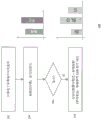
FIG. 1 is a flow diagram of an EDX method based on automated decision-making according to an embodiment of the present invention.
FIG. 2 is a flow diagram of a process flow for automated subsampling of identified defects according to an embodiment of the present invention.
FIG. 3 is a flow chart of a process flow for automated EDX review in array mode according to an embodiment of the present invention.
FIG. 4 shows an electron micrograph depicting a defect of interest (DOI) and corresponding reference points in neighboring cells, according to an embodiment of the invention.
FIG. 5 is a flow diagram of a process flow for automated EDX review in non-array mode according to an embodiment of the invention.
FIG. 6 shows an electron micrograph depicting defects of interest (DOI) and corresponding reference points on a reference die, according to an embodiment of the invention.
Fig. 7 is a flow diagram of an automated process for combining morphological defect results with elemental defect results to obtain final pareto (pareto), according to an embodiment of the invention.
Fig. 8 is a diagram in accordance with comparing an existing process for automated EDX review with an invented process for automated EDX review in accordance with an embodiment of the present invention.
FIG. 9 is a schematic diagram of a scanning electron microscope device with an energy dispersive x-ray (EDX) detection system according to an embodiment of the present invention.
Detailed Description
FIG. 1 is a flow diagram of an EDX method 100 based on automated decision-making according to an embodiment of the present invention. This method 100 may be performed after the defective locations are identified by automated inspection. For example, such automated inspection may be performed by the same or separate SEM equipment. The target substrate being inspected may be, for example, a silicon wafer having a plurality of dies formed thereon. Alternatively, the target substrate may be a reticle.
Referring to step 101, SEM automated review of the identified defects may be performed. SEM automated review may involve high resolution SEM imaging of defects identified in the results file from automated inspection.
Referring to step 102, after SEM automated review, morphology-based automated classification may be performed. As depicted in the example bar graph to the right of step 102, defects may be classified into defect types. The bar graph shows the relationship of defect frequency to defect type. Three types (#1, #2, and #3) are depicted, but the number of types can of course be any number. For example, the first defect type may be a hole, the second defect type may be a scratch, and the third defect type may be a particle. These are just a few exemplary defect types. Of course, other and different defect types may be utilized. For example, instead of having a particle defect type, there may be a large particle defect type and a small particle defect type depending on the size of the particle, or there may be a circular particle defect type and a non-circular particle defect type depending on the shape of the particle.
Referring to step 104, a selection of the type(s) of defects for automated EDX review is made. The selection of defect types for automated EDX review may be pre-programmed or pre-configured for automatic execution by executable program code executing the EDX method 100 based on automated decisions. As depicted in the example bar graph to the right of step 104, the selected type may be type # 3. For example, type # 3 may correspond to a defect type associated with the particle, which may also be referred to as a "fall on" defect. Such automated selection of defect types for automated EDX review according to step 104 may be referred to herein as automated (auto) subsampling. Further description of automated subsampling is provided below with respect to fig. 2.
After the automated sub-sampling of step 104, an automated EDX review 105 with accurate reference data may be performed on the selected type of defect. To obtain accurate reference data, automated EDX review 105 may involve repeating steps 106-116 for each defect of the selected type.
Referring to step 106, movement to the defect site may be performed. The movement to the defect site may be achieved by: translating the stage so that the defect site is within the field of view of the SEM. This operation may be performed based on the positional coordinates of the defect sites obtained from the stored results of the SEM automated review.
Referring to step 108, an EDX spectrum (defect spectrum) is obtained from the defect site. This operation may involve: translating the substrate so that the defect site is in the field of view of the SEM; and scanning the primary electron beam over the defect site while detecting an energy spectrum of the x-rays generated thereby. The defect spectra from each defect site may be stored in a manner so as to be associated with the location (coordinates) of the defect site.
Referring to step 110, movement from the defect site to a reference site correspondingly aligned with the defect site may be performed. As described further below with respect to fig. 3, if a defect site is indicated as being in the array of repeating cells, movement to the reference site may be achieved by deflecting the primary electron beam to a corresponding position in an adjacent cell. As described further below with respect to fig. 5, if the defect site is indicated as being in a non-array patterned structure (i.e., the patterned structure is not an array of repeating units), movement to the reference site may be achieved by translating the stage to a corresponding position on an adjacent die on a target substrate. An indication of whether the defect site is in an array-patterned structure or a non-array-patterned structure may be provided by data in the results file.
Referring to step 112, an EDX spectrum (reference spectrum) is obtained from the reference site. This operation may involve scanning the primary electron beam over a reference site while detecting the energy spectrum of the x-rays thus generated. The reference spectra may be stored in a manner so as to be associated with the corresponding defect sites.
Referring to step 114, a difference spectrum may be generated. In one implementation, normalization of the defect spectrum and the corresponding reference spectrum may be performed, and the normalized reference spectrum may be subtracted from the normalized defect spectrum to obtain a difference spectrum.
Referring to step 116, elemental information of the defect may be obtained from the difference spectrum. For example, if the selected defect type is a grain type, the elemental information may indicate an elemental composition of the grain. Advantageously, the elemental information obtained using the methods disclosed herein is more accurate than elemental information obtained from conventional automated EDX review procedures. This is because the methods disclosed herein locate the reference site more accurately than previous methods.
Exemplary bar graphs are provided to the right of steps 106 through 116. As seen in the example bar graph, the elemental information of the particle defect may indicate that the particle defect has an elemental composition that is primarily silicon (Si) or primarily carbon (C) or primarily iron (Fe).
Referring to step 118, the more accurate elemental information obtained using the presently disclosed method may be combined with the morphological information from step 102. An example bar graph with combined information is provided to the right of step 118. The bar graph shows the relationship of defect frequency to defect type. As shown in the example bar graph, four types of defect bins are depicted. The first two types (#1 and #2) correspond to the morphology-based types discussed above with respect to step 102 (holes and scratches, respectively). In this case, both the third type (#3) and the fourth type (#4) may be directed to particles depending on their elemental compositions. For example, the fourth type (#4) may correspond to particles whose composition is primarily (Fe), while the third type (#3) may correspond to particles of other compositions (i.e., not Fe). Note that this example is provided for illustrative purposes. Other defect types may be provided with different combinations of morphological information and elemental information.
FIG. 2 is a flow diagram of a process flow 200 for automated subsampling of identified defects according to an embodiment of the present invention. Automated sub-sampling advantageously reduces the number of defects to which EDX review applies, and thus reduces the time required to perform automated EDX review. This is because EDX review only applies to defects of a selected type (or several selected types), and not to all defects identified in the result file from automated inspection.
Referring to step 202, SEM automated review of the identified defects may be performed. SEM automated review may involve high resolution SEM imaging of defects identified in the results file from automated inspection.
Referring to step 204, the defects may be classified (i.e., "binned") into defect types. In this example, the defects may be classified into "fall-on" (particle) defect types and "other" (non-particle) defect types, as shown in the bar graph to the right of step 204.
Referring to step 206, a selection of only defects of the "fall on" defect type is made for EDX review. In other words, automated subsampling selects only fall-on defects for EDX review, while EDX review is not performed on other defects.
Referring to step 208, EDX review is performed on the selected defects in an automated manner. According to embodiments of the present invention, automated EDX review may be performed with accurate reference spectra using the automated EDX program 105 with accurate reference spectra described above with respect to fig. 1. For example, as shown in the bar graph to the right of step 208, the fall-on defects may be classified (binned) into a silicon (Si) particle type, a silicon oxide (Si, O) particle type, and a carbon (C) particle type.
FIG. 3 is a flow chart of a process flow for automated EDX review in array mode according to an embodiment of the present invention. The array pattern can be used for areas on a target substrate where an array of repeating cells is patterned. For example, the target substrate may include an array of memory cells, and the array pattern may be used for automated EDX review inside the array of memory cells.
Referring to step 302, automated inspection may be performed to detect defects in a target substrate. For example, automated inspection may be performed using SEM-based automated inspection equipment. The inspection tool may be integrated with or separate from the SEM-based automated review equipment.
Referring to step 304, data regarding defects detected by automated inspection may be stored in a result file. The information contains coordinate data about the location of the defect.
Referring to step 306, SEM automated review of detected defects in the array may be performed. SEM automated review may involve, among other steps, high resolution SEM imaging of defects identified in the results file from automated inspection.
Referring to step 308, the defects may be classified (i.e., "binned") into defect types. This classification can be made based on the morphology of the defects as can be observed from high resolution SEM imaging. For example, the defect types may include a hole type, a scratch type, and a particle ("fall on") type. These are just a few exemplary defect types. Of course, other and different defect types may be utilized.
Referring to step 310, this step may be performed for each defect in the result file. In this step, a defect in the results file may be selected as a defect of interest (DOI), and a determination may be made as to whether EDX review is to be applied to the DOI. This determination may be made in an automated manner based on the defect type of the DOI. If no EDX review is applied to the DOI, processing of the current DOI may end, and the method 300 may loop back and perform step 310 for the next defect, if any, selected to be the DOI. On the other hand, if an EDX review is to be applied to the DOI, the method 300 may proceed to perform steps 312-316.
With respect to step 312, EDX is applied to the DOI. This operation may involve: translating the stage to move the location of the DOI to be within the field of view; and EDX spectra were obtained from DOI.
With respect to step 314, EDX is applied to the corresponding location in the reference cell. This operation may involve deflecting the primary electron beam in one direction by a distance equal to the cell size in that direction. This deflection moves the primary electron beam so that it impinges on a location (reference point) in the adjacent cell (reference cell) corresponding to the location of the DOI in its cell. EDX spectra can then be obtained from the reference point.
With respect to step 316, a difference spectrum between the EDX spectrum of the DOI and the EDX spectrum of the reference point may be generated. The EDX spectra may be normalized before the difference spectra are generated. Thereafter, the difference spectrum may be used to obtain elemental information about the DOI, as described above with respect to step 116 in fig. 1.
FIG. 4 shows an electron micrograph depicting a defect of interest (DOI)402 and corresponding reference points 404 in neighboring cells, according to an embodiment of the invention. In this case, DOI 402 is within the repeating cell array. In this manner, automated EDX can be performed in an array mode, where the reference spectra are obtained by deflecting the electron beams by the width (or height) of the cells in the array.
FIG. 5 is a flow diagram of a process flow for automated EDX review in non-array mode according to an embodiment of the invention. A non-array ("random") pattern may be used for regions of the target substrate that are not patterned with an array of repeating cells. For example, an application specific integrated circuit may include a region with custom logic circuitry, and a non-array mode may be used for automated EDX review within this region.
Referring to step 502, automated inspection may be performed to detect defects in a target substrate. For example, automated inspection may be performed using SEM-based automated inspection equipment. The inspection tool may be integrated with or separate from the SEM-based automated review equipment.
Referring to step 504, data regarding defects detected by automated inspection may be stored in a result file. The information contains coordinate data about the location of the defect.
Referring to step 506, SEM automated review of the detected defects may be performed. In this case, the defect may be in a region that is not a repeating cell array (i.e., a non-array region), so that automated review can be performed in a "random" (non-array) mode. SEM automated review may involve, among other steps, high resolution SEM imaging of defects identified in the results file from automated inspection.
Referring to step 508, the defects may be classified (i.e., "binned") into defect types. This classification can be made based on the morphology of the defects as can be observed from high resolution SEM imaging. For example, the defect types may include a hole type, a scratch type, and a particle ("fall on") type. These are just a few exemplary defect types. Of course, other and different defect types may be utilized.
Referring to step 510, this step may be performed for each defect in the result file. In this step, a defect in the results file may be selected as a defect of interest (DOI), and a determination may be made as to whether EDX review is to be applied to the DOI. This determination may be made in an automated manner based on the defect type of the DOI. If no EDX review is applied to the DOI, processing of the current DOI may end, and the method 500 may loop back and perform step 510 for the next defect, if any, selected to be the DOI. On the other hand, if an EDX review is to be applied to the DOI, the method 500 may proceed to perform steps 512 through 520.
With respect to step 512, electron beam imaging may be performed in a field of view centered on the defect location coordinates of the DOI on the defective die in order to image an area surrounding the defect site. Preferably, the image of the region surrounding the defect site may be a high resolution image.
With respect to step 514, EDX is applied to the DOI to obtain an EDX spectrum (defect spectrum) of the DOI. The elemental information from this EDX spectrum contains not only elemental information from the DOI, but also elemental information from the material surrounding the DOI.
With respect to step 516, electron beam imaging may be performed in a field of view centered on the defect location coordinates on the reference die (rather than the defective die) in order to image an area surrounding the reference site. Preferably, the image of the area surrounding the reference site may be a high resolution image.
After step 514 and before step 516, the stage holding the target substrate is translated to move from the defective site on the defective die to a reference site on a reference die (which is preferably adjacent to the defective die). Further, the pattern of the image surrounding the reference site may be aligned to the pattern of the image surrounding the defect site, and the aligned images may be used to determine the position of the reference site with high accuracy.
With respect to step 518, EDX is applied to the reference site to obtain an EDX spectrum (reference spectrum) from the reference point. After normalization, this reference spectrum may be subtracted from the defect spectrum to obtain a difference spectrum, as indicated in step 520. Thereafter, the difference spectrum may be used to obtain elemental information about the DOI, as described above with respect to step 116 in fig. 1.
FIG. 6 shows an electron micrograph depicting defects of interest (DOI) and corresponding reference points on a reference die, according to an embodiment of the invention. In this case, the DOI is within the non-array portion of the die. As such, automated EDX may be performed in non-array mode, where a reference spectrum is obtained by first locating a reference point on a reference die, and stage translation is used to move between the DOI and the reference point.
FIG. 7 is a flow diagram of an automated process for combining morphological defect results with elemental defect results to obtain final pareto, according to an embodiment of the invention.
Referring to step 702, SEM automated review of detected defects may be performed. SEM automated review may involve, among other steps, high resolution SEM imaging of defects identified in the results file from automated inspection.
Referring to step 704, automated classification of defects may be performed based on morphology of the defects. Defects may be classified (i.e., "binned") into defect types, and each defect type may be represented by a category code. For example, the defect types may include a hole type as type 1, a scratch type as type 2, and a particle ("fall on") type as type 3. These are just a few exemplary defect types. Of course, other and different defect types may be utilized.
Referring to step 706, defects of a particular category code may be selected for automated EDX review while automated EDX review may be skipped for defects of other category codes. In other words, for each defect, a determination may be made as to whether the defect has a particular class code. If the category code is not a particular category code, then automated EDX review of the current defect is not performed, and the method 700 may loop back and perform step 706 for the next defect (if any). On the other hand, if the category code is a particular category code, method 700 may proceed to perform steps 708 and 710.
Referring to step 708, an automated EDX review is performed for defects of a particular class of code. To provide an accurate reference spectrum, automated EDX review may be performed with steps 312-316 described above with respect to fig. 3 if the defect being reviewed is within the repeat cell array, or with steps 512-520 if the defect being reviewed is not within this array region. As a result of step 708, a difference spectrum may be obtained for each defect of a particular class code.
Referring to step 710, the elemental composition of each defect of a particular class code may be obtained using the difference spectrum, and the defects of the particular class code may be binned based on the elemental composition of the defects of the particular class code. For example, if a particular category code corresponds to a particle or "fall on" defect, these defects may be separated into elemental composition bins based on their elemental composition. For example, elemental composition bins may include silicon (Si) bins, silicon oxide (Si, O) bins, and carbon (C) bins.
Referring to step 712, a defect pareto (final pareto) may be generated that is used in classifying defects and combines both morphological and elemental information. The defect pareto is a bar graph of defect frequency versus type. The defect pareto may be used to make decisions about what corrective actions need to be taken to reduce the defect rate. In one implementation, defects having a particular class code may be partitioned based on their elemental composition.
For example, consider that the morphological defect types from step 704 include a hole type as type 1, a scratch type as type 2, and a particle ("fall on") type as type 3. Consider further that the particular category code used to select defects for automated EDX review in step 706 is a category code of type 3 (particle or "fall on" defect). It is further contemplated that these fall-on defects may be classified based on the elemental composition of the particles. For example, an attachment defect of silicon oxide may be encoded as type 4, while attachment defects having other compositions (e.g., Si or C) may remain encoded as type 3. The resulting bar graph to the left of step 712 depicts the final pareto in this example.
Fig. 8 is a diagram comparing an existing process 800 for automated EDX review with an invented process 850 for automated EDX review, according to an embodiment of the invention. As depicted, the invented process 850 advantageously requires fewer steps and provides results more quickly than the existing process 800.
The existing process 800 comprises the following steps: requesting 802 review work by an operator; transferring 804 the wafer to be reviewed by SEM to a review tool (which may take approximately 15 minutes); performing 806 automated SEM review (which may take approximately 10 minutes); offline classification of defects into defect types (which may take approximately 30 minutes) is performed 808 by the operator; requesting 810EDX work by an operator for a set of defects (e.g., fall-on defects) classified under a selected type; transferring 812 the wafer to be reviewed by EDX to an EDX tool (which may take approximately 15 minutes); and then automated EDX may be performed 814 on the set of defects (which may take approximately 5 minutes).
As indicated, in the existing process 800, three steps ( steps 802, 808, and 810) require operator action. The existing process 850 may typically take about 75 minutes before the desired EDX data is obtained.
In contrast, the inventive process 850 includes the following steps: requesting 802 review work by an operator; transferring 804 the wafer to be reviewed by SEM to a review tool (which may take approximately 15 minutes); performing 806 automated SEM review (which may take approximately 5 minutes); and then a real-time EDX review may be performed 852 using the automated decision-based method 100 (see steps 102-118) described in a general manner above with respect to fig. 1.
As indicated, in the inventive process 850, only the first step (step 802), rather than the three steps in the existing process 800, requires operator action. Furthermore, the inventive process 850 may typically only take about 30 minutes before the desired EDX data is obtained (rather than about 75 minutes using the existing process 800).
FIG. 9 is a schematic diagram of a scanning electron microscope device 900 with an energy dispersive x-ray (EDX) detection system 920 according to an embodiment of the present invention. As shown in the cross-sectional view of fig. 9, an electron beam column may include a source 901, a Wien (Wien) filter, a scanning deflector 906, a focusing lens 907, an objective lens 908, and a translatable stage 919 holding a target substrate 910.
A source 901 generates an incident electron beam (primary electron beam) 902. The incident electron beam 902 may pass through a wien filter 904. Wien filter 904 is an electro-optical element configured to generate electric and magnetic fields that cross each other. A controllable electrostatic deflector 906 and a focusing electron lens 907 may be utilized. The deflector 906 can apply independently controllable electrostatic fields in the x-direction and in the y-direction. The deflector 906 may be controlled to scan the electron beam across the surface of the target substrate 910 or to deflect the electron beam for other purposes. For example, the target substrate 910 may be a patterned substrate, such as an integrated circuit being fabricated or a reticle for photolithography.
A focusing electron lens 907 is utilized to focus the incident electron beam 902 to a beam spot on the surface of a wafer or other substrate sample 910. According to one embodiment, the focusing lens 907 may be operated by generating electric and/or magnetic fields.
As a result of the scanning of the incident electron beam 902, secondary electrons and x-rays are emitted or scattered from a target substrate 910 (which may be, for example, a semiconductor wafer or reticle). The target substrate 910 may be held by a movable stage 911.
Secondary electrons may be extracted from the target substrate 910 by exposure to the electromagnetic field of the objective (final) lens 908. The electromagnetic field serves to confine the emitted electrons to a relatively small distance from the optical axis of the incident electron beam and to accelerate these electrons up into the column. In this way, a secondary electron beam 912 is formed from the secondary electrons.
The wien filter 904 deflects the secondary electron beam 912 from the optical axis of the incident electron beam 902 to a detection axis, which is the optical axis of a Secondary Electron (SE) detection system 914 for the apparatus. This serves to separate the scattered electron beam 912 from the incident electron beam 902. The SE detection system 914 detects the secondary electron beam 912 and generates data signals that can be used to form an image of the surface of the target substrate.
The instrument control and data processing (control/processing) system 950 may include one or more processors (i.e., microprocessors or microcontrollers) 952, data storage (including, for example, hard disk drive storage and memory chips) 954, a user interface 957, and a display system 958. Data storage 954 may store or hold computer-readable program code (instructions) 955 and data 956, and processor 952 may execute program code 955 and process data 956. User interface 957 may receive user input. The display system 958 may be configured to display image data and other information to a user.
The control/processing system 950 may be connected to and may be used to control various components of an electron beam column in order to implement the methods or procedures disclosed herein. For example, movement of the stage 911 and scanning by the deflector 906 may be controlled by computer readable program code 955 executed by the control/processing system 950.
Additionally, control/processing system 950 may also process electronic image data from SE detection system 914 and x-ray data from EDX detection system 920. In particular, computer readable program code 955 in the control/processing system 950 can be used to implement procedures related to automated EDX methods as described herein.
Conclusion
The drawings described above are not necessarily to scale and are intended to be illustrative and not limiting to particular implementations. The particular size, geometry, and lens current of the magnetic objective lens will vary and depend on each implementation.
For example, the techniques described above may be used in automated inspection and inspection analysis systems and applied to the inspection and review of wafers, X-ray masks, and similar substrates in a production environment. Other uses may also exist.
In the previous description, numerous specific details were set forth to provide a thorough understanding of embodiments of the invention. However, the above description of illustrated embodiments of the invention is not intended to be exhaustive or to limit the invention to the precise forms disclosed. One skilled in the relevant art will recognize that the invention can be practiced without one or more of the specific details, or with other methods, components, etc. In other instances, well-known structures or operations are not shown or described in detail to avoid obscuring aspects of the invention. While specific embodiments of, and examples for, the invention are described herein for illustrative purposes, various equivalent modifications are possible within the scope of the invention, as those skilled in the relevant art will recognize.
These modifications can be made to the invention in light of the above detailed description. The terms used in the following claims should not be construed to limit the invention to the specific embodiments disclosed in the specification and the claims. Rather, the scope of the invention is to be determined by the appended claims, which are to be construed in accordance with established doctrines of claim interpretation.
Claims (14)
1. A method for automated review of defects detected in defective dies on a target substrate, the method comprising:
obtaining a result file containing the location of the defect;
performing an automated review of the defect using a secondary electron microscope SEM to obtain an electron beam image of the defect;
performing an automated classification of the defect into a first number of types based on a morphology of the defect as determined from the electron beam image;
selecting a particular type of defect for automated energy dispersive x-ray EDX review; and
performing the automated EDX review on the defects of the particular type,
wherein performing the automated EDX review comprises, for each defect of the particular type:
move to the defect site;
obtaining an EDX spectrum from the defect site;
moving from the defect site to a reference site;
obtaining the EDX spectrum from the reference site;
generating a difference spectrum from the EDX spectrum from the defect site and the EDX spectrum from the reference site;
deriving elemental information from the difference spectrum for each defect of the particular type;
classifying each defect of the particular type into a second number of types based on the elemental information; and
generating a defective pareto based on the first number of types and the second number of types, wherein the first number of types includes one of the second number of types.
2. The method of claim 1, wherein the defect site is indicated as being in an array of repeating units, and wherein the moving from the defect site to the reference site is performed by: the primary electron beam is deflected by the cell dimension in a direction such that the reference site is at a position in the neighboring cell corresponding to the defect site.
3. The method of claim 1, wherein the defect sites are indicated as being in a non-array patterned structure, the method further comprising:
performing electron beam imaging to obtain a first image of an area surrounding the defect site on the defective die;
performing electron beam imaging to obtain a second image of an area surrounding the reference site on an adjacent die; and
after aligning the second image to the first image, determining a location of the reference site in the second image.
4. The method of claim 3, wherein the moving from the defect site to the reference site is performed by: translating a stage holding the target substrate so as to move a field of view of the SEM from the defect site on the defective die to the reference site on the adjacent die.
5. The method of claim 1, wherein the defect pareto combines morphology information and elemental information by dividing the particular type of defect into a plurality of types based on morphology of the defect depending on elemental information.
6. The method of claim 5, wherein the defect pareto comprises a bar graph of defect frequency versus type.
7. The method of claim 5, wherein the defect pareto distinguishes between holes, scratches, and particles, and further distinguishes between fall-on particles of a first composition and fall-on particles of a second composition.
8. An apparatus for automated review of defects detected on a target substrate, the apparatus comprising:
an electron beam column for generating and focusing a primary electron beam onto a surface of the target substrate;
a movable stage for holding the target substrate under the primary electron beam;
a deflector for deflecting the primary electron beam;
an electron detector for detecting secondary electrons emitted from the surface of the target substrate due to the collision of the primary electron beam;
an x-ray detector configured to detect x-rays emitted from the surface of the target substrate due to impingement of the primary electron beam; and
a control system comprising a non-transitory data storage device for storing computer-readable code and data and further comprising a processor for executing the computer-readable code, wherein the computer-readable code comprises instructions to:
obtaining a result file that includes locations of the defects detected in defective dies on the target substrate;
performing an automated secondary electron microscope, SEM, review of the defect to obtain an electron beam image of the defect;
performing an automated classification of the defect into a first number of types based on a morphology of the defect as determined from the electron beam image;
selecting a particular type of defect for automated energy dispersive x-ray EDX review; and
performing the automated EDX review on the defects of the particular type,
wherein the instructions to perform the automated EDX review further comprise instructions to:
move to the defect site;
obtaining an EDX spectrum from the defect site;
moving from the defect site to a reference site;
obtaining the EDX spectrum from the reference site; and
generating a difference spectrum from the EDX spectrum from the defect site and the EDX spectrum from the reference site;
deriving elemental information from the difference spectrum for each defect of the particular type;
classifying each defect of the particular type into a second number of types based on the elemental information; and
generating a defective pareto based on the first number of types and the second number of types, wherein the first number of types includes one of the second number of types.
9. The apparatus of claim 8, wherein the defect site is indicated as being in an array of repeating cells, and wherein instructions to move from the defect site to the reference site comprise instructions to deflect a primary electron beam by a cell size in one direction.
10. The apparatus of claim 8, wherein the defect site is indicated as being in a non-array patterned structure, and wherein the instructions to perform the automated EDX review further comprise instructions to:
obtaining a first image of an area surrounding the defect site on the defective die using electron beam imaging;
obtaining a second image of an area surrounding the reference site on an adjacent die using electron beam imaging; and
after aligning the second image to the first image, determining a location of the reference site in the second image.
11. The apparatus of claim 10, wherein instructions to move from the defect site to the reference site comprise instructions to translate the stage holding the target substrate so as to move a field of view of the SEM from the defect site on the defective die to the reference site on the adjacent die.
12. The apparatus of claim 8, wherein the defect pareto combines morphology information and elemental information by dividing the particular type of defect into a plurality of types based on morphology of the defect depending on elemental information.
13. The apparatus of claim 12, wherein the defect pareto comprises a bar graph of defect frequency versus type.
14. The apparatus of claim 12, wherein the defective pareto distinguishes between holes, scratches, and particles, and further distinguishes between fall-on particles of a first composition and fall-on particles of a second composition.
Applications Claiming Priority (13)
| Application Number | Priority Date | Filing Date | Title |
|---|---|---|---|
| US201462069048P | 2014-10-27 | 2014-10-27 | |
| US62/069,048 | 2014-10-27 | ||
| US201562159180P | 2015-05-08 | 2015-05-08 | |
| US62/159,180 | 2015-05-08 | ||
| US201562171698P | 2015-06-05 | 2015-06-05 | |
| US62/171,698 | 2015-06-05 | ||
| IN3080CH2015 | 2015-06-19 | ||
| IN3080/CHE/2015 | 2015-06-19 | ||
| US201562204325P | 2015-08-12 | 2015-08-12 | |
| US62/204,325 | 2015-08-12 | ||
| US14/919,563 US9696268B2 (en) | 2014-10-27 | 2015-10-21 | Automated decision-based energy-dispersive x-ray methodology and apparatus |
| US14/919,563 | 2015-10-21 | ||
| CN201580055501.2A CN106796188A (en) | 2014-10-27 | 2015-10-27 | Energy-dispersed X-ray method and device based on automatic decision-making |
Related Parent Applications (1)
| Application Number | Title | Priority Date | Filing Date |
|---|---|---|---|
| CN201580055501.2A Division CN106796188A (en) | 2014-10-27 | 2015-10-27 | Energy-dispersed X-ray method and device based on automatic decision-making |
Publications (1)
| Publication Number | Publication Date |
|---|---|
| CN111982953A true CN111982953A (en) | 2020-11-24 |
Family
ID=55791780
Family Applications (2)
| Application Number | Title | Priority Date | Filing Date |
|---|---|---|---|
| CN201580055501.2A Pending CN106796188A (en) | 2014-10-27 | 2015-10-27 | Energy-dispersed X-ray method and device based on automatic decision-making |
| CN202010883345.1A Pending CN111982953A (en) | 2014-10-27 | 2015-10-27 | Method and apparatus for automated review of defects detected on a target substrate |
Family Applications Before (1)
| Application Number | Title | Priority Date | Filing Date |
|---|---|---|---|
| CN201580055501.2A Pending CN106796188A (en) | 2014-10-27 | 2015-10-27 | Energy-dispersed X-ray method and device based on automatic decision-making |
Country Status (8)
| Country | Link |
|---|---|
| US (1) | US9696268B2 (en) |
| JP (1) | JP6814733B2 (en) |
| KR (1) | KR102219788B1 (en) |
| CN (2) | CN106796188A (en) |
| DE (1) | DE112015004853T5 (en) |
| SG (1) | SG11201702727SA (en) |
| TW (1) | TWI656340B (en) |
| WO (1) | WO2016069523A1 (en) |
Cited By (2)
| Publication number | Priority date | Publication date | Assignee | Title |
|---|---|---|---|---|
| CN114361057A (en) * | 2021-12-27 | 2022-04-15 | 广州粤芯半导体技术有限公司 | Defect detection method for semiconductor device and electronic equipment |
| WO2022134305A1 (en) * | 2020-12-21 | 2022-06-30 | 东方晶源微电子科技(北京)有限公司 | Wafer defect detection method and apparatus, device and storage medium |
Families Citing this family (10)
| Publication number | Priority date | Publication date | Assignee | Title |
|---|---|---|---|---|
| US9778215B2 (en) * | 2012-10-26 | 2017-10-03 | Fei Company | Automated mineral classification |
| US9696268B2 (en) * | 2014-10-27 | 2017-07-04 | Kla-Tencor Corporation | Automated decision-based energy-dispersive x-ray methodology and apparatus |
| KR102409943B1 (en) * | 2017-11-29 | 2022-06-16 | 삼성전자주식회사 | Method of detecting a defect and apparatus for performing the same |
| JP6679049B2 (en) | 2018-09-28 | 2020-04-15 | 株式会社リガク | Measuring device, program, and control method of measuring device |
| US10928336B1 (en) * | 2019-07-29 | 2021-02-23 | Applied Materials Israel Ltd. | X-ray based evaluation of a status of a structure of a substrate |
| DE102019126200A1 (en) * | 2019-09-27 | 2021-04-01 | Carl Zeiss Microscopy Gmbh | EDX process |
| US20240127417A1 (en) * | 2019-10-18 | 2024-04-18 | Hitachi High-Tech Corporation | Inspection System and Non-Transitory Computer-Readable Medium |
| EP3995808B1 (en) | 2020-11-09 | 2023-01-04 | Siltronic AG | Method for classifying unknown particles on a surface of a semiconductor wafer |
| DE102021117592B9 (en) | 2021-07-07 | 2023-08-03 | Carl Zeiss Microscopy Gmbh | Method for operating a particle beam microscope, particle beam microscope and computer program product |
| CN116130377B (en) * | 2023-04-17 | 2023-09-29 | 西安奕斯伟材料科技股份有限公司 | Epitaxial wafer defect detection method, device, system and manufacturing method thereof |
Citations (2)
| Publication number | Priority date | Publication date | Assignee | Title |
|---|---|---|---|---|
| US20030118149A1 (en) * | 2001-09-28 | 2003-06-26 | Hitachi, Ltd. | Defect inspection apparatus and defect inspection method |
| US20050033528A1 (en) * | 2003-04-29 | 2005-02-10 | Kla-Tencor Technologies, Corporation | Single tool defect classification solution |
Family Cites Families (53)
| Publication number | Priority date | Publication date | Assignee | Title |
|---|---|---|---|---|
| JP2787924B2 (en) * | 1989-06-29 | 1998-08-20 | 株式会社島津製作所 | Electron beam micro analyzer |
| JP2922940B2 (en) | 1989-11-22 | 1999-07-26 | 株式会社日立製作所 | Energy dispersive X-ray analyzer |
| US5263075A (en) | 1992-01-13 | 1993-11-16 | Ion Track Instruments, Inc. | High angular resolution x-ray collimator |
| US5649169A (en) * | 1995-06-20 | 1997-07-15 | Advanced Micro Devices, Inc. | Method and system for declustering semiconductor defect data |
| US5656812A (en) * | 1995-07-21 | 1997-08-12 | Jeol Ltd. | Electron probe microanalyzer and X-ray analysis using same |
| US6259960B1 (en) * | 1996-11-01 | 2001-07-10 | Joel Ltd. | Part-inspecting system |
| JP3500264B2 (en) | 1997-01-29 | 2004-02-23 | 株式会社日立製作所 | Sample analyzer |
| JP3101257B2 (en) * | 1998-01-30 | 2000-10-23 | 理学電機工業株式会社 | Method for inspecting sample surface and X-ray analyzer using the same |
| US6442233B1 (en) | 1998-06-18 | 2002-08-27 | American Science And Engineering, Inc. | Coherent x-ray scatter inspection system with sidescatter and energy-resolved detection |
| EP1121584A4 (en) | 1998-09-17 | 2002-10-16 | Noran Instr Inc | Application of x-ray optics to energy dispersive spectroscopy |
| US6407386B1 (en) | 1999-02-23 | 2002-06-18 | Applied Materials, Inc. | System and method for automatic analysis of defect material on semiconductors |
| JP2001153826A (en) * | 1999-11-26 | 2001-06-08 | Matsushita Electronics Industry Corp | Device and method for x-ray photoelectron spectroscopy |
| JP4312910B2 (en) * | 1999-12-02 | 2009-08-12 | 株式会社日立製作所 | Review SEM |
| US6528818B1 (en) | 1999-12-14 | 2003-03-04 | Kla-Tencor | Test structures and methods for inspection of semiconductor integrated circuits |
| US6787773B1 (en) | 2000-06-07 | 2004-09-07 | Kla-Tencor Corporation | Film thickness measurement using electron-beam induced x-ray microanalysis |
| JP3804757B2 (en) | 2000-09-05 | 2006-08-02 | 株式会社日立製作所 | Micropart analyzer and analysis method |
| US6744266B2 (en) | 2000-10-02 | 2004-06-01 | Applied Materials, Inc. | Defect knowledge library |
| JP4178741B2 (en) | 2000-11-02 | 2008-11-12 | 株式会社日立製作所 | Charged particle beam apparatus and sample preparation apparatus |
| US6990086B1 (en) * | 2001-01-26 | 2006-01-24 | Cisco Technology, Inc. | Method and system for label edge routing in a wireless network |
| US6423557B1 (en) | 2001-03-15 | 2002-07-23 | Advanced Micro Devices, Inc. | ADC based in-situ destructive analysis selection and methodology therefor |
| US6753261B1 (en) | 2002-01-17 | 2004-06-22 | Advanced Micro Devices, Inc. | In-situ chemical composition monitor on wafer during plasma etching for defect control |
| CN100458712C (en) * | 2002-11-12 | 2009-02-04 | Fei公司 | Defect characterization system and method and defect analysis system |
| JP3993817B2 (en) * | 2002-12-11 | 2007-10-17 | 株式会社日立製作所 | Defect composition analysis method and apparatus |
| JP3888980B2 (en) | 2003-03-18 | 2007-03-07 | 株式会社日立ハイテクノロジーズ | Material identification system |
| US7132652B1 (en) | 2003-03-25 | 2006-11-07 | Kla-Tencor Technologies Corporation | Automatic classification of defects using pattern recognition applied to X-ray spectra |
| US7092485B2 (en) | 2003-05-27 | 2006-08-15 | Control Screening, Llc | X-ray inspection system for detecting explosives and other contraband |
| JP2005114384A (en) * | 2003-10-03 | 2005-04-28 | Hitachi High-Technologies Corp | Defect elemental analysis method and apparatus |
| JP4931799B2 (en) | 2004-03-22 | 2012-05-16 | ケーエルエー−テンカー コーポレイション | Method and system for measuring substrate characteristics or preparing a substrate for analysis |
| KR20070010472A (en) * | 2005-07-19 | 2007-01-24 | 삼성전자주식회사 | Hybrid polarizer, manufacturing method thereof and display device having same |
| WO2007015472A1 (en) | 2005-08-04 | 2007-02-08 | Sii Nanotechnology Inc. | X-ray analyzer and analyzing method |
| JP4533306B2 (en) * | 2005-12-06 | 2010-09-01 | 株式会社日立ハイテクノロジーズ | Semiconductor wafer inspection method and defect review apparatus |
| JP4644613B2 (en) * | 2006-02-27 | 2011-03-02 | 株式会社日立ハイテクノロジーズ | Defect observation method and apparatus |
| JP4825021B2 (en) | 2006-02-28 | 2011-11-30 | 株式会社日立ハイテクノロジーズ | Report format setting method, report format setting device, and defect review system |
| JP4307470B2 (en) * | 2006-08-08 | 2009-08-05 | 株式会社日立ハイテクノロジーズ | Charged particle beam apparatus, sample processing method, and semiconductor inspection apparatus |
| US7397556B2 (en) * | 2006-10-31 | 2008-07-08 | International Business Machines Corporation | Method, apparatus, and computer program product for optimizing inspection recipes using programmed defects |
| US7904845B2 (en) | 2006-12-06 | 2011-03-08 | Kla-Tencor Corp. | Determining locations on a wafer to be reviewed during defect review |
| JP5164598B2 (en) * | 2008-02-18 | 2013-03-21 | 株式会社日立ハイテクノロジーズ | Review method and review device |
| JP2010078478A (en) * | 2008-09-26 | 2010-04-08 | Toshiba Corp | Apparatus and method for inspecting defect |
| EP2284524B1 (en) | 2009-08-10 | 2014-01-15 | FEI Company | Microcalorimetry for X-ray spectroscopy |
| US9518808B2 (en) * | 2010-02-16 | 2016-12-13 | Research Foundation Of State University Of New York | Ammunition and weapon type identification based on spectroscopic gunshot residue analysis |
| WO2011151116A1 (en) | 2010-06-03 | 2011-12-08 | Carl Zeiss Sms Gmbh | A method for determining the performance of a photolithographic mask |
| JP2012242146A (en) * | 2011-05-17 | 2012-12-10 | Hitachi High-Technologies Corp | Scanning electron microscope and sample preparation method |
| US8421007B2 (en) | 2011-05-18 | 2013-04-16 | Tohoku University | X-ray detection system |
| EP2605005A1 (en) | 2011-12-14 | 2013-06-19 | FEI Company | Clustering of multi-modal data |
| JP2013114854A (en) | 2011-11-28 | 2013-06-10 | Hitachi High-Technologies Corp | Sample observation device and marking method |
| JP6355318B2 (en) | 2012-11-15 | 2018-07-11 | 株式会社日立ハイテクサイエンス | Cross-section processing observation method and apparatus |
| TW201430336A (en) * | 2013-01-23 | 2014-08-01 | Huang Tian Xing | Defect detection method, device and system |
| JP5948262B2 (en) * | 2013-01-30 | 2016-07-06 | 株式会社日立ハイテクノロジーズ | Defect observation method and defect observation apparatus |
| KR102026936B1 (en) * | 2013-03-26 | 2019-10-01 | 삼성디스플레이 주식회사 | Inspection system using scanning electron microscope |
| JP6328456B2 (en) | 2014-03-20 | 2018-05-23 | 株式会社日立ハイテクサイエンス | Energy dispersive X-ray analyzer and energy dispersive X-ray analysis method |
| JP2015216285A (en) * | 2014-05-13 | 2015-12-03 | 株式会社日立ハイテクノロジーズ | Defect analysis method |
| US9218940B1 (en) * | 2014-05-30 | 2015-12-22 | Fei Company | Method and apparatus for slice and view sample imaging |
| US9696268B2 (en) * | 2014-10-27 | 2017-07-04 | Kla-Tencor Corporation | Automated decision-based energy-dispersive x-ray methodology and apparatus |
-
2015
- 2015-10-21 US US14/919,563 patent/US9696268B2/en active Active
- 2015-10-22 TW TW104134805A patent/TWI656340B/en active
- 2015-10-27 JP JP2017521139A patent/JP6814733B2/en active Active
- 2015-10-27 SG SG11201702727SA patent/SG11201702727SA/en unknown
- 2015-10-27 CN CN201580055501.2A patent/CN106796188A/en active Pending
- 2015-10-27 WO PCT/US2015/057455 patent/WO2016069523A1/en not_active Ceased
- 2015-10-27 KR KR1020177014282A patent/KR102219788B1/en active Active
- 2015-10-27 DE DE112015004853.7T patent/DE112015004853T5/en not_active Ceased
- 2015-10-27 CN CN202010883345.1A patent/CN111982953A/en active Pending
Patent Citations (2)
| Publication number | Priority date | Publication date | Assignee | Title |
|---|---|---|---|---|
| US20030118149A1 (en) * | 2001-09-28 | 2003-06-26 | Hitachi, Ltd. | Defect inspection apparatus and defect inspection method |
| US20050033528A1 (en) * | 2003-04-29 | 2005-02-10 | Kla-Tencor Technologies, Corporation | Single tool defect classification solution |
Cited By (2)
| Publication number | Priority date | Publication date | Assignee | Title |
|---|---|---|---|---|
| WO2022134305A1 (en) * | 2020-12-21 | 2022-06-30 | 东方晶源微电子科技(北京)有限公司 | Wafer defect detection method and apparatus, device and storage medium |
| CN114361057A (en) * | 2021-12-27 | 2022-04-15 | 广州粤芯半导体技术有限公司 | Defect detection method for semiconductor device and electronic equipment |
Also Published As
| Publication number | Publication date |
|---|---|
| WO2016069523A1 (en) | 2016-05-06 |
| JP6814733B2 (en) | 2021-01-20 |
| KR20170077184A (en) | 2017-07-05 |
| TW201627659A (en) | 2016-08-01 |
| CN106796188A (en) | 2017-05-31 |
| US20160116425A1 (en) | 2016-04-28 |
| TWI656340B (en) | 2019-04-11 |
| JP2017532564A (en) | 2017-11-02 |
| DE112015004853T5 (en) | 2017-07-13 |
| KR102219788B1 (en) | 2021-02-23 |
| US9696268B2 (en) | 2017-07-04 |
| SG11201702727SA (en) | 2017-05-30 |
Similar Documents
| Publication | Publication Date | Title |
|---|---|---|
| US9696268B2 (en) | Automated decision-based energy-dispersive x-ray methodology and apparatus | |
| JP5202071B2 (en) | Charged particle microscope apparatus and image processing method using the same | |
| US9502211B1 (en) | Adaptive scanning for particle size using directed beam signal analysis | |
| US9046344B2 (en) | Multiple image metrology | |
| KR20170026298A (en) | CAD-assisted TEM prep recipe creation | |
| JP2012242146A (en) | Scanning electron microscope and sample preparation method | |
| US10732512B2 (en) | Image processor, method for generating pattern using self-organizing lithographic techniques and computer program | |
| US20070187599A1 (en) | Charged particle beam apparatus, charged particle beam focusing method, microstructure measuring method, microstructure inspecting method, semiconductor device manufacturing method, and program | |
| US20130134308A1 (en) | Sample observation apparatus and method of marking | |
| CN116868300A (en) | High-resolution X-ray spectrometer surface material analysis | |
| KR20240069803A (en) | High-resolution, low-energy electron microscopy and mask inspection methods to provide topographic information | |
| CN111579890A (en) | Focused ion beam contaminant identification | |
| US11626267B2 (en) | Back-scatter electrons (BSE) imaging with a SEM in tilted mode using cap bias voltage | |
| US8309922B2 (en) | Semiconductor inspection method and device that consider the effects of electron beams | |
| US8110799B2 (en) | Confocal secondary electron imaging | |
| US6881956B1 (en) | Method and apparatus for scanning semiconductor wafers using a scanning electron microscope | |
| US9269533B2 (en) | Analysis apparatus and analysis method | |
| KR102001715B1 (en) | Methods and apparatus for measurement of relative critical dimensions | |
| EP3091558A1 (en) | Adaptive scanning for particle size using directed beam signal analysis | |
| WO2025104896A1 (en) | Defect inspection apparatus | |
| TW202541182A (en) | Systems and methods of sem inspection using selective scan approach | |
| JP2007220317A (en) | Electron beam inspection method and apparatus | |
| EP3098833A1 (en) | Adaptive scanning for particle size using directed beam signal analysis | |
| WO2015064399A1 (en) | Charged-particle-beam device and program recording medium |
Legal Events
| Date | Code | Title | Description |
|---|---|---|---|
| PB01 | Publication | ||
| PB01 | Publication | ||
| SE01 | Entry into force of request for substantive examination | ||
| SE01 | Entry into force of request for substantive examination |