CN111988499A - Imaging layer, imaging device, electronic equipment, zone plate structure and photosensitive pixel - Google Patents
Imaging layer, imaging device, electronic equipment, zone plate structure and photosensitive pixel Download PDFInfo
- Publication number
- CN111988499A CN111988499A CN201911243858.XA CN201911243858A CN111988499A CN 111988499 A CN111988499 A CN 111988499A CN 201911243858 A CN201911243858 A CN 201911243858A CN 111988499 A CN111988499 A CN 111988499A
- Authority
- CN
- China
- Prior art keywords
- light
- imaging
- zone plate
- plate structure
- layer
- Prior art date
- Legal status (The legal status is an assumption and is not a legal conclusion. Google has not performed a legal analysis and makes no representation as to the accuracy of the status listed.)
- Granted
Links
Images




Classifications
-
- H—ELECTRICITY
- H04—ELECTRIC COMMUNICATION TECHNIQUE
- H04N—PICTORIAL COMMUNICATION, e.g. TELEVISION
- H04N23/00—Cameras or camera modules comprising electronic image sensors; Control thereof
- H04N23/50—Constructional details
- H04N23/54—Mounting of pick-up tubes, electronic image sensors, deviation or focusing coils
-
- H—ELECTRICITY
- H04—ELECTRIC COMMUNICATION TECHNIQUE
- H04N—PICTORIAL COMMUNICATION, e.g. TELEVISION
- H04N23/00—Cameras or camera modules comprising electronic image sensors; Control thereof
- H04N23/95—Computational photography systems, e.g. light-field imaging systems
- H04N23/955—Computational photography systems, e.g. light-field imaging systems for lensless imaging
-
- G—PHYSICS
- G02—OPTICS
- G02B—OPTICAL ELEMENTS, SYSTEMS OR APPARATUS
- G02B27/00—Optical systems or apparatus not provided for by any of the groups G02B1/00 - G02B26/00, G02B30/00
- G02B27/42—Diffraction optics, i.e. systems including a diffractive element being designed for providing a diffractive effect
- G02B27/44—Grating systems; Zone plate systems
-
- H—ELECTRICITY
- H04—ELECTRIC COMMUNICATION TECHNIQUE
- H04N—PICTORIAL COMMUNICATION, e.g. TELEVISION
- H04N23/00—Cameras or camera modules comprising electronic image sensors; Control thereof
- H04N23/45—Cameras or camera modules comprising electronic image sensors; Control thereof for generating image signals from two or more image sensors being of different type or operating in different modes, e.g. with a CMOS sensor for moving images in combination with a charge-coupled device [CCD] for still images
-
- H—ELECTRICITY
- H04—ELECTRIC COMMUNICATION TECHNIQUE
- H04N—PICTORIAL COMMUNICATION, e.g. TELEVISION
- H04N23/00—Cameras or camera modules comprising electronic image sensors; Control thereof
- H04N23/50—Constructional details
-
- H—ELECTRICITY
- H04—ELECTRIC COMMUNICATION TECHNIQUE
- H04N—PICTORIAL COMMUNICATION, e.g. TELEVISION
- H04N23/00—Cameras or camera modules comprising electronic image sensors; Control thereof
- H04N23/50—Constructional details
- H04N23/55—Optical parts specially adapted for electronic image sensors; Mounting thereof
-
- H—ELECTRICITY
- H04—ELECTRIC COMMUNICATION TECHNIQUE
- H04N—PICTORIAL COMMUNICATION, e.g. TELEVISION
- H04N23/00—Cameras or camera modules comprising electronic image sensors; Control thereof
- H04N23/57—Mechanical or electrical details of cameras or camera modules specially adapted for being embedded in other devices
-
- H—ELECTRICITY
- H04—ELECTRIC COMMUNICATION TECHNIQUE
- H04N—PICTORIAL COMMUNICATION, e.g. TELEVISION
- H04N23/00—Cameras or camera modules comprising electronic image sensors; Control thereof
- H04N23/95—Computational photography systems, e.g. light-field imaging systems
- H04N23/958—Computational photography systems, e.g. light-field imaging systems for extended depth of field imaging
Landscapes
- Engineering & Computer Science (AREA)
- Multimedia (AREA)
- Signal Processing (AREA)
- Computing Systems (AREA)
- Theoretical Computer Science (AREA)
- Physics & Mathematics (AREA)
- Human Computer Interaction (AREA)
- General Physics & Mathematics (AREA)
- Optics & Photonics (AREA)
- Image Input (AREA)
Abstract
本申请公开一种成像层、成像装置、电子设备、波带片结构及感光像元,包括成像层和位于所述成像层下侧的图像传感器,所述成像层上设有若干个成像孔,每个所述成像孔内设有波带片结构,所述波带片结构包括遮光带和透光带,所述波带片结构使经目标物反射的光线汇聚于所述图像传感器上成像。在成像层上设置波带片结构,波带片结构是根据光干涉的原理计算设计得到,使得经过透光带的单色光相干增强汇聚于图像传感器上,进而使得汇聚在图像传感器上的光均为相干增强光线,极大的放大了光强。同时,由于增加了透光面积,由光的波动性产生的干涉/衍射的次峰的相对高度和其与主峰之间的距离也会降低。从而进一步提高了光学分辨率。
The present application discloses an imaging layer, an imaging device, an electronic device, a zone plate structure and a photosensitive pixel, comprising an imaging layer and an image sensor located on the lower side of the imaging layer, and a plurality of imaging holes are arranged on the imaging layer, Each of the imaging holes is provided with a zone plate structure, the zone plate structure includes a light-shielding zone and a light-transmitting zone, and the zone plate structure makes the light reflected by the object converge on the image sensor for imaging. A zone plate structure is arranged on the imaging layer. The zone plate structure is calculated and designed according to the principle of light interference, so that the coherence enhancement of the monochromatic light passing through the light transmission band is concentrated on the image sensor, thereby making the light converging on the image sensor. All are coherently enhanced light, which greatly amplifies the light intensity. At the same time, the relative height of the secondary peak of interference/diffraction caused by the wave nature of light and the distance between it and the main peak are also reduced due to the increased light transmission area. Thereby, the optical resolution is further improved.
Description
本申请要求于2019年5月22日提交中国国知局、申请号为201910430939.4的中国专利申请的优先权,其全部内容通过引用结合在本申请中。This application claims the priority of the Chinese patent application with application number 201910430939.4 filed on May 22, 2019 with the State Intellectual Property Office of China, the entire contents of which are incorporated herein by reference.
技术领域technical field
本申请涉及图像采集技术领域,具体涉及一种成像装置。此外,本申请还涉及一种成像层、电子设备、波带片结构及感光像元。The present application relates to the technical field of image acquisition, and in particular, to an imaging device. In addition, the present application also relates to an imaging layer, an electronic device, a zone plate structure and a photosensitive pixel.
背景技术Background technique
现有的移动终端,如手机等,希望做到全面屏设计,并且将指纹识别和前置摄像头集成于显示屏下同时不影响显示。现有技术中已经有将指纹识别集成于显示屏下的技术,例如在先专利CN201710086890.6中提出了一种矩阵式小孔成像系统(Matrix PinholeImaging System,MAPIS),用于近距离采集物体表面图像,如指纹图像、人脸图像等。MAPIS可以被应用在手机、平板电脑、智能手环等多种电子设备中。Existing mobile terminals, such as mobile phones, hope to achieve a full-screen design, and integrate fingerprint recognition and front-facing cameras under the display without affecting the display. There are technologies that integrate fingerprint recognition under the display screen in the prior art. For example, the prior patent CN201710086890.6 proposed a Matrix Pinhole Imaging System (MAPIS), which is used to collect object surfaces at close range. Images, such as fingerprint images, face images, etc. MAPIS can be applied to various electronic devices such as mobile phones, tablet computers, smart bracelets, etc.
MAPIS一般包括小孔板和图像传感器。在小孔板上开设有多个成像孔。图像传感器设置在小孔板的一侧,并且与成像孔的位置对应。这样,根据小孔成像原理,小孔板另一侧的目标物上的光线,就可以穿过成像孔,在图像传感器上形成目标物的倒立的像。穿过每一个成像孔的光线都可以在图像传感器上形成一个相应的像,将这多个像进行拼接,就可以得到一个相对完整的关于目标物的图像。MAPIS generally includes a small aperture plate and an image sensor. A plurality of imaging holes are opened on the small orifice plate. The image sensor is arranged on one side of the small orifice plate and corresponds to the position of the imaging hole. In this way, according to the principle of pinhole imaging, the light on the object on the other side of the pinhole plate can pass through the imaging hole to form an inverted image of the object on the image sensor. The light passing through each imaging hole can form a corresponding image on the image sensor, and by splicing these multiple images, a relatively complete image of the target can be obtained.
上述的MAPIS可以应用在具有显示屏的电子设备中,以用于采集指纹图像、人脸图像等。电子设备的显示屏包括阵列排布的发光像素,以及用于控制发光像素的电路。电路通常是不透明的,但是电路之间具有间隙,使显示屏上方的光线可以通过这些间隙,到达显示屏的下方。在显示屏的下方设置小孔板,通过小孔板上的成像孔的位置、大小和形状,来规范光线可以通过的区域。理想的小孔板上的成像孔孔径约为10-15μm。此时,通过成像孔的光线强度合适,衍射很小,故而在图像传感器上所形成的像的清晰度较高,分辨率较好,能够满足应用在具有显示屏的电子设备中的需求。The above-mentioned MAPIS can be applied to an electronic device with a display screen to collect fingerprint images, face images, and the like. A display screen of an electronic device includes light-emitting pixels arranged in an array, and a circuit for controlling the light-emitting pixels. The circuits are usually opaque, but there are gaps between the circuits that allow light above the display to pass through these gaps to the underside of the display. A small orifice plate is arranged below the display screen, and the area through which light can pass is regulated by the position, size and shape of the imaging holes on the small orifice plate. The diameter of the imaging wells on an ideal small well plate is about 10-15 μm. At this time, the intensity of the light passing through the imaging hole is suitable and the diffraction is small, so the image formed on the image sensor has high definition and good resolution, which can meet the needs of application in electronic equipment with a display screen.
但是,随着显示屏的分辨率越来越高,发光像素的排布越来越紧密,相应的电路也越来越多,这导致电路之间的间隙大幅减小(例如减小到约5μm),难以达到理想的成像孔孔径的要求。在成像孔孔径受到间隙的限制而大幅减小的情况下,通过成像孔的光线强度减小,衍射严重,进而导致这些光线难以被图像传感器接收,容易淹没在图像传感器的热噪声之中。However, as the resolution of the display screen becomes higher and higher, the arrangement of light-emitting pixels becomes more and more dense, and the corresponding circuits are also more and more, which leads to a significant reduction of the gap between the circuits (for example, to about 5 μm). ), it is difficult to achieve the ideal imaging aperture requirements. When the aperture of the imaging hole is greatly reduced due to the limitation of the gap, the intensity of the light passing through the imaging hole is reduced, and the diffraction is serious, which makes it difficult for the light to be received by the image sensor and is easily submerged in the thermal noise of the image sensor.
另一方面,现有技术中还不存在将前置摄像头集成于显示屏下并不影响显示的方案。最接近的方案有升降摄像头,水滴框,显示屏上开孔等。但是后两者都对显示有影响。On the other hand, there is no solution in the prior art that integrates the front camera under the display screen without affecting the display. The closest solution is a lift camera, a water drop frame, a hole in the display, etc. But both of the latter have an effect on the display.
在专利201811271636.4(申请号,尚未公开,有同日申请的实用新型)中,提出了一种屏下摄像头的方案。但是该方案也需要开一个相对较大的中心孔,并且需要搭配透镜使用。而由于透镜需要安置在显示屏下方,透镜的厚度会阻碍组装。In the patent 201811271636.4 (application number, not yet published, there is a utility model applied for on the same day), a solution for an under-screen camera is proposed. However, this solution also requires a relatively large central hole and needs to be used with a lens. And because the lens needs to be placed under the display, the thickness of the lens can hinder assembly.
发明内容SUMMARY OF THE INVENTION
本申请通过充分利用光的干涉增强特性,提供解决上述技术问题的成像层、应用该成像层的成像装置及电子设备。The present application provides an imaging layer that solves the above-mentioned technical problems, an imaging device and an electronic device using the imaging layer by making full use of the interference enhancement properties of light.
第一方面,本申请提供一种成像装置,包括成像层和位于所述成像层下侧的图像传感器,所述成像层上设有若干个成像孔,每个所述成像孔内设有波带片结构,所述波带片结构包括遮光带和透光带,所述波带片结构使经目标物反射的光线汇聚于所述图像传感器上成像。In a first aspect, the present application provides an imaging device, comprising an imaging layer and an image sensor located on a lower side of the imaging layer, the imaging layer is provided with a plurality of imaging holes, and each imaging hole is provided with a wave band The zone plate structure includes a light-shielding zone and a light-transmitting zone, and the zone plate structure makes the light reflected by the object converge on the image sensor for imaging.
结合第一方面,在第一方面第一种可能的实现方式中,当所述成像孔内波带片结构的透光带的面积总和大于遮光带的面积总和时,将所述遮光带去除。第二方面,本申请提供一种电子设备,包括所述的成像装置和显示屏,所述显示屏包括电路层;With reference to the first aspect, in a first possible implementation manner of the first aspect, when the total area of the light-transmitting bands of the zone plate structure in the imaging hole is greater than the total area of the light-shielding bands, the light-shielding bands are removed. In a second aspect, the present application provides an electronic device, including the imaging device and a display screen, the display screen including a circuit layer;
当所述电路层包括若干第一透光部分时,所述成像层上设有若干成像孔,所述成像孔内设有波带片结构,所述成像孔与所述第一透光部分对应;所述第一透光部分的面积足够设置至少一个波带片结构。When the circuit layer includes a plurality of first light-transmitting parts, the imaging layer is provided with a number of imaging holes, the imaging holes are provided with a zone plate structure, and the imaging holes correspond to the first light-transmitting parts ; The area of the first light-transmitting portion is sufficient to set at least one zone plate structure.
第三方面,本申请提供一种电子设备,包括显示屏、成像层和图像传感器;In a third aspect, the present application provides an electronic device, including a display screen, an imaging layer and an image sensor;
所述显示屏包括电路层,所述电路层包括若干第二透光部分;The display screen includes a circuit layer, and the circuit layer includes a plurality of second light-transmitting parts;
所述成像层位于所述电路层下方或上方;the imaging layer is below or above the circuit layer;
所述成像层包括若干成像孔,所述成像孔内设有波带片结构,所述成像层与所述电路层对齐,使所述成像层的透光带与所述电路层的第二透光部分重合,其中,一个所述波带片结构与多个所述第二透光部分对应;The imaging layer includes a plurality of imaging holes, the imaging holes are provided with a zone plate structure, and the imaging layer is aligned with the circuit layer, so that the light-transmitting band of the imaging layer is connected to the second transparent belt of the circuit layer. The light parts are overlapped, wherein one of the zone plate structures corresponds to a plurality of the second light-transmitting parts;
其中,所述波带片结构包括遮光带和透光带;当目标物接触所述显示屏时,经过目标物反射后,射入的光线穿过所述透光部分和透光带汇聚在所述图像传感上成像。Wherein, the wave zone plate structure includes a light-shielding belt and a light-transmitting belt; when the target object touches the display screen, after being reflected by the target object, the incident light passes through the light-transmitting part and the light-transmitting belt and converges on the display screen. imaged on the image sensor.
结合第三方面,在第一方面第一种可能的实现方式中,当所述成像层上开设有至少两个成像孔时,相邻的成像孔的像方视场不重合。With reference to the third aspect, in a first possible implementation manner of the first aspect, when the imaging layer is provided with at least two imaging holes, the image-side fields of view of adjacent imaging holes do not overlap.
结合第三方面及上述可能的实现方式,在第一方面第二种可能的实现方式中,当所述成像层上开设有至少两个成像孔时,相邻的成像孔的物方视场重合。In combination with the third aspect and the above possible implementation manners, in a second possible implementation manner of the first aspect, when at least two imaging holes are opened on the imaging layer, the object-side fields of view of adjacent imaging holes overlap. .
结合第三方面及上述可能的实现方式,在第一方面第三种可能的实现方式中,所述成像孔的数量为3个。In combination with the third aspect and the above possible implementation manners, in a third possible implementation manner of the first aspect, the number of the imaging holes is three.
结合第三方面及上述可能的实现方式,在第一方面第四种可能的实现方式中,所述电路层上还包括阵列排布的发光像素,减少单位面积内的发光像素数量,在缺失的发光像素对应的成像层上设有若干个成像孔,每个所述成像孔内设有波带片结构。In combination with the third aspect and the above possible implementation manners, in a fourth possible implementation manner of the first aspect, the circuit layer further includes light-emitting pixels arranged in an array, so as to reduce the number of light-emitting pixels per unit area. The imaging layer corresponding to the light-emitting pixel is provided with a plurality of imaging holes, and each of the imaging holes is provided with a zone plate structure.
结合第三方面及上述可能的实现方式,在第一方面第五种可能的实现方式中,相邻两个所述缺失的发光像素之间间隔有至少一个发光像素。With reference to the third aspect and the above possible implementation manners, in a fifth possible implementation manner of the first aspect, at least one light-emitting pixel is spaced between two adjacent missing light-emitting pixels.
结合第三方面及上述可能的实现方式,在第一方面第六种可能的实现方式中,所述图像传感器与所述成像层之间的距离设置满足使物面上一点发出的光线汇聚于图像传感器上的一点。In combination with the third aspect and the above possible implementation manners, in a sixth possible implementation manner of the first aspect, the distance between the image sensor and the imaging layer is set such that light emitted from a point on the object surface converges on the image. point on the sensor.
结合第三方面及上述可能的实现方式,在第三方面第七种可能的实现方式中,所述成像孔和所述波带片结构的透光带还用于电路线走线的通孔。In combination with the third aspect and the above possible implementation manners, in a seventh possible implementation manner of the third aspect, the imaging hole and the light-transmitting zone of the zone plate structure are also used for through holes for circuit wiring.
结合第三方面及上述可能的实现方式,在第三方面第八种可能的实现方式中,所述成像层与所述电路层对齐,使所述成像层的透光带与所述电路层的第二透光部分的重合面积最大或重合面积满足预设面积阈值范围。In combination with the third aspect and the above possible implementation manners, in an eighth possible implementation manner of the third aspect, the imaging layer is aligned with the circuit layer, so that the light-transmitting band of the imaging layer is The overlapping area of the second light-transmitting portion is the largest or the overlapping area satisfies the preset area threshold range.
第四方面,本申请提供一种成像装置,包括第三方面所述的成像层。In a fourth aspect, the present application provides an imaging device including the imaging layer described in the third aspect.
第五方面,本申请提供一种电子设备,包括显示屏、成像层和图像传感器;In a fifth aspect, the present application provides an electronic device, including a display screen, an imaging layer and an image sensor;
所述显示屏包括电路层,所述电路层包括若干透光部分;The display screen includes a circuit layer, and the circuit layer includes a plurality of light-transmitting parts;
所述成像层位于所述电路层下方;the imaging layer is located below the circuit layer;
所述成像层下方设有至少三个图像传感器,所述三个图像传感器分别用于接收红光、绿光和蓝光;At least three image sensors are arranged under the imaging layer, and the three image sensors are respectively used for receiving red light, green light and blue light;
所述成像层与每个所述图像传感器对应的部分均设有波带片结构,所述波带片结构包括遮光带和透光带;The portion of the imaging layer corresponding to each of the image sensors is provided with a zone plate structure, and the zone plate structure includes a light-shielding zone and a light-transmitting zone;
当所述显示屏外的目标物发射光线时,每个所述图像传感器对应的波带片结构使对应波长的光线汇聚于对应的图像传感器上,并经过图像处理模块形成彩色图像。When the target outside the display screen emits light, the zone plate structure corresponding to each image sensor makes the light of the corresponding wavelength converge on the corresponding image sensor, and the image processing module forms a color image.
第六方面,本申请提供一种成像层,所述成像层包括由电路线排布的遮光部分和透光部分,所述透光部分使经目标物反射的光线汇聚于图像传感器上成像。In a sixth aspect, the present application provides an imaging layer, the imaging layer includes a light-shielding portion and a light-transmitting portion arranged by circuit lines, and the light-transmitting portion condenses light reflected by a target on an image sensor for imaging.
第七方面,本申请提供一种成像层,所述成像层上设有波带片结构,所述波带片结构包括结构相同的第一波带片和第二波带片,所述第一波带片和第二波带片上下设置,使所述第一波带片和第二波带片的中心点之间的连线方向上的光线能够通过第一波带片和第二波带片并成像。In a seventh aspect, the present application provides an imaging layer, wherein a zone plate structure is provided on the imaging layer, and the zone plate structure includes a first zone plate and a second zone plate with the same structure, the first zone plate The zone plate and the second zone plate are arranged up and down, so that the light in the direction of the connection line between the center points of the first zone plate and the second zone plate can pass through the first zone plate and the second zone plate sliced and imaged.
第八方面,本申请提供一种成像层,所述成像层包括波带片结构,所述波带片结构包括遮光带和透光带,所述成像层采用导电材料制成。In an eighth aspect, the present application provides an imaging layer, the imaging layer includes a zone plate structure, the zone plate structure includes a light-shielding zone and a light-transmitting zone, and the imaging layer is made of a conductive material.
结合第八方面,在第八方面第一种可能的实现方式中,各条遮光带之间通过连接件连通,所述连接件采用导电材料制成。With reference to the eighth aspect, in a first possible implementation manner of the eighth aspect, the light-shielding strips are communicated with each other through a connector, and the connector is made of a conductive material.
结合第八方面,在第八方面第二种可能的实现方式中,所述成像层还用于供电。With reference to the eighth aspect, in a second possible implementation manner of the eighth aspect, the imaging layer is also used for power supply.
第九方面,本申请提供一种倾斜的波带片结构,所述倾斜的波带片结构由如下方法得到:In a ninth aspect, the present application provides an inclined zone plate structure, and the inclined zone plate structure is obtained by the following method:
将正波带片结构放置在入射光线的法平面上,所述正波带片结构与入射光轴正交,其中,所述入射光线的入射角为θ;The positive zone plate structure is placed on the normal plane of the incident light, and the positive zone plate structure is orthogonal to the incident optical axis, wherein the incident angle of the incident light is θ;
以正波带片结构的焦平面与入射光光轴的交点为中心,向所述正波带片结构进行中心投影,落在衍射屏所在平面上的投影即是倾斜的波带片结构。Taking the intersection of the focal plane of the positive zone plate structure and the optical axis of the incident light as the center, a central projection is performed on the positive zone plate structure, and the projection on the plane where the diffraction screen is located is the inclined zone plate structure.
结合第八方面的第一种实现方式,倾斜的波带片结构的倾向角度背离环境光的入射方向,所述倾向角度为所述入射光线的入射角为θ。With reference to the first implementation manner of the eighth aspect, the inclination angle of the inclined zone plate structure is away from the incident direction of ambient light, and the inclination angle is that the incident angle of the incident light is θ.
第十方面,本申请提供一种分视场成像装置,包括至少两个成像装置,每个所述成像装置包括波带片结构,所述波带片结构下方设有图像传感器,其中,每个所述波带片结构对应一个图像传感器,或者,多个所述波带片结构对应一个所述图像传感器;每个所述波带片结构用于将物方视场光线分别汇聚到对应的图像传感器上,其中,对应倾斜的视场光线配合使用倾斜的波带片结构。In a tenth aspect, the present application provides a split-field imaging device, including at least two imaging devices, each of the imaging devices includes a zone plate structure, and an image sensor is provided under the zone plate structure, wherein each of the imaging devices includes a zone plate structure. The zone plate structure corresponds to one image sensor, or, a plurality of the zone plate structures corresponds to one image sensor; each of the zone plate structures is used for converging the light of the object-side field of view into a corresponding image respectively On the sensor, which corresponds to the tilted field of view light, a tilted zone plate structure is used in conjunction.
第十一方面,本申请提供一种成像层,包括所述的倾斜的波带片结构。In an eleventh aspect, the present application provides an imaging layer including the tilted zone plate structure.
第十二方面,本申请提供一种窄视场感光像元,在所述感光像元上表面设有视场光阑,所述视场光阑上方设有所述的波带片结构;所述波带片结构包括遮光带和透光带,所述波带片结构使经目标物反射的光线汇聚于所述图像传感器上成像;In a twelfth aspect, the present application provides a photosensitive pixel with a narrow field of view, a field diaphragm is provided on the upper surface of the photosensitive pixel, and the zone plate structure is provided above the field diaphragm; The zone plate structure includes a light-shielding zone and a light-transmitting zone, and the zone plate structure makes the light reflected by the target converge on the image sensor for imaging;
位于所述感光像元上方设定区域的物面,其像面落在所述视场光阑所在平面上;所述波带片结构和视场光阑使所述感光像元在所述设定区域的物面上具有限定视场角的物方视场;所述物方视场内的物点,其像点或像斑落在所述视场光阑的小孔内;位于所述物方视场外的物点,其像点或像斑落在所述小孔之外。The object plane located in the set area above the photosensitive pixel, the image plane of which falls on the plane where the field diaphragm is located; the zone plate structure and the field diaphragm make the photosensitive pixel in the set The object surface of the fixed area has an object-side field of view with a limited field of view; the object point in the object-side field of view, its image point or image spot falls in the small hole of the field diaphragm; The object point outside the object-side field of view, whose image point or image spot falls outside the aperture.
结合第十方面的第一种实现方式,在相邻的感光像元之间设有遮光墙,所述遮光墙位于所述感光像元上侧。With reference to the first implementation manner of the tenth aspect, a light-shielding wall is provided between adjacent photosensitive pixels, and the light-shielding wall is located on the upper side of the photosensitive pixels.
本申请成像层可以应用到电子设备中,尤其是具有显示屏的电子设备中,在成像层上设置波带片结构,波带片结构是根据光干涉的原理计算设计得到,使得经过透光带的单色光相干增强汇聚于图像传感器上,而对于遮光带部分为经过计算单色光相干相消汇聚与于图像传感器上的部分,进而使得汇聚在图像传感器上的光均为相干增强光线,极大的放大了光强。同时,由于增加了透光面积,由光的波动性产生的干涉/衍射的次峰的相对高度和其与主峰之间的距离也会降低。从而进一步提高了光学分辨率。The imaging layer of the present application can be applied to electronic equipment, especially electronic equipment with a display screen, and a zone plate structure is arranged on the imaging layer. The coherent enhancement of monochromatic light is concentrated on the image sensor, and the part of the shading band is the part of the image sensor that is coherently converged on the image sensor after calculation, so that the light converging on the image sensor is all coherent enhanced light, Greatly magnifies the light intensity. At the same time, due to the increased light transmission area, the relative height of the secondary peak of interference/diffraction caused by the wave nature of light and the distance between it and the primary peak will also decrease. Thereby, the optical resolution is further improved.
附图说明Description of drawings
为了更清楚地说明本申请的技术方案,下面将对实施例中所需要使用的附图作简单地介绍,显而易见地,对于本领域普通技术人员而言,在不付出创造性劳动性的前提下,还可以根据这些附图获得其他的附图。In order to illustrate the technical solutions of the present application more clearly, the accompanying drawings that need to be used in the embodiments will be briefly introduced below. Other drawings can also be obtained from these drawings.
图1为现有技术中MAPIS的成像光路图;Fig. 1 is the imaging optical path diagram of MAPIS in the prior art;
图2为现有技术中MAPIS的小孔板的俯视图;Fig. 2 is the top view of the orifice plate of MAPIS in the prior art;
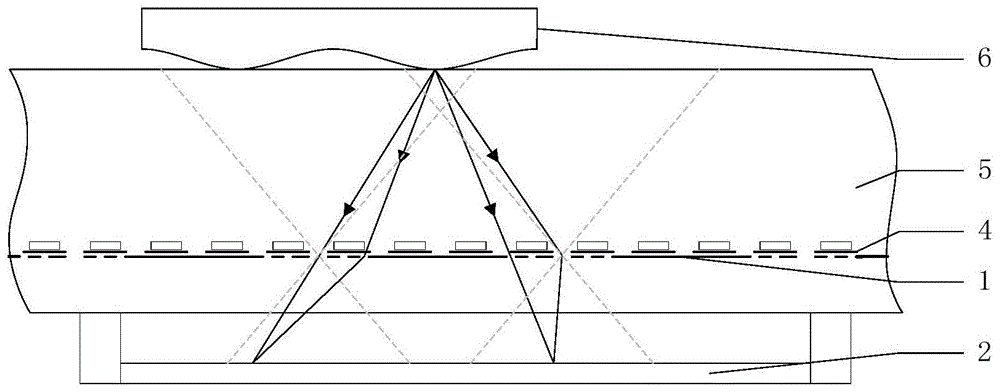
图3为本申请的成像装置的一种实现方式中,汇聚光线的光路示意图;3 is a schematic diagram of an optical path of converging light in an implementation manner of the imaging device of the present application;
图4为本申请的成像装置的一种实现方式中,成像层的俯视图;4 is a top view of an imaging layer in an implementation manner of the imaging device of the present application;
图5为本申请的一种电路层的俯视图;5 is a top view of a circuit layer of the application;
图6为本申请的成像装置应用在具有显示屏的电子设备中的一种实现方式的结构示意图;6 is a schematic structural diagram of an implementation manner in which the imaging device of the present application is applied to an electronic device with a display screen;
图7A为本申请的另一种电路层的俯视图;7A is a top view of another circuit layer of the application;
图7B为本申请的另一种电路层的俯视图;7B is a top view of another circuit layer of the application;
图8A为本申请对应图7A电路层的成像层的俯视图;8A is a top view of the imaging layer corresponding to the circuit layer of FIG. 7A in the present application;
图8B为本申请对应图7B电路层的成像层的俯视图;FIG. 8B is a top view of the imaging layer corresponding to the circuit layer of FIG. 7B in the present application;
图9为本申请对应图5电路层的成像层的俯视图;9 is a top view of the imaging layer corresponding to the circuit layer of FIG. 5 in the present application;
图10A为本申请的成像装置应用在具有显示屏的电子设备中的另一种实现方式的结构示意图;10A is a schematic structural diagram of another implementation manner in which the imaging device of the present application is applied to an electronic device with a display screen;
图10B为本申请的成像装置应用在具有显示屏的电子设备中的另一种实现方式的结构示意图;10B is a schematic structural diagram of another implementation manner in which the imaging device of the present application is applied to an electronic device with a display screen;
图11为本申请减少单位面积内的发光像素数量后,成像装置应用在具有显示屏的电子设备中的另一种实现方式的结构示意图;11 is a schematic structural diagram of another implementation manner in which the imaging device is applied to an electronic device with a display screen after the number of light-emitting pixels per unit area is reduced in the present application;
图12为根据图11对应成像层的俯视图;FIG. 12 is a top view of the corresponding imaging layer according to FIG. 11;
图13本申请的成像装置应用在具有显示屏的电子设备中的另一种实现方式的结构示意图;13 is a schematic structural diagram of another implementation manner in which the imaging device of the present application is applied to an electronic device with a display screen;
图14A本申请的成像装置应用在具有显示屏的电子设备中的另一种实现方式的结构示意图;14A is a schematic structural diagram of another implementation manner in which the imaging device of the present application is applied to an electronic device with a display screen;
图14B本申请的成像装置应用在具有显示屏的电子设备中的另一种实现方式的结构示意图;14B is a schematic structural diagram of another implementation manner in which the imaging device of the present application is applied to an electronic device with a display screen;
图15本申请的倾斜的波带片结构的一种结构示意图;15 is a schematic structural diagram of the inclined zone plate structure of the present application;
图16本申请的倾斜的波带片结构的另一种结构示意图;FIG. 16 is another structural schematic diagram of the inclined zone plate structure of the present application;
图17本申请的倾斜的波带片结构的设计原理图;17 is a schematic diagram of the design of the inclined zone plate structure of the present application;
图18本申请的倾斜的波带片结构应用在指纹采集装置中的一种实现方式的结构示意图;18 is a schematic structural diagram of an implementation manner in which the inclined zone plate structure of the present application is applied to a fingerprint acquisition device;
图19为本申请的倾斜的波带片结构应用在指纹采集装置中的光路示意图;19 is a schematic diagram of the optical path of the application of the inclined zone plate structure of the present application in a fingerprint collection device;
图20为本申请的波带片结构应用在感光像元的一种实现方式的结构示意图。FIG. 20 is a schematic structural diagram of an implementation manner in which the zone plate structure of the present application is applied to a photosensitive pixel.
图21为本申请的具有双层成像层的一种实现方式的光路示意图;21 is a schematic diagram of an optical path of an implementation with a double-layer imaging layer of the present application;
图22为本申请的具有双层成像层的另一种实现方式的光路示意图。FIG. 22 is a schematic diagram of an optical path of another implementation manner of the present application having a double-layer imaging layer.
具体实施方式Detailed ways
矩阵式多孔成像(MAPIS,MAtrix Pinhole Image Sensing)装置,可以用在超薄式光学指纹采集、显示屏上的指纹采集(FOD,Fingerprinting On Display)等场合。Matrix Pinhole Image Sensing (MAPIS, MAtrix Pinhole Image Sensing) device can be used in ultra-thin optical fingerprint collection, fingerprint collection on display (FOD, Fingerprinting On Display) and other occasions.
参照图1和图2,图1为MAPIS的成像光路图,图2为MAPIS小孔板的俯视图,MAPIS一般包括小孔板101和图像传感器102。在小孔板101上开设有多个成像孔。图像传感器102设置在小孔板101的一侧,并且与成像孔的位置对应。这样,根据小孔成像原理,小孔板101另一侧的目标物上的光线,就可以穿过成像孔,在图像传感器102上形成目标物的倒立的像。穿过每一个成像孔的光线都可以在图像传感器102上形成一个相应的像,将这多个像进行拼接,就可以得到一个相对完整的关于目标物的图像。Referring to FIGS. 1 and 2 , FIG. 1 is an imaging optical path diagram of MAPIS, and FIG. 2 is a top view of a MAPIS orifice plate. MAPIS generally includes a
但MAPIS技术存在如下一些缺点。例如:1.对于直径5微米的小孔,根据艾里斑计算公式,对0.55μm的绿光,在400微米的距离上,艾里斑直径=1.22*400*0.55/5=53.68微米。可见通过5微米的小孔的光其衍射斑扩大了大约10倍,面积相应的扩大了一百倍,从而光强减弱了一百倍,这对成像是很不利的。如果是高分辨率的显示屏,小孔的直径可能会进一步缩小,从而衍射更加严重,能量急剧衰减。因此,小孔孔径过大时导致图像模糊,小孔孔径较小时能量不足,同时导致能量不足和图像模糊。2.一些场合限制使用合适尺寸的小孔。例如,将MAPIS技术应用于OLED显示屏内时,受OLED显示屏内驱动电路线路限制,只能在电路网的透光间隙放置成像小孔,不能自由调整小孔的形状和尺寸,使小孔成像能量不足,性能下降。However, MAPIS technology has the following shortcomings. For example: 1. For a hole with a diameter of 5 microns, according to the Airy disk calculation formula, for a green light of 0.55 μm, at a distance of 400 microns, the diameter of the Airy disk=1.22*400*0.55/5=53.68 microns. It can be seen that the diffraction spot of the light passing through the 5-micron hole is enlarged by about 10 times, and the area is correspondingly enlarged by a hundred times, so that the light intensity is weakened by a hundred times, which is very unfavorable for imaging. If it is a high-resolution display, the diameter of the small hole may be further reduced, resulting in more serious diffraction and sharp attenuation of energy. Therefore, when the aperture is too large, the image is blurred, and when the aperture is small, the energy is insufficient, resulting in insufficient energy and blurred image. 2. Some occasions restrict the use of small holes of suitable size. For example, when the MAPIS technology is applied in the OLED display screen, due to the limitation of the driving circuit in the OLED display screen, the imaging holes can only be placed in the light transmission gap of the circuit net, and the shape and size of the small holes cannot be adjusted freely to make the small holes Imaging power is insufficient and performance is degraded.
另一方面,即使可以开很大的孔,光强也可能不足。这是因为虽然随着孔的增大,透过的光总量增加了,但是形成的光斑也增大了,从而单位面积上的光强并没有增大。On the other hand, even if a very large hole can be made, the light intensity may not be sufficient. This is because although the total amount of transmitted light increases with the increase of the aperture, the formed light spot also increases, so the light intensity per unit area does not increase.
为了解决这一问题,在本申请提出可以应用到电子设备中的一种成像装置,尤其是具有显示屏的电子设备中,可以用来对接触显示屏的目标物成像或者对显示屏外的目标物进行成像,能够充分利用光的干涉增强特性。接触显示屏的目标物可以是指纹、掌纹等。In order to solve this problem, this application proposes an imaging device that can be applied to electronic equipment, especially electronic equipment with a display screen, which can be used to image a target touching the display screen or to image a target outside the display screen. It can make full use of the interference-enhancing properties of light. The objects that touch the display screen can be fingerprints, palm prints, etc.
显示屏内包括电路层4,通常电路层4是层叠交错设计排布的,很难设计出足够大的小孔,但是可以设计出许多较小的小孔,如图5所示,图5中,白色区域为电路层4的透光小孔,光线透过这些小孔后会相互干涉,形成复杂的干涉条纹,难以处理。在过去的方案中,可以选择这些小孔中最大的一个,并且屏蔽其他的小孔。这样虽然降低了干扰,但同时也降低了光强。The display screen includes a
仔细分析小孔之间的相干干涉,发现,对像面上的某一点来说,一般来说,总有一部分小孔的干涉是相干增强的,另一部分的小孔的干涉是相干相消的。从光程的角度分析,暂不考虑光源到小孔的光程,一部分小孔到像面上某点的光程之间的差是波长的整数倍,那通过这些小孔的光在像面上是相干增强的;通过另一部分小孔的光走过的光程与通过前述这些小孔的光的光程差是波长的半整数倍,即0.5倍,1.5倍,2.5倍等的时候,那相对于前述这些小孔,这部分光程差是波长的半整数倍的光线是相干相消的。从而,可以设置一层成像层1,将这些相干相消的小孔遮挡,只留下相干增强的小孔,这样在像面上的该点,光线全都是相干增强的,从而光强会大大增强。由此在成像层1上形成由遮光带和透光带组成的波带片结构。由于是相干叠加,光波的振幅是直接叠加的,而光的强度正比于振幅的平方,从而最终该点光的强度会正比于保留下的小孔数的平方。例如,如果保留了10个小孔,那该点光强会是只保留一个小孔时的一百倍,这样就大大增加了光强。基于上述分析,在本申请的第一个实施例中,一种电子设备用于对接触显示屏5的目标物成像,如:通过显示屏5进行指纹采集的指纹采集装置,参见图6,所述的电子设备包括:显示屏5和成像装置,所述成像装置包括成像层1和图像传感器2,所述成像层1位于所述图像传感器2上方。Carefully analyze the coherent interference between the small holes and find that, for a certain point on the image plane, generally speaking, the interference of some small holes is coherently enhanced, and the interference of another part of the small holes is coherently destructive . From the perspective of the optical path, the optical path from the light source to the small hole is not considered for the time being. The difference between the optical path from some small holes to a certain point on the image plane is an integer multiple of the wavelength. It is coherent enhancement; when the optical path difference of the light passing through another part of the small holes and the light passing through the aforementioned small holes is a half-integer multiple of the wavelength, that is, 0.5 times, 1.5 times, 2.5 times, etc., Compared with the aforementioned small holes, this part of the light whose optical path difference is a half-integer multiple of the wavelength is coherent and destructive. Therefore, a layer of
本实施中,成像层1为周期性成像板结构,上面周期性的设有多个遮光和透光部分。该周期可以与像素周期一致。In this embodiment, the
显示屏5可以包括发光像素层和电路层4,成像层1紧贴在电路层4的下侧或上侧,或者,所述成像层1由电路层4本身的电路线排布构成。当将成像装置应用到具有显示屏5的电子设备中时,显示屏5中的电路层4可以与以往的排布情况相同或者类似,此时,电路层4中仍然存在有间隙。光线可以通过这些间隙,故而这些间隙也可以统称为电路层4的透光部分。通常电路层4是层叠交错设计排布的,因此透光部分也通常是不规则的形状,为此,成像层1上设置与透光部分相配合的波带片结构3。The
所述的波带片结构3包括间隔设置的遮光带和透光带,波带片结构3是根据光干涉的原理计算设计得到,使得通过波带片结构3的光线总体的作用是增强的。例如,成像层1上的一个成像孔内设有的一个波带片结构3包括两个透光带和一个遮光带,当两个透光带的面积大于一个遮光带的面积时,可以取消对遮光带的遮挡,因为即使将遮光带取消,通过该成像孔的总体效果还是相干增强的。The
为了使效果达到最佳,可以将计算得到的所有相干增强的部分保留,形成透光带,将所有相干相消的部分遮挡,形成遮光带。使得经过透光带的单色光相干增强汇聚于图像传感器上,而对于遮光带部分为经过计算单色光相干相消汇聚与于图像传感器上的部分,进而使得汇聚在图像传感器上的光均为相干增强光线,极大的放大了光强。In order to achieve the best effect, all the coherently enhanced parts obtained by calculation can be retained to form a light-transmitting band, and all the coherently canceled parts can be blocked to form a light-shielding band. The coherent enhancement of the monochromatic light passing through the light-transmitting belt is concentrated on the image sensor, and the part of the shading belt is the part of the image sensor after the calculation of the coherent and destructive coherence of the monochromatic light, so that the light converging on the image sensor is uniform. To coherently enhance the light, the light intensity is greatly amplified.
由于本申请技术方案利用了光的衍射/干涉等波动特性,而光的波动性是和光的波长相关的,从而在进行指纹采集时,显示屏5发出单色光,单色光通过与显示屏5接触的手指6反射后分别经过电路层4的透光部分和成像层1的透光带后,由于光的衍射和光的干涉汇聚在图像传感器上成像,单色光可以是绿光、红光和蓝光中的任一种色光。设计波带片结构时,根据单色光的颜色不同,对应的波带片结构3的遮光带和透光带的位置不同。采用单色光照明,并且波带片结构3只对某一单色光具有汇聚作用,是一个巨大的优势。这意味着其他波长的外界干扰光无法汇聚,从而降低了背景噪声。另一方面,OLED屏幕本身发光就是由单色光混合而成,从而让屏幕发出单色光非常的容易实现。Since the technical solution of the present application utilizes the wave characteristics such as diffraction/interference of light, and the wave characteristic of light is related to the wavelength of light, the
显示屏5是有一定透光能力的显示屏,如OLED屏。在显示屏5上设有指纹采集区域,在指纹采集区域下方对应有若干个发光像素,在与每个发光像素对应的电路层4上都有若干个透光部分,在一种可实现方式中,每个发光像素对应的透光部分下面均设置一个能够将相干增强的光线汇聚在图像传感器上的波带片结构3,在另一种可实现方式中,多个发光像素对应的透光部分下面均设置一个能够将相干增强的光线汇聚在图像传感器上的波带片结构3,这样使得在使用该电子设备采集指纹时,手指接触显示屏5指纹采集区域后,射入到图像传感器上的光都是相干增强部分的光线,极大的放大的光线的亮度,使得采集的指纹图像亮度更高,更加清晰。The
现有技术中,显示屏5的指纹采集是利用小孔成像的原理,根据指纹的特性,即指纹包括脊的部分和谷的部分,当手指与显示屏5接触时,脊的部分与显示屏5直接接触,谷的部分与显示屏5之间留有空隙,根据光线在不同介质中的折射率/反射率不同,故而在图像传感器上形成明暗相间的条纹,但是由于只有一个小孔能够透光,在图像传感器上形成的亮条纹和暗条纹整体都比较暗,与现有技术相比,本申请中利用了绝大部分的透光部分,保证了进光量,同时波带片结构3的设计保证了射入的光线总体是相加相关光线,极大的放大的光线的亮度,使得采集的指纹图像亮度更高,更加清晰。同时,由于增加了透光面积,由光的波动性产生的干涉/衍射的次峰的相对高度和其与主峰之间的距离也会降低。从而进一步提高了光学分辨率。In the prior art, the fingerprint collection of the
在传统光学中,菲涅尔波带片被视为一个透镜,具有焦距和景深。对于一个固定的物,像面在一定距离范围内才能成像;对于一个固定的像面,物在一定范围内才能将像落在该像面上。在屏下指纹检测场景中,物距是固定的,从而像距也是固定的,且成的像应该落于传感器上。然而,由于配装的精度限制,图像传感器往往不能准确的位于像面上,而是有一定误差。这时候,就需要有比较大的景深,来允许这个误差。如果将波带片结构设置成仅有一环或较小的数环,则可以有较大的景深来允许这个误差。一般来说,在本申请中,可以认为景深=焦距/波带数。In conventional optics, a Fresnel zone plate is viewed as a lens with a focal length and depth of field. For a fixed object, the image surface can only be imaged within a certain distance range; for a fixed image surface, the object can only place the image on the image surface within a certain range. In the under-screen fingerprint detection scene, the object distance is fixed, so the image distance is also fixed, and the formed image should fall on the sensor. However, due to the limitation of assembly precision, the image sensor often cannot be located on the image plane accurately, but has a certain error. At this time, a relatively large depth of field is required to allow for this error. If the zone plate structure is set to have only one ring or a smaller number of rings, there can be a larger depth of field to allow for this error. Generally, in this application, it can be considered that depth of field = focal length/number of wavebands.
成像层1设置在图像传感器之上,成像层1位于电路层4上方或下方,电路层4包括多层用于驱动发光像素的电路,多层所述电路层4中的电路交错层叠,交错的电路层4上有多个透光部分,透光部分可能是规则的形状也可能是不规则的形状,在实际应用时,其中,多个透光部分可能是如图7A和图7B所示的情况,包括几个比较大的透光部分,为了方便描述,将比较大的透光部分称为第一透光部分,第一透光部分是指在该透光部分足够设置至少一个波带片结构3;多个透光部分还可能是如图5所示的情况,所有的透光部分的面积都相对比较小,为了方便描述,将比较小的透光部分称为第二透光部分,第二透光部分是指在该透光部分不足以设置多条波带。针对图7A和图7B所示的情况,选取其中面积比较大几个透光部分(第一透光部分),在选取的第一透光部分下面对应的成像层1位置上设置对应波带片结构3。参见图8A和图8B,成像层1上设有若干个波带片结构3,每个波带片结构3分别与对应的第一透光部分相互配合。需要说明的是,这种情况下的波带片结构只是露出一部分,设置在第一透光部分的波带片结构3是指包括间隔设置遮光带和透光带的结构,其相对一个完整的同心环结构来说,波带片结构3相当于一个完整的同心环结构中的一部分(参见图8A和图8B)。不同形状的第一透光部分对应的波带片结构3不同。每个波带片结构3都是根据光的干涉的原理计算设计得到,使得依此经过第一透光部分和透光带的单色光相干增强汇聚于图像传感器上,极大的放大了光强。针对上述情况对应的波带片结构3,可以理解为先在选取的第一透光部分下面对应的成像层1位置上设置同样形状,同样大小的成像孔,然后根据射入成像孔的单色光的波长计算光线通过成像孔到图像传感器2上某一点的光程,计算得到相干增强干涉光和相干相消干涉光,其中,在相干增强部分保留透光的设置,将相干相消部分遮挡起来形成遮挡带,这样使得射入图像传感器的光线都是相干相加的效果,极大的放大了光强。另一方面,由于加工精度的关系,过于细小的波带片结构可能难以实现,所以当所述波带片结构中透光带的面积总和大于遮光带的面积总和时,可以将所述遮光带去除,同样能够保证通过该成像孔的光线总体是增强的效果。这样虽然一定程度上降低了光强,但是加工起来更容易,而且也比遮掉该成像孔光强更强。The
进一步的,波带片结构3是有焦距的,其焦距为
针对如图5所示的情况,第二透光部分的面积都比较小,每个第二透光部分都不足以对应设置多条波带(间隔的遮光带和透光带),因此,可以在成像层1上设计一个完整的波带片结构3,完整的波带片结构3是指包括一系列同心环的结构,同心环是指包括间隔设置的闭环遮光带和闭环透光带,如图9所示,将完整的波带片结构3与电路层4的第二透光部分对齐,对齐的准则是使所述成像层的透光带与所述电路层的第二透光部分重合,优选的,电路层4的第二透光部分与波带片结构3的透光带重合面积满足预设面积阈值范围,或有最大的重合面积,使透光率达到最高。For the situation shown in FIG. 5 , the area of the second light-transmitting parts is relatively small, and each second light-transmitting part is not enough to set a plurality of wavelength bands (spaced light-shielding bands and light-transmitting bands). Therefore, it is possible to A complete
进一步的,发光像素层包括阵列排布的发光像素。发光像素层的下方设置有电路层4,电路层4包括多层电路,其中包括用于驱动和控制发光像素的电路。此外,电路层4中还可以包括用于其他用途的电路。其中,发光像素由于涂抹有有机发光材料等,本身是不透光的,在各个发光像素之间是留有缝隙,而在缝隙对应的电路层4上存在透光部分,所以透光部分是存在发光像素周围的,基于此,本申请中的波带片结构3可以是对应于发光像素的外圈的电路层4的透光部分,相当于抛弃了中间的几环,而保留外面的一环或几环,其中,抛弃的部分的直径与发光像素的直径对应。Further, the light-emitting pixel layer includes light-emitting pixels arranged in an array. A
例如,一个像素周期是70μm,其中不透光的中心部分大约是40μm直径,那么就可以在不透光部分之外的40至70μm区域设置一环或多环透光区域。For example, if one pixel period is 70 μm, and the opaque central portion is about 40 μm in diameter, then one ring or multiple rings of light transmitting regions can be provided in the 40 to 70 μm region outside the opaque portion.
另一方面,现有的波带片设计是整数环,但在我们的方案中,并非一定需要从整数环开始。举个例子,比如像素周期是70μm,其中不透光的中心部分大约是40μm直径,但是根据光波波长和焦距设计出的波带片,第一圈直径是30μm,第二圈直径是42μm,没有恰好40μm的。但是根据公式计算,可以发现第1.9圈正好是40μm.这时候就可以保留第1.9圈至第2.9圈之间的透光部分,遮挡0至1.9圈之间的部分。这样也是一个完整的波带,具有相干增强的功能。并且,这样设计的波带,其透光面积比在电路内找透光面积更大。On the other hand, existing zone plate designs are integer rings, but in our scheme, it is not necessary to start with integer rings. For example, if the pixel period is 70μm, the central part of the opaque part is about 40μm in diameter, but the zone plate designed according to the wavelength and focal length of the light wave, the diameter of the first circle is 30μm, the diameter of the second circle is 42μm, no Exactly 40µm. However, according to the formula calculation, it can be found that the 1.9th circle is exactly 40 μm. At this time, the light-transmitting part between the 1.9th circle and the 2.9th circle can be reserved, and the part between 0 and 1.9th circle can be blocked. This is also a complete waveband with the function of coherence enhancement. Moreover, the light-transmitting area of the wavelength band designed in this way is larger than the light-transmitting area found in the circuit.
可以理解的是本申请中所提及的波带片结构3不是现有的圆形菲涅耳波带片,而是根据电路层4实际情况而设计的,为了便于描述,而命名为波带片结构3。It can be understood that the
还需要说明的是,可以一个所述波带片结构3对应一个发光像素像素,也可以一个所述波带片结构3对应多个发光像素。最终所有汇聚在图像传感器上的点合成一个完整的图像。但是,最好不要一个所述波带片结构3对应所有的发光像素,因为如果一个所述波带片结构3对应所有的发光像素,那么波带片结构3的外沿,每个带可能过细,从而无法加工。It should also be noted that one of the
还需要说明的是,所述成像孔和所述波带片结构的透光带除了可以用作光通路,还可以用作电路线走线的通孔。例如,可以充当上下层电路连接的通孔或者充当电路层与像素层连接的通孔,使得更有利于显示屏的设计。It should also be noted that, the imaging hole and the light-transmitting zone of the zone plate structure can be used not only as a light path, but also as a through hole for circuit wiring. For example, it can be used as a through hole for connecting the upper and lower layers of the circuit or as a through hole for connecting the circuit layer and the pixel layer, which is more conducive to the design of the display screen.
该指纹采集装置一方面利用了多个透光部分,增加了进光量,同时与现有技术中只选取一个透光部分进行小孔成像相比,利用了多个透光部分相当于透光区的等效直径变大了,从而使光的衍射现象变弱了;另一方面通过波带片结构3提高了光强,使光线很轻易被图像传感器接收,从而提高图像清晰度和分辨率。On the one hand, the fingerprint collecting device utilizes a plurality of light-transmitting parts to increase the amount of light entering, and at the same time, compared with the prior art where only one light-transmitting part is selected for pinhole imaging, the use of a plurality of light-transmitting parts is equivalent to a light-transmitting area. On the other hand, the light intensity is increased through the
在本申请的第二个实施例中,用于对显示屏外的目标物成像的电子设备,提供充当摄像头,尤其是前置摄像头的功能。In the second embodiment of the present application, the electronic device for imaging the target outside the display screen provides the function of serving as a camera, especially a front camera.
现有的电子设备,如智能手机、平板电脑等都包括前置摄像头和后置摄像头,前置摄像头包括设置在显示屏上的镜光孔和位于镜光孔后面的图像传感器,目标物通过镜头生成的光学图像投射到图像传感器表面上,前置摄像头主要用于自拍和视频通话时使用。也就是说前置摄像头需要在显示屏上开孔,这也是导致现有的电子设备无法实现真正意义上的全面屏的原因。Existing electronic devices, such as smart phones, tablet computers, etc., all include a front camera and a rear camera. The front camera includes a mirror aperture set on the display screen and an image sensor behind the mirror aperture, and the target passes through the lens. The resulting optical image is projected onto the image sensor surface, and the front-facing camera is primarily used for selfies and video calls. That is to say, the front camera needs to open a hole on the display screen, which is also the reason why the existing electronic equipment cannot achieve a full screen in the true sense.
本申请提出一种设置在显示屏下的图像采集装置,应用在具有显示屏的电子设备上,用来采集显示屏外目标物的图像,能够解决现有技术中由于前置摄像头的设置,无法实现全面屏的问题。The present application proposes an image acquisition device disposed under a display screen, which is applied to an electronic device with a display screen and is used to collect images of objects outside the display screen, which can solve the problem of inability to be installed in the prior art due to the setting of the front camera. The problem of realizing full screen.
首先需要说明的是,人眼所能感受到的自然界中所有的颜色都可以用红、绿、蓝这三种颜色波长的不同强度组合而得,这就是三基色原理。First of all, it should be noted that all the colors in nature that can be perceived by the human eye can be obtained by combining the different intensities of the three color wavelengths of red, green and blue. This is the principle of three primary colors.
本申请提出的一种设置在显示屏下的图像采集装置,参见图10A和图10B,包括电路层4、成像层1和三个图像传感器,其中所述的三个图像传感器为分别用于接收红光的图像传感器201、接收绿光的图像传感器202和接收蓝光的图像传感器203,三个图像传感器对应的成像层1上设有三种波带片结构3,三种波带片结构3分别根据光线为红光、绿光和蓝光设计得到。对显示屏5外的目标物成像时,目标物发射的光线经过电路层4的透光部分、成像层1的透光带,分别落在三个图像传感器上,最终将三个图像传感器上的图像处理成一个完成的彩色图像。An image acquisition device provided under the display screen proposed in the present application, referring to FIG. 10A and FIG. 10B , includes a
本申请的第二个实施例是基于第一个实施例的原理而设计,其三种波带片结构3的设计原理不在赘述。The second embodiment of the present application is designed based on the principle of the first embodiment, and the design principles of the three types of
进一步的,为了提高成像质量,参见图11和图12,在一种可实现方式中,可以在显示屏的显示区的部分区域实现低分辨率显示,具体的可以减少单位面积内的发光像素数量;例如,在显示屏上选择一个或几个不是很重要的发光像素点,比如,在显示电量的位置减少一个发光像素,从而在该发光像素对应的位置可以露出较完整的成像孔,从而可以在该成像孔位置设置一个相对完整的波带片结构3,在另一种可实现方式中,可以通过电路层4的电路避让,增大透光部分的面积。进一步的,为了减小对显示效果的影响,间隔着去掉几个发光像素,即相邻两个缺失的发光像素之间间隔有至少一个发光像素,对应的可以一个波带片覆盖这几个去掉发光像素后留下的透光部分,从而大大增加光强。Further, in order to improve the imaging quality, referring to FIG. 11 and FIG. 12 , in an implementation manner, low-resolution display can be realized in part of the display area of the display screen, and specifically, the number of light-emitting pixels per unit area can be reduced. ; For example, select one or several light-emitting pixels that are not very important on the display screen, for example, reduce a light-emitting pixel at the position where the power is displayed, so that a relatively complete imaging hole can be exposed at the corresponding position of the light-emitting pixel, so that it can be A relatively complete
进一步,选择同一颜色的发光像素去除,也就是说,所有的缺失的发光像素均为同一颜色的发光像素。例如,显示电量时,如果只需要绿色和红色,那么可以在显示电量位置将蓝色发光像素去除。Further, the light-emitting pixels of the same color are selected to be removed, that is, all the missing light-emitting pixels are light-emitting pixels of the same color. For example, when displaying the power, if only green and red are needed, the blue light-emitting pixels can be removed from the position where the power is displayed.
与上述两种可实现方式相配合的成像装置,包括成像层1和图像传感器2。请参见图3,成像层1包括若干个成像孔,每个所述的成像孔内设有一个波带片结构3,如图4所示,所述的波带片结构3包括间隔设置的遮光带和透光带,每个波带片结构3都是根据光干涉的原理计算设计得到,使得经过透光带的单色光相干增强汇聚于图像传感器上,而对于遮光带部分为经过计算单色光相干相消汇聚于图像传感器上的部分,进而使得汇聚在图像传感器上的光为相干增强光线,极大的放大了光强。在成像时,每个波带片结构3将产生一个像斑,将多个像斑拼接起来,可以得到完整的目标图像。拼接的过程包括倒像纠正、亮度校正、拼接等步骤。The imaging device cooperating with the above two achievable manners includes an
与现有的MAPIS成像相比,MAPIS成像利用的小孔成像,是自由衍射成像,本申请中通过波带片结构3汇聚光线成像。因此在相同孔径下,本申请的成像装置有更高的分辨率,在像点有更高的能量。这是由于波带片结构3消除了相位相反的光波互相抵消,因此大大增强了汇聚点的能量。在波带片结构3内有20个半波带时,像点的能量是小孔的自由衍射时的400倍左右。另外,小孔成像不能使用较大的孔径,否则图像模糊;而本申请的成像装置成像时,因为它类似于薄透镜的汇聚光线作用,所以可以使用很大的孔径,不必担心图像模糊,大孔径还可以进一步增加透光率,增强成像的能量。Compared with the existing MAPIS imaging, the pinhole imaging used in the MAPIS imaging is free diffraction imaging, and in this application, the light is converging through the
上述两种可实现方式,可以使成像孔可汇聚更大的光能量进行成像。同时,对较远目标物成像时,目标物表面上的每一点,会通过成像孔在图像传感器上形成多个有视差的像点,从而可基于多个像点计算其深度信息,或进行噪声滤除或分辨率增强。例如,假设成像孔的周期为0.5mm,即每0.5mm设置一个成像孔,并使用5mm*5mm的图像传感器,则一次成像,可以得到100个像斑。对于30mm以上的远方目标物,它在这100个像斑内都有像。从而,我们可以基于这100个像斑进行充分的信号处理计算,消除噪声、提升分辨率或者计算准确的深度信息。The above two achievable manners can enable the imaging hole to concentrate more light energy for imaging. At the same time, when imaging a distant target, each point on the surface of the target will form multiple image points with parallax on the image sensor through the imaging hole, so that its depth information can be calculated based on multiple image points, or noise can be calculated. Filter out or resolution enhancement. For example, assuming that the period of the imaging holes is 0.5mm, that is, one imaging hole is set every 0.5mm, and an image sensor of 5mm*5mm is used, then 100 image spots can be obtained for one imaging. For distant objects above 30mm, it has images in these 100 image spots. Therefore, we can perform sufficient signal processing calculations based on these 100 image spots to remove noise, improve resolution, or calculate accurate depth information.
本实施例中,显示屏上没有肉眼可见的孔,也不会对显示产生严重影响,可以真正的实现全面屏。另外,由于没有透镜,厚度也可以大为降低,更易于安装于显示屏之下。In this embodiment, there is no hole visible to the naked eye on the display screen, and it will not have a serious impact on the display, and a full screen can be truly realized. In addition, since there is no lens, the thickness can also be greatly reduced, making it easier to install under the display screen.
为了进一步降低光的衍射现象,优选将电路层4与成像层1之间的距离尽可能缩短,如第一实施例和第二实施例中,将成像层1紧贴于电路层4。In order to further reduce the diffraction phenomenon of light, it is preferable to shorten the distance between the
为了实现这一目标,可以采用光刻技术,光刻技术是利用光学-化学反应原理和化学、物理刻蚀方法,将电路图形传递到单晶表面或介质层上,形成有效图形窗口或功能图形的工艺技术。具体的,在光照作用下,借助光致抗蚀剂(又名光刻胶)将掩膜版上的图形转移到基片上。其主要过程为:首先紫外光通过掩膜版照射到附有一层光刻胶薄膜的基片表面,引起曝光区域的光刻胶发生化学反应;再通过显影技术溶解去除曝光区域或未曝光区域的光刻胶(前者称正性光刻胶,后者称负性光刻胶),使掩膜版上的图形被复制到光刻胶薄膜上;最后利用刻蚀技术将图形转移到基片上。In order to achieve this goal, photolithography technology can be used. Photolithography technology uses the principle of optical-chemical reaction and chemical and physical etching methods to transfer the circuit pattern to the single crystal surface or dielectric layer to form an effective pattern window or functional pattern. process technology. Specifically, under the action of light, the pattern on the mask is transferred to the substrate by means of a photoresist (also known as photoresist). The main process is: first, ultraviolet light is irradiated to the surface of the substrate with a layer of photoresist film through the mask, causing a chemical reaction of the photoresist in the exposed area; Photoresist (the former is called positive photoresist, the latter is called negative photoresist), so that the pattern on the mask is copied to the photoresist film; finally, the pattern is transferred to the substrate by etching technology.
很显然,采用光刻技术不可避免的需要使用掩膜版,申请人考虑到,如果生产商使用光刻技术将电路层4与成像层1同时生产,那就需要根据本申请的成像装置重新设计一套掩膜版,然而掩膜版的价格十分昂贵,为了解决这一难题,本申请提出将成像层1固定在图像传感器上。Obviously, the use of photolithography technology inevitably requires the use of a mask. The applicant considers that if the manufacturer uses photolithography technology to produce the
如图13所示的用于对接触显示屏的目标物成像的电子设备,其绝大部分与第一个实施例相同,不同之处在于:在图像传感器2上设有透明玻璃层7,在透明玻璃层7上表面设置成像层1,成像层1上的波带片结构3与上方电路层4的透光部分对应。As shown in FIG. 13, most of the electronic equipment used for imaging the target contacting the display screen is the same as the first embodiment, the difference is: the
类似的,如图14A和图14B所示的用于对显示屏外的目标物成像的电子设备,其绝大部分与第二个实施例相同,不同之处在于:在每个图像传感器上都设有透明玻璃层7,在透明玻璃层7上表面设置成像层1,成像层1上的波带片结构3与上方电路层4的透光部分对应。Similarly, most of the electronic equipment for imaging the target outside the display screen as shown in FIG. 14A and FIG. 14B is the same as the second embodiment, the difference is that each image sensor has A
成像层1通过透明玻璃固定在图像传感器上,通过调整透明玻璃的厚度来调整电路网与成像层1之间的距离,在生产时,将生产好的成像装置直接贴合在显示屏下即可。透明玻璃不影响光线在图像传感器上的汇聚,同时大大的降低了生产成本。The
另外,对于波带片结构的外沿,每个带可能过细从而无法加工的情况下。通过将成像层1设在图像传感器2上设有透明玻璃层7上表面的方式,更容易加工。Also, for the outer edge of the zone plate structure, each zone may be too thin to be machined. By providing the
本申请上述实施例中的成像层1均为成像板结构,设置在电路层4上方或下方。本申请提出成像层1的另一种可实现的方式,利用电路层4本身,在设计电路的时候,将电路层4错综复杂的电路线设计成包括透光部分和遮光部分的构造,例如,在需要透光的部分,将电路设置成稀疏甚至是透明的,在不需要透光的部分,将电路设置成密集的不透光的。其中,透光部分和遮光部分起到波带片结构的作用,即电路层本身就可以视为波带片结构。透光部分为光线的相干增强部分,遮光部分为光线的相干相消部分,使光线穿过电路层4的透光部分后汇聚在图像传感器上。The
另外,所述成像层可以采用导电材料制成,成像层相当于一个大面积的导体,可以用来供电,与通过电线供电相比,其电阻更小、电压更稳定。当成像层设置在显示屏里时,显示屏里的各个需要供电的部件,比如发光像素,距离传感器,环境光传感器等,都可以从成像层取电。In addition, the imaging layer can be made of conductive material. The imaging layer is equivalent to a large-area conductor, which can be used for power supply. Compared with power supply through wires, its resistance is smaller and the voltage is more stable. When the imaging layer is arranged in the display screen, each component in the display screen that needs to be powered, such as light-emitting pixels, distance sensors, ambient light sensors, etc., can take power from the imaging layer.
进一步地,当需要供电时,可以将各条遮光带之间通过连接件连通,以保证整体等电压,所述连接件采用导电材料制成。例如,可以通过若干个连接条将各条遮光带连接起来。Further, when power supply is required, the shading strips can be connected through connecting pieces to ensure the overall equal voltage, and the connecting pieces are made of conductive materials. For example, the shading strips can be connected by several connecting strips.
对于波带片结构3可以选用多种不同的样式,例如偶数带遮挡的波带片、奇数带遮挡的波带片、圆环形波带片、矩形栅格波带片等,或其他特殊设计的波带片,以适应不同成像条件的需要。For the
进一步的,本申请公开一种倾斜的波带片结构,以将其用于倾斜角度光线的成像,参见图15和图16,图15和图16分别提供了适合两种不同倾斜角度光线成像的倾斜的波带片结构。倾斜的波带片结构301的遮光带与透光带不是同心圆环,而是倾斜在一侧。Further, the present application discloses an inclined zone plate structure, which is used for imaging of light with inclined angles, see FIG. 15 and FIG. 16 , respectively. Tilt zone plate structure. The light-shielding zone and the light-transmitting zone of the inclined
参见图17,图17示出了如何获得所述的倾斜的波带片结构301的过程,首先,在入射光线的法面上(即入射平面波的波前)放置一个同心圆环的波带片结构,即正波带片结构302,与入射光轴正交;然后取正波带片结构302的焦平面与入射光光轴的交点,记为点F,它是正波带片结构302的焦点;最后以点F为中心,对正波带片结构302进行中心投影,落在衍射平面上的投影即是倾斜的波带片结构301。倾斜的波带片结构301对倾斜入射的光线有最佳的汇聚效果。Referring to Fig. 17, Fig. 17 shows the process of how to obtain the inclined
在一个具体例子中,参见图18,包括图像传感器2、倾斜波带片结构301和透明玻璃板8。如图19所示,本例子中倾斜波带片结构301的最佳成像角度θ为50°,透明玻璃板8折射率为1.5,则透明玻璃板8中的光线沿50°的方向向手指捺印面传播时,在玻璃-空气界面将发生全反射;而在玻璃-皮肤界面,全反射将被破坏,大部分光线将透射出透明玻璃板8。这样,反射的光线穿过倾斜波带片结构301,汇聚成像后,谷线-脊线将在输出图像上有很强的对比度。另一方面,外部的环境光由空气进入玻璃后,其角度将小于41.8°,不能经过倾斜波带片结构301很好地汇聚成像,从而降低了环境光噪声。In a specific example, referring to FIG. 18 , an
进一步地,倾斜波带片结构301的倾向角度应背离环境光的入射方向。例如,应用倾斜波带片结构的成像装置用于手机等可在室外移动的设备中时,其倾斜角度应当朝向显示屏下端,这是通常情况下背离太阳光的方向。Further, the inclination angle of the inclined
需要说明的是,本申请中所述的倾斜波带片结构的倾斜角度是指该倾斜波带片结构能够使入射光线达到最佳的汇聚效果的入射角,也就是说,倾斜角度与该入射光线的入射角相对应。It should be noted that the inclination angle of the inclined zone plate structure described in this application refers to the incident angle at which the inclined zone plate structure can make the incident light achieve the best convergence effect, that is, the inclination angle is related to the incident light. The incident angle of the light corresponds to.
本实施例中的倾斜波带片结构301可用于本申请中的其他所有实施例中。尤其是将倾斜波带片结构301应用在指纹采集中效果最佳,因为倾斜波带片结构倾斜的角度可以接受全反射的光线,其强度是正入射的6倍左右。The oblique
本申请还提供一种分视场成像装置,包括至少两个成像装置,每个成像装置包括波带片结构,波带片结构下方设有图像传感器,其中,每个波带片结构可以对应一个图像传感器,也可以多个波带片结构对应一个图像传感器;对应倾斜的视场光线配合使用倾斜波带片结构301,每个波带片结构用于将物方视场光线分别汇聚到对应的图像传感器上。通过将目标物分成多个分视场在对应成像装置上分别成像,最终通过图像处理将各个成像装置上获取的目标物部分图像拼接成一个完整的目标物图像。The present application also provides a split-field imaging device, including at least two imaging devices, each imaging device includes a zone plate structure, and an image sensor is arranged below the zone plate structure, wherein each zone plate structure may correspond to one The image sensor can also have multiple zone plate structures corresponding to one image sensor; the inclined
针对上述分视场成像装置,本申请还提供一种设备,包括显示屏和上述分视场成像装置,分视场成像装置对应设置在显示屏下方的透光部分。The present application further provides a device for the above-mentioned field-of-view imaging device, comprising a display screen and the above-mentioned field-of-view imaging device, where the sub-field-of-view imaging device is correspondingly disposed on a light-transmitting portion below the display screen.
图像采集器中用于接收光信号的最小单位为感光像元(又称感光像素,像素,pixel),图像采集器中通常设置若干感光像元。市面上图像采集器使用的感光像元都具有较宽的视场角。感光像元的视场角是指感光像元能响应的不同方向的入射光线所形成的最大角度。使用现有图像采集器直接进行成像时,视场角较大,往往得到的图像不清晰。为此本申请进一步提供一种窄视场感光像元。The smallest unit used to receive light signals in the image collector is a photosensitive pixel (also known as a photosensitive pixel, pixel, pixel), and a number of photosensitive pixels are usually set in the image collector. The photosensitive pixels used by image collectors on the market all have a wide field of view. The field of view of the photosensitive pixel refers to the maximum angle formed by the incident light in different directions that the photosensitive pixel can respond to. When the existing image acquisition device is used for direct imaging, the field of view is large, and the resulting image is often unclear. To this end, the present application further provides a narrow-field photosensitive pixel.
如图20所示,一种窄视场感光像元,包括光电转换单元,感光像元9,所述感光像元9上设置视场光阑10,所述视场光阑10即中间带有开孔的光阑,开孔部分能够透光,开孔外的部分不能透光,或者是在两个感光像元9之间设置遮光墙11,或者同时设置视场光阑10和遮光墙11。在感光像元9上方设置有波带片结构3,使得在设定视场之内的物点A,它发出的光线将通过波带片结构3汇聚在感光像元9的视场光阑10的小孔内,相应地,光电转换单元能够接收较高强度的光线,从而使物方视场内的图像能够清晰成像,产生有效输出;在设定视场之外的物点B,他发出的光线将通过波带片结构3,汇聚感光像元的视场光阑10的小孔之外,从而光电转换单元不能感受或只能以低强度感受到物方视场外的物点发出的光线,则物方视场外的图像便不能被获取或者获取的部分不会影响物方视场内的光线在光电转换单元上的成像,不能产生有效输出。从而可对感光像元的视场角进行限定,另外,遮光墙11的设置可以防止大角度光线的串扰。As shown in FIG. 20, a narrow field of view photosensitive pixel includes a photoelectric conversion unit, a
在上述实施例中,都采用一层波带片结构,一个波带片结构一般不会只对一个方向上的光线具有汇聚作用,而会对一个范围内的光线都具有汇聚作用,这有时是有害的。本申请基于以上实施例提供另一个实施例,本实施例中与上述实施例大部分相同,不同之处在于,采用双层波带片结构即,结构相同第一波带片和第二波带片,也就是在上述实施例中单层波带片结构的基础上再加一层完全相同的波带片结构,新加的一层波带片结构可以设置在原有波带片结构的上方或下方,两层的波带片结构的透光带可以完全对齐或者有一定的偏移,设置两个上下层叠的波带片结构,如图21和图22所示。这两个波带片结构的中心点之间的连线方向上的光线能够穿透这两个波带片并成像,其他方向的就不能了。在有些情况下,待测物体只在某个方向上光强特别强,比如导光板内全反射的情况。通过设置双层波带片结构,只接受某个方向上的光线,例如只接受由全反射产生的反射光线,可以大大增加光线强度,提高对比度。另一方面,当视场很小时,双层波带片结构可以起到当准直器的作用。In the above-mentioned embodiments, a single-layer zone plate structure is adopted. Generally, a zone plate structure does not only have a convergence effect on light in one direction, but also has a convergence effect on light in a range, which is sometimes harmful. The present application provides another embodiment based on the above embodiment. Most of this embodiment is the same as the above embodiment, except that a double-layer zone plate structure is adopted, that is, the first zone plate and the second zone plate have the same structure. In other words, on the basis of the single-layer zone plate structure in the above-mentioned embodiment, an identical layer of zone plate structure is added. Below, the light transmission bands of the two-layer zone plate structure can be completely aligned or have a certain offset, and two upper and lower zone plate structures are arranged, as shown in FIG. 21 and FIG. 22 . The light in the direction of the line between the center points of the two zone plate structures can penetrate the two zone plates and image them, but not in other directions. In some cases, the light intensity of the object to be measured is particularly strong only in a certain direction, such as the case of total internal reflection in the light guide plate. By setting up the double-layer zone plate structure, only receiving light in a certain direction, for example, only receiving the reflected light generated by total reflection, can greatly increase the light intensity and improve the contrast ratio. On the other hand, when the field of view is small, the dual-layer zone plate structure can act as a collimator.
在本申请的描述中,需要理解的是,术语“上”、“下”、“前”、“后”、“左”、“右”、“顶”、“底”、“内”、“外”等指示的方位或位置关系为基于附图所示的方位或位置关系,仅是为了便于简化描述,而不是指示或暗示所指的装置或元件必须具有特定的方位、以特定的方位构造和操作,因此不能理解为对本申请的限制。此外,在本申请的描述中,“多个”的含义是两个或两个以上。In the description of this application, it is to be understood that the terms "upper", "lower", "front", "rear", "left", "right", "top", "bottom", "inside", " The orientation or positional relationship indicated by "outside" is based on the orientation or positional relationship shown in the accompanying drawings, which is only for the convenience of simplifying the description, rather than indicating or implying that the referred device or element must have a specific orientation or be constructed in a specific orientation. and operation, and therefore should not be construed as a limitation on this application. In addition, in the description of the present application, "plurality" means two or more.
本说明书中各个实施例之间相同相似的部分互相参见即可。以上所述的本发明实施方式并不构成对本发明保护范围的限定。It is sufficient to refer to each other for the same and similar parts among the various embodiments in this specification. The embodiments of the present invention described above do not limit the protection scope of the present invention.
Claims (25)
Priority Applications (3)
| Application Number | Priority Date | Filing Date | Title |
|---|---|---|---|
| PCT/CN2020/077643 WO2020177689A1 (en) | 2019-03-05 | 2020-03-03 | Substrate structure, sensor module, electronic device and assembling method |
| PCT/CN2020/091306 WO2020233601A1 (en) | 2019-05-22 | 2020-05-20 | Imaging layer, imaging apparatus, electronic device, zone plate structure and photosensitive image element |
| TW109117160A TW202107065A (en) | 2019-05-22 | 2020-05-22 | Imaging layer, imaging apparatus, electronic device, zone plate structure and photosensitive image element |
Applications Claiming Priority (2)
| Application Number | Priority Date | Filing Date | Title |
|---|---|---|---|
| CN201910430939 | 2019-05-22 | ||
| CN2019104309394 | 2019-05-22 |
Publications (2)
| Publication Number | Publication Date |
|---|---|
| CN111988499A true CN111988499A (en) | 2020-11-24 |
| CN111988499B CN111988499B (en) | 2022-03-15 |
Family
ID=73442166
Family Applications (1)
| Application Number | Title | Priority Date | Filing Date |
|---|---|---|---|
| CN201911243858.XA Active CN111988499B (en) | 2019-03-05 | 2019-12-06 | Imaging layer, imaging device, electronic apparatus, wave zone plate structure and photosensitive pixel |
Country Status (3)
| Country | Link |
|---|---|
| CN (1) | CN111988499B (en) |
| TW (1) | TW202107065A (en) |
| WO (1) | WO2020233601A1 (en) |
Cited By (1)
| Publication number | Priority date | Publication date | Assignee | Title |
|---|---|---|---|---|
| CN115225740A (en) * | 2022-06-06 | 2022-10-21 | 荣耀终端有限公司 | Electronic equipment, display screen and imaging method |
Families Citing this family (3)
| Publication number | Priority date | Publication date | Assignee | Title |
|---|---|---|---|---|
| CN113158811B (en) * | 2021-03-25 | 2025-08-08 | 敦泰电子(深圳)有限公司 | Fingerprint imaging component, fingerprint imaging module and electronic device |
| CN120240008A (en) * | 2022-12-27 | 2025-07-01 | 深圳帧观德芯科技有限公司 | Arrangement of radiation detectors in image sensors |
| CN120529210A (en) * | 2025-04-28 | 2025-08-22 | 西安信飞特信息科技有限公司 | Image sensor, imaging module and electronic equipment |
Citations (9)
| Publication number | Priority date | Publication date | Assignee | Title |
|---|---|---|---|---|
| CN1036640A (en) * | 1988-01-15 | 1989-10-25 | 洛津玻璃技术公司 | Optical imaging system |
| US6195412B1 (en) * | 1999-03-10 | 2001-02-27 | Ut-Battelle, Llc | Confocal coded aperture imaging |
| CN1550039A (en) * | 2001-07-06 | 2004-11-24 | О | Imaging system and method employing reciprocal space optical design |
| CN102889856A (en) * | 2012-09-28 | 2013-01-23 | 中国科学院光电技术研究所 | Device and method for realizing small hole center positioning based on CGH (Carrier grade height) |
| CN106875842A (en) * | 2015-12-11 | 2017-06-20 | 深圳印象认知技术有限公司 | Display screen with finger print collecting function |
| CN107248518A (en) * | 2017-05-26 | 2017-10-13 | 京东方科技集团股份有限公司 | Photoelectric sensor and preparation method thereof, display device |
| CN108496180A (en) * | 2016-01-29 | 2018-09-04 | 辛纳普蒂克斯公司 | Optical fingerprint sensor below display |
| CN109708758A (en) * | 2018-12-11 | 2019-05-03 | 南京邮电大学 | Imaging spectrometer and high spatial resolution spectrum imaging method based on interference effect |
| CN210867853U (en) * | 2019-05-22 | 2020-06-26 | 印象认知(北京)科技有限公司 | Imaging layer, imaging device, electronic apparatus, wave zone plate structure and photosensitive pixel |
Family Cites Families (4)
| Publication number | Priority date | Publication date | Assignee | Title |
|---|---|---|---|---|
| JP5919530B2 (en) * | 2010-12-21 | 2016-05-18 | パナソニックIpマネジメント株式会社 | Optical detection device and apparatus using the same |
| WO2018064563A1 (en) * | 2016-09-29 | 2018-04-05 | Synaptics Incorporated | Low profile illumination in an optical fingerprint sensor |
| CN107515435B (en) * | 2017-09-11 | 2020-12-29 | 京东方科技集团股份有限公司 | Display panels and display devices |
| CN208724013U (en) * | 2018-05-25 | 2019-04-09 | 印象认知(北京)科技有限公司 | A kind of image capture device, electronic equipment and imaging device |
-
2019
- 2019-12-06 CN CN201911243858.XA patent/CN111988499B/en active Active
-
2020
- 2020-05-20 WO PCT/CN2020/091306 patent/WO2020233601A1/en not_active Ceased
- 2020-05-22 TW TW109117160A patent/TW202107065A/en unknown
Patent Citations (9)
| Publication number | Priority date | Publication date | Assignee | Title |
|---|---|---|---|---|
| CN1036640A (en) * | 1988-01-15 | 1989-10-25 | 洛津玻璃技术公司 | Optical imaging system |
| US6195412B1 (en) * | 1999-03-10 | 2001-02-27 | Ut-Battelle, Llc | Confocal coded aperture imaging |
| CN1550039A (en) * | 2001-07-06 | 2004-11-24 | О | Imaging system and method employing reciprocal space optical design |
| CN102889856A (en) * | 2012-09-28 | 2013-01-23 | 中国科学院光电技术研究所 | Device and method for realizing small hole center positioning based on CGH (Carrier grade height) |
| CN106875842A (en) * | 2015-12-11 | 2017-06-20 | 深圳印象认知技术有限公司 | Display screen with finger print collecting function |
| CN108496180A (en) * | 2016-01-29 | 2018-09-04 | 辛纳普蒂克斯公司 | Optical fingerprint sensor below display |
| CN107248518A (en) * | 2017-05-26 | 2017-10-13 | 京东方科技集团股份有限公司 | Photoelectric sensor and preparation method thereof, display device |
| CN109708758A (en) * | 2018-12-11 | 2019-05-03 | 南京邮电大学 | Imaging spectrometer and high spatial resolution spectrum imaging method based on interference effect |
| CN210867853U (en) * | 2019-05-22 | 2020-06-26 | 印象认知(北京)科技有限公司 | Imaging layer, imaging device, electronic apparatus, wave zone plate structure and photosensitive pixel |
Cited By (1)
| Publication number | Priority date | Publication date | Assignee | Title |
|---|---|---|---|---|
| CN115225740A (en) * | 2022-06-06 | 2022-10-21 | 荣耀终端有限公司 | Electronic equipment, display screen and imaging method |
Also Published As
| Publication number | Publication date |
|---|---|
| TW202107065A (en) | 2021-02-16 |
| CN111988499B (en) | 2022-03-15 |
| WO2020233601A1 (en) | 2020-11-26 |
Similar Documents
| Publication | Publication Date | Title |
|---|---|---|
| US11804509B2 (en) | Fingerprint detection apparatus and electronic device | |
| CN110088768B (en) | Fingerprint recognition device and electronic equipment under screen | |
| CN211349385U (en) | Optical image acquisition unit, optical image acquisition system and electronic equipment | |
| US11393242B2 (en) | Display apparatus with pinhole imaging | |
| CN210867853U (en) | Imaging layer, imaging device, electronic apparatus, wave zone plate structure and photosensitive pixel | |
| US11783619B2 (en) | Fingerprint identification apparatus and electronic device | |
| US10423002B2 (en) | Imaging apparatus capable of generating an image using moire without a lens | |
| US10319764B2 (en) | Image sensor and electronic device | |
| CN110426888A (en) | Display panel and display device | |
| CN111988499A (en) | Imaging layer, imaging device, electronic equipment, zone plate structure and photosensitive pixel | |
| WO2017202323A1 (en) | Photosensitive image element, image collector, fingerprint collection device, and display device | |
| CN111108509B (en) | Fingerprint detection devices and electronic equipment | |
| TWI680397B (en) | Sensor board and display with sensor board | |
| WO2017118031A1 (en) | Optical fingerprint sensor module | |
| CN114625264A (en) | Display device | |
| CN111770292B (en) | Pixel structure, image sensor and electronic device | |
| WO2017118030A1 (en) | Optical fingerprint sensor module | |
| WO2021042395A1 (en) | Fingerprint detection device and electronic apparatus | |
| CN112335049B (en) | Imaging components, touch screens, camera modules, smart terminals, cameras and distance measurement methods | |
| CN111164607A (en) | Fingerprint detection devices and electronic equipment | |
| TWI596939B (en) | Photography module | |
| TWI841745B (en) | Image acquisition devices and electronic equipment | |
| CN210007767U (en) | Imaging device, pinhole imaging layer, and electronic apparatus | |
| CN110909720A (en) | Color film substrate, display panel and display device | |
| CN210864750U (en) | Fingerprint detection device and electronic equipment |
Legal Events
| Date | Code | Title | Description |
|---|---|---|---|
| PB01 | Publication | ||
| PB01 | Publication | ||
| SE01 | Entry into force of request for substantive examination | ||
| SE01 | Entry into force of request for substantive examination | ||
| GR01 | Patent grant | ||
| GR01 | Patent grant | ||
| TR01 | Transfer of patent right |
Effective date of registration: 20220713 Address after: 523808 room 718, building 9, No. 1 Xuefu Road, Songshanhu Park, Dongguan City, Guangdong Province Patentee after: Impression cognition (Dongguan) Technology Co.,Ltd. Address before: 100193 room 306b, area 2, building 9, Zhongguancun Software Park, Haidian District, Beijing Patentee before: VKANSEE (BEIJING) TECHNOLOGY Co.,Ltd. |
|
| TR01 | Transfer of patent right | ||
| TR01 | Transfer of patent right |
Effective date of registration: 20231219 Address after: 714000 floors 4-6, building 3, additive manufacturing Innovation Center Industrial Park, west section of Chaoyang Street, high tech Industrial Development Zone, Weinan City, Shaanxi Province Patentee after: Weinan impression Cognitive Technology Co.,Ltd. Address before: 523808 room 718, building 9, No. 1 Xuefu Road, Songshanhu Park, Dongguan City, Guangdong Province Patentee before: Impression cognition (Dongguan) Technology Co.,Ltd. |
|
| TR01 | Transfer of patent right |