CN112018174A - Semiconductor device, manufacturing method thereof and household appliance - Google Patents
Semiconductor device, manufacturing method thereof and household appliance Download PDFInfo
- Publication number
- CN112018174A CN112018174A CN202010839185.0A CN202010839185A CN112018174A CN 112018174 A CN112018174 A CN 112018174A CN 202010839185 A CN202010839185 A CN 202010839185A CN 112018174 A CN112018174 A CN 112018174A
- Authority
- CN
- China
- Prior art keywords
- type
- region
- gate
- semiconductor device
- type collector
- Prior art date
- Legal status (The legal status is an assumption and is not a legal conclusion. Google has not performed a legal analysis and makes no representation as to the accuracy of the status listed.)
- Pending
Links
Images


Classifications
-
- H—ELECTRICITY
- H10—SEMICONDUCTOR DEVICES; ELECTRIC SOLID-STATE DEVICES NOT OTHERWISE PROVIDED FOR
- H10D—INORGANIC ELECTRIC SEMICONDUCTOR DEVICES
- H10D12/00—Bipolar devices controlled by the field effect, e.g. insulated-gate bipolar transistors [IGBT]
- H10D12/411—Insulated-gate bipolar transistors [IGBT]
- H10D12/441—Vertical IGBTs
- H10D12/461—Vertical IGBTs having non-planar surfaces, e.g. having trenches, recesses or pillars in the surfaces of the emitter, base or collector regions
- H10D12/481—Vertical IGBTs having non-planar surfaces, e.g. having trenches, recesses or pillars in the surfaces of the emitter, base or collector regions having gate structures on slanted surfaces, on vertical surfaces, or in grooves, e.g. trench gate IGBTs
-
- H—ELECTRICITY
- H10—SEMICONDUCTOR DEVICES; ELECTRIC SOLID-STATE DEVICES NOT OTHERWISE PROVIDED FOR
- H10D—INORGANIC ELECTRIC SEMICONDUCTOR DEVICES
- H10D30/00—Field-effect transistors [FET]
- H10D30/01—Manufacture or treatment
- H10D30/021—Manufacture or treatment of FETs having insulated gates [IGFET]
- H10D30/024—Manufacture or treatment of FETs having insulated gates [IGFET] of fin field-effect transistors [FinFET]
-
- H—ELECTRICITY
- H10—SEMICONDUCTOR DEVICES; ELECTRIC SOLID-STATE DEVICES NOT OTHERWISE PROVIDED FOR
- H10D—INORGANIC ELECTRIC SEMICONDUCTOR DEVICES
- H10D62/00—Semiconductor bodies, or regions thereof, of devices having potential barriers
- H10D62/10—Shapes, relative sizes or dispositions of the regions of the semiconductor bodies; Shapes of the semiconductor bodies
- H10D62/13—Semiconductor regions connected to electrodes carrying current to be rectified, amplified or switched, e.g. source or drain regions
- H10D62/137—Collector regions of BJTs
-
- H—ELECTRICITY
- H10—SEMICONDUCTOR DEVICES; ELECTRIC SOLID-STATE DEVICES NOT OTHERWISE PROVIDED FOR
- H10D—INORGANIC ELECTRIC SEMICONDUCTOR DEVICES
- H10D64/00—Electrodes of devices having potential barriers
- H10D64/20—Electrodes characterised by their shapes, relative sizes or dispositions
- H10D64/27—Electrodes not carrying the current to be rectified, amplified, oscillated or switched, e.g. gates
- H10D64/311—Gate electrodes for field-effect devices
- H10D64/411—Gate electrodes for field-effect devices for FETs
- H10D64/511—Gate electrodes for field-effect devices for FETs for IGFETs
- H10D64/512—Disposition of the gate electrodes, e.g. buried gates
- H10D64/513—Disposition of the gate electrodes, e.g. buried gates within recesses in the substrate, e.g. trench gates, groove gates or buried gates
Landscapes
- Thin Film Transistor (AREA)
Abstract
本申请公开了一种半导体器件及其制作方法、家用电器,该半导体器件包括N+型发射极区、P型基区、N型漂移区、N型缓冲区和P+型集电极区,以及贯穿N+型发射极区、P型基区和部分N型漂移区的第一栅极和第二栅极、贯穿P+型集电极区的N+型集电极区。进一步,通过N+型集电极区和P+型集电极区的周期性结构,以降低集电极区附近空穴的密度,能够平衡半导体器件内部的载流子浓度。
The present application discloses a semiconductor device, a manufacturing method thereof, and a household appliance. The semiconductor device includes an N+-type emitter region, a P-type base region, an N-type drift region, an N-type buffer region and a P+-type collector region, and a penetrating N+ Type emitter region, P-type base region and part of the first gate and second gate of the N-type drift region, and N+-type collector region penetrating the P+-type collector region. Further, through the periodic structure of the N+-type collector region and the P+-type collector region, to reduce the density of holes near the collector region, the carrier concentration inside the semiconductor device can be balanced.
Description
技术领域technical field
本申请涉及半导体器件技术领域,具体涉及一种半导体器件及其制作方法、家用电器。The present application relates to the technical field of semiconductor devices, and in particular, to a semiconductor device, a manufacturing method thereof, and a household appliance.
背景技术Background technique
IEGT(Injection Enhanced Gate Bipolar Transistor,栅极注入增强双极型晶体管)是在IGBT(Insulated Gate Bipolar Transistor,绝缘栅双极型晶体管)结构的基础上,通过增大槽栅的宽度,或者设计dummy元胞,限制IEGT集电极的空穴注入能力,从而提高电子电流在总电流的比例,实现导通状态下器件内部更平衡的载流子浓度分布。IEGT (Injection Enhanced Gate Bipolar Transistor, gate injection enhanced bipolar transistor) is based on the IGBT (Insulated Gate Bipolar Transistor, insulated gate bipolar transistor) structure, by increasing the width of the trench gate, or designing a dummy element. It limits the hole injection capability of the IEGT collector, thereby increasing the proportion of electron current to the total current, and achieving a more balanced carrier concentration distribution inside the device in the on state.
但上述措施只是对IEGT内部的载流子浓度进行了初步的平衡,由于IEGT栅极附近处较大的导通电阻仍是器件阻抗的瓶颈之一,导致栅极附近的载流子密度与集电极附近的载流子密度相比还是较低,因此,如何进一步改善器件内部的载流子浓度的平衡分布,成为了亟待解决的问题。However, the above measures are only a preliminary balance of the carrier concentration inside the IEGT. Since the large on-resistance near the gate of the IEGT is still one of the bottlenecks of the device impedance, the carrier density near the gate and the concentration of The carrier density near the electrode is still relatively low, therefore, how to further improve the equilibrium distribution of carrier concentration inside the device has become an urgent problem to be solved.
发明内容SUMMARY OF THE INVENTION
为了解决上述问题,本申请提供一种半导体器件及其制作方法、家用电器,能够平衡半导体器件内部的载流子浓度。In order to solve the above problems, the present application provides a semiconductor device, a manufacturing method thereof, and a household appliance, which can balance the carrier concentration inside the semiconductor device.
为解决上述技术问题,本申请采用的一个技术方案是:提供一种半导体器件,该半导体器件包括:层叠设置的N+型发射极区、P型基区、N型漂移区、N型缓冲区和P+型集电极区;第一栅极和第二栅极,第一栅极和第二栅极贯穿N+型发射极区、P型基区和部分N型漂移区;其中,P+型集电极区中设置有贯穿P+型集电极区、且与N型缓冲区连接的N+型集电极区。In order to solve the above-mentioned technical problem, a technical solution adopted in the present application is to provide a semiconductor device, the semiconductor device includes: an N+ type emitter region, a P type base region, an N type drift region, an N type buffer region and P+-type collector region; the first gate and the second gate, the first gate and the second gate penetrate the N+-type emitter region, the P-type base region and part of the N-type drift region; wherein, the P+-type collector region An N+-type collector region which penetrates through the P+-type collector region and is connected with the N-type buffer region is arranged in the middle.
其中,N+型集电极区包括:第一N+型集电极区;第二N+型集电极区;其中,第一N+型集电极区和第二N+型集电极区在P+型集电极区中、且沿横向间隔设置。The N+-type collector region includes: a first N+-type collector region; a second N+-type collector region; wherein the first N+-type collector region and the second N+-type collector region are in the P+-type collector region, and arranged at horizontal intervals.
其中,第一N+型集电极区和第二N+型集电极区分别设置于P+型集电极区中沿横向的两端,且分别与第一栅极和第二栅极对应。Wherein, the first N+-type collector region and the second N+-type collector region are respectively disposed at both ends of the P+-type collector region along the lateral direction, and correspond to the first gate and the second gate respectively.
其中,N+型集电极区的数量为多个,多个N+型集电极区将P+型集电极区分割为多个,以使多个N+型集电极区与多个P+型集电极区交替设置。The number of N+-type collector regions is multiple, and the multiple N+-type collector regions divide the P+-type collector regions into multiple pieces, so that multiple N+-type collector regions and multiple P+-type collector regions are alternately arranged .
其中,N+型发射极区包括:第一N+型发射极区;第二N+型发射极区;其中,第一N+型发射极区和第二N+型发射极区沿横向间隔设置,第一栅极贯穿第一N+型发射极区,第二栅极贯穿第二N+型发射极区。Wherein, the N+-type emitter region includes: a first N+-type emitter region; a second N+-type emitter region; wherein, the first N+-type emitter region and the second N+-type emitter region are arranged at intervals along the lateral direction, and the first grid The electrode runs through the first N+ type emitter region, and the second gate runs through the second N+ type emitter region.
其中,第一N+型发射极区和第二N+型发射极区沿横向间隔设置,第一栅极贯穿第一N+型发射极区,第二栅极贯穿第二N+型发射极区。Wherein, the first N+ type emitter region and the second N+ type emitter region are arranged at a lateral interval, the first gate passes through the first N+ type emitter region, and the second gate passes through the second N+ type emitter region.
其中,第一N+型发射极区设置于第一栅极靠近第二栅极一侧,第二N+型发射极区设置于第二栅极靠近第一栅极一侧。The first N+ type emitter region is disposed on the side of the first gate close to the second gate, and the second N+ type emitter region is disposed on the side of the second gate close to the first gate.
其中,第一栅极和第二栅极的深度大于半导体器件整体深度的1/3,且小于半导体器件整体深度的1/2。Wherein, the depth of the first gate and the second gate is greater than 1/3 of the overall depth of the semiconductor device, and less than 1/2 of the overall depth of the semiconductor device.
其中,N+型集电极区贯穿P+型集电极区和至少部分N型缓冲区。Wherein, the N+-type collector region penetrates the P+-type collector region and at least part of the N-type buffer region.
其中,第一栅极和第二栅极为沟槽栅,每一栅极与对应的沟槽之间设置有氧化层。The first gate and the second gate are trench gates, and an oxide layer is disposed between each gate and the corresponding trench.
其中,N型漂移区和N型缓冲区还设置有N+型阻止区。Among them, the N-type drift region and the N-type buffer region are also provided with an N+-type blocking region.
其中,半导体器件还包括第一金属层、绝缘层和第二金属层;其中,第一金属层设置于N+型发射极区远离P+型集电极区的一侧,第二金属层设置于P+型集电极区远离N+型发射极区的一侧,绝缘层设置于第一栅极和第一金属层之间、以及第二栅极和第一金属层之间。The semiconductor device further includes a first metal layer, an insulating layer and a second metal layer; wherein the first metal layer is arranged on the side of the N+ type emitter region away from the P+ type collector region, and the second metal layer is arranged on the P+ type The collector region is away from the side of the N+ type emitter region, and the insulating layer is disposed between the first gate electrode and the first metal layer, and between the second gate electrode and the first metal layer.
为解决上述技术问题,本申请采用的另一个技术方案是:提供一种半导体器件的制作方法,该方法包括:提供一半导体衬底;在半导体衬底上制作栅极;分别制作P型基区和N+型发射极区;在P型基区远离N+型发射极区的一侧分别制作N型漂移区和N型缓冲区;在N型缓冲区远离N型漂移区的一侧制作P+型集电极区和N+型集电极区;其中,N+型集电极区贯穿P+型集电极区,并与N型缓冲区连接,栅极贯穿N+型发射极区、P型基区和部分N型漂移区。In order to solve the above technical problem, another technical solution adopted in the present application is to provide a method for manufacturing a semiconductor device, the method comprising: providing a semiconductor substrate; fabricating a gate on the semiconductor substrate; fabricating a P-type base region respectively and N+-type emitter region; make N-type drift region and N-type buffer region respectively on the side of P-type base region away from N+-type emitter region; make P+-type collector on the side of N-type buffer region away from N-type drift region Electrode region and N+-type collector region; wherein, the N+-type collector region penetrates the P+-type collector region and is connected to the N-type buffer region, and the gate penetrates the N+-type emitter region, the P-type base region and part of the N-type drift region. .
其中,在N型缓冲区远离N型漂移区的一侧制作P+型集电极区和N+型集电极区,包括:交替的注入P+型离子和N+型离子,以在N型缓冲区远离N型漂移区的一侧形成横向交替设置的P+型集电极区和N+型集电极区。Among them, forming a P+-type collector region and an N+-type collector region on the side of the N-type buffer away from the N-type drift region, including: alternately injecting P+-type ions and N+-type ions, so as to be far away from the N-type buffer in the N-type buffer. One side of the drift region is formed with P+-type collector regions and N+-type collector regions alternately arranged laterally.
为解决上述技术问题,本申请采用的又一个技术方案是:提供一种家用电器,该家用电器包括上述的半导体器件,或包括上述的半导体器件的制造方法。In order to solve the above-mentioned technical problem, another technical solution adopted in the present application is to provide a household appliance, which includes the above-mentioned semiconductor device, or includes the above-mentioned semiconductor device manufacturing method.
本申请实施例的有益效果是:区别于现有技术,本申请提供的半导体器件,通过在半导体器件的P+型集电极区中设置贯穿该P+型集电极区的N+型集电极区,利用N+型集电极区和P+型集电极区的周期性结构,使得P+型集电极区附近的空穴载流子的移动通道变窄,从而限制空穴的注入效率,并提升电子的注入效率,这样的结构能够降低集电极区附近空穴的密度,以进一步平衡半导体器件内部的载流子浓度。The beneficial effects of the embodiments of the present application are: different from the prior art, in the semiconductor device provided by the present application, by arranging an N+ type collector region running through the P+ type collector region in the P+ type collector region of the semiconductor device, using N+ The periodic structure of the P+-type collector region and the P+-type collector region narrows the moving channel of hole carriers near the P+-type collector region, thereby limiting the injection efficiency of holes and improving the injection efficiency of electrons. The structure can reduce the density of holes near the collector region to further balance the carrier concentration inside the semiconductor device.
附图说明Description of drawings
为了更清楚地说明本申请实施例中的技术方案,下面将对实施例描述中所需要使用的附图作简单地介绍,显而易见地,下面描述中的附图仅仅是本申请的一些实施例,对于本领域普通技术人员来讲,在不付出创造性劳动的前提下,还可以根据这些附图获得其他的附图。其中:In order to illustrate the technical solutions in the embodiments of the present application more clearly, the following briefly introduces the drawings that are used in the description of the embodiments. Obviously, the drawings in the following description are only some embodiments of the present application. For those of ordinary skill in the art, other drawings can also be obtained from these drawings without creative effort. in:
图1是现有技术中增大栅极宽度的IEGT结构示意图;1 is a schematic diagram of an IEGT structure for increasing gate width in the prior art;
图2是现有技术中设计元胞的IEGT结构示意图;Fig. 2 is the IEGT structure schematic diagram of design cell in the prior art;
图3是现有技术中IEGT内部载流子密度的分布图;Fig. 3 is the distribution diagram of the internal carrier density of IEGT in the prior art;
图4是本申请提供的半导体器件第一实施例的结构示意图;4 is a schematic structural diagram of a first embodiment of a semiconductor device provided by the present application;
图5是本申请提供的半导体器件第一实施例中内部载流子密度的分布图;5 is a distribution diagram of the internal carrier density in the first embodiment of the semiconductor device provided by the present application;
图6是本申请提供的半导体器件第二实施例的结构示意图;6 is a schematic structural diagram of a second embodiment of the semiconductor device provided by the present application;
图7是本申请提供的半导体器件第三实施例的结构示意图;7 is a schematic structural diagram of a third embodiment of the semiconductor device provided by the present application;
图8是本申请提供的半导体器件第三实施例中内部载流子密度的分布图;8 is a distribution diagram of the internal carrier density in the third embodiment of the semiconductor device provided by the present application;
图9是本申请提供的半导体器件第四实施例的结构示意图;FIG. 9 is a schematic structural diagram of a fourth embodiment of the semiconductor device provided by the present application;
图10是本申请提供的半导体器件的制作方法第一实施例的流程示意图;FIG. 10 is a schematic flowchart of the first embodiment of the manufacturing method of the semiconductor device provided by the present application;
图11是本申请提供的半导体器件的制作方法第二实施例的流程示意图。FIG. 11 is a schematic flowchart of a second embodiment of the method for fabricating a semiconductor device provided by the present application.
具体实施方式Detailed ways
下面将结合本申请实施例中的附图,对本申请实施例中的技术方案进行清楚、完整地描述。可以理解的是,此处所描述的具体实施例仅用于解释本申请,而非对本申请的限定。另外还需要说明的是,为了便于描述,附图中仅示出了与本申请相关的部分而非全部结构。基于本申请中的实施例,本领域普通技术人员在没有做出创造性劳动前提下所获得的所有其他实施例,都属于本申请保护的范围。The technical solutions in the embodiments of the present application will be clearly and completely described below with reference to the accompanying drawings in the embodiments of the present application. It should be understood that the specific embodiments described herein are only used to explain the present application, but not to limit the present application. In addition, it should be noted that, for the convenience of description, the drawings only show some but not all the structures related to the present application. Based on the embodiments in the present application, all other embodiments obtained by those of ordinary skill in the art without creative efforts shall fall within the protection scope of the present application.
在本文中提及“实施例”意味着,结合实施例描述的特定特征、结构或特性可以包含在本申请的至少一个实施例中。在说明书中的各个位置出现该短语并不一定均是指相同的实施例,也不是与其它实施例互斥的独立的或备选的实施例。本领域技术人员显式地和隐式地理解的是,本文所描述的实施例可以与其它实施例相结合。Reference herein to an "embodiment" means that a particular feature, structure, or characteristic described in connection with the embodiment can be included in at least one embodiment of the present application. The appearances of the phrase in various places in the specification are not necessarily all referring to the same embodiment, nor a separate or alternative embodiment that is mutually exclusive of other embodiments. It is explicitly and implicitly understood by those skilled in the art that the embodiments described herein may be combined with other embodiments.
半导体器件中,通常包括半导体三极管、双极半导体器件、场效应半导体器件、IGBT以及IEGT等。其中,IGBT是在MOS结构(全称MOSFET,Metal-Oxide-SemiconductorField-Effect Transistor,金属氧化物半导体场效应晶体管结构)上串联设计一个晶体管,在导电时通过该晶体管向MOS结构的漂移区11注入大量多数载流子,从而增强了MOS管的电流能力;在截止时,晶体管也截止,又可以增强MOS管本身的耐高压能力。在IGBT结构的基础上,通常采用增大栅极12的宽度得到IEGT10,如图1所示,这种结构可以平衡器件内部载流子密度的空间分布,降低通态损耗;此外,还可以采用设计dummy元胞,如图2所示,这种结构方式可以限制空穴的注入效率,平衡IEGT内部的载流子密度。Semiconductor devices generally include semiconductor triodes, bipolar semiconductor devices, field-effect semiconductor devices, IGBTs, and IEGTs. Among them, the IGBT is a transistor designed in series on the MOS structure (full name MOSFET, Metal-Oxide-Semiconductor Field-Effect Transistor, metal-oxide-semiconductor field-effect transistor structure), and a large amount is injected into the
本申请的发明人经过长期的研究发现:采用图1中增大栅极宽度的方式,从物理上限制了IEGT底部的空穴注入效率,为了获得稳定工作的饱和电流,IEGT需要注入更大的电子电流,才能补充器件内部的载流子浓度。现有IEGT20内部的载流子密度分布如图3所示,从图3可以看出,虽然增大栅极22宽度可以初步平衡IEGT内部的载流子浓度,但是结构中栅极22附近较大的导通电阻仍是器件阻抗的瓶颈之一,导致栅极22附近的载流子密度与集电极21附近的载流子密度相比还是较低。为此,本申请提出了如下实施例。After long-term research, the inventors of the present application found that the method of increasing the gate width as shown in Figure 1 physically limits the hole injection efficiency at the bottom of the IEGT. In order to obtain a stable working saturation current, the IEGT needs to inject a larger The electron current can supplement the carrier concentration inside the device. The carrier density distribution inside the existing IEGT 20 is shown in Figure 3. It can be seen from Figure 3 that although increasing the width of the
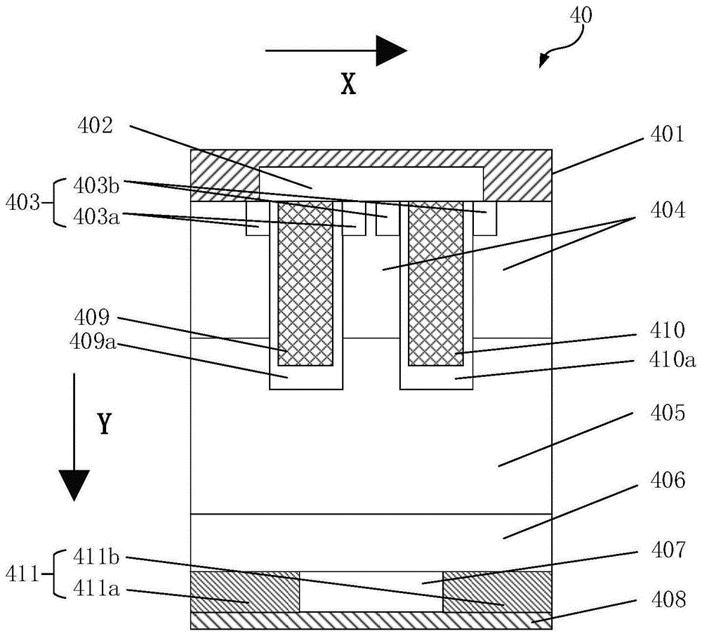
参阅图4,图4是本申请提供的半导体器件第一实施例的结构示意图,在本实施例中,该半导体器件为IEGT,其中,IEGT40包括层叠设置的第一金属层401、绝缘层402、N+型发射极区403、P型基区404、N型漂移区405、N型缓冲区406、P+型集电极区407以及第二金属层408。其中,第一金属层401设置于N+型发射极区403远离P+型集电极区407的一侧,第二金属层408设置于P+型集电极区407远离N+型发射极区403的一侧。Referring to FIG. 4, FIG. 4 is a schematic structural diagram of a first embodiment of a semiconductor device provided by the present application. In this embodiment, the semiconductor device is an IEGT, wherein the IEGT 40 includes a
可选地,IEGT40还包括第一栅极409和第二栅极410,其中,第一栅极409和第二栅极410为沟槽栅,设置于对应的沟槽内,并贯穿N+型发射极区403、P型基区404以及部分N型漂移区405;本实施例中,第一栅极409和第二栅极410可以与IEGT40的上表面垂直设置,在其他一些实施例中,第一栅极409和第二栅极410与IEGT40的上表面也可以设计一定的倾斜角度(例如20度),这样的方式可以减小载流子在沟槽处移动所承受到的散射阻力,进而降低IEGT40的导通压降。Optionally, the
可选地,N+型发射极区403包括第一N+型发射极区403a和第二N+型发射极区403b,其中,第一N+型发射极区403a和第二N+型发射极区403b沿横向方向间隔设置,该横向方向也即是图4中所示的X箭头所表示的方向,并且第一栅极409贯穿第一N+型发射极区403a,第二栅极410贯穿第二N+型发射极区403b,也即是第一N+型发射极区403a设置于第一栅极409的两侧,第二N+型发射极区403b设置于第二栅极410的两侧。Optionally, the N+-
可选地,第一栅极409和第二栅极410与对应的沟槽之间分别设置有第一栅极氧化层409a和第二栅极氧化层410a,其中,第一栅极氧化层409a和第二栅极氧化层410a分别覆盖每个沟槽的表面,且与栅极和P型基区404相接触;第一栅极409和第二栅极410则填充设置于栅极氧化层远离N型漂移区405的一侧,并且,第一栅极409和第二栅极410的深度小于对应沟槽的深度,深度方向也即是图4中所示的Y箭头表示的方向,其中,Y箭头表示的方向为第一栅极409和第二栅极410深度的延伸方向。Optionally, a first
进一步地,IEGT40还包括贯穿于P+型集电极区407的N+型集电极区411,其中,N+型集电极区411包括第一N+型集电极区411a和第二N+型集电极区411b,第一N+型集电极区411a和第二N+型集电极区411b在P+型集电极区407中沿横向方向间隔设置,且均与N型缓冲区406连接。在本实施例中,第一N+型集电极区411a和第二N+型集电极区411b可以分别设置于P+型集电极区407中沿横向方向的两端,且分别与第一栅极409和第二栅极410对应设置。Further, the
本实施例中,在给栅极施加正向电压时,形成第一栅极409和第二栅极410的区域发生反向而形成的电子沟道可连通N+型发射极区403和N型漂移区405,以实现整个IEGT40的开关功能。具体的,当加在栅极和源极两极的电压为正且大于开启电压时,会在IEGT40中的MOSFET内形成沟道并为半导体器件提供电流以使IEGT40导通;当在栅极和源极不加信号或加反向电压时,MOSFET内的沟道消失,IEGT内的电流被切断,IEGT40即关断。In this embodiment, when a forward voltage is applied to the gate, the electron channel formed by the reverse of the regions where the
可以理解的,绝缘层402可以在制作过程或使用过程中充分保护第一栅极409和第二栅极410,从而使该IEGT40的器件稳定性更好。其中,绝缘层402设置于第一栅极409与第一金属层401之间,以及第二栅极410和第二金属层401之间。并且,第一栅极409和第二栅极410横向方向上的宽度要大于一般的半导体器件结构的栅极宽度。It can be understood that the insulating
可选地,IEGT40还可以包括N+型阻止区(图未示),该N+型阻止区设置于N型漂移区405和N型缓冲区406之间,形成FS结构。Optionally, the
在一些实施例中,形成IEGT40的具体材料类型不受特别的限制,本领域常用的IGBT基材均可,本领域技术人员可根据半导体器件的具体电性能要求进行相应的选择。在一些实施例中,形成N+型发射极区403、P型基区404、N型漂移区405以及P+型集电极区407的材料可以为Si,因为硅基制成的半导体器件稳定性更佳、电压较低且适应性强。在另一些实施例中,形成上述基层的材料还可以为SiC,使得IEGT40的耐电压性能更好、电流更大且电压更高。In some embodiments, the specific type of material for forming the IEGT40 is not particularly limited, and any IGBT substrate commonly used in the art can be used, and those skilled in the art can make corresponding selections according to the specific electrical performance requirements of the semiconductor device. In some embodiments, the material for forming the N+-
在本实施例中,通过在IEGT40的背面P+型集电极区407中周期性的注入N+离子,从而在P+型集电极区407沿横向的两端,形成贯穿P+型集电极区407的第一N+型集电极区411a和第二N+型集电极区411b,使得P+型集电极区407附近的空穴载流子的移动通道变窄,从而限制了空穴的注入效率,而电子的注入效率进一步提升,本实施例中载流子的密度分布如图5所示,图5中虚线部分表示现有半导体器件中载流子的密度分布情况,实线部分则表示本实施例中载流子的密度分布情况,可以看出,相比于一般的IEGT,新颖的IEGT40结构降低了背部P+型集电极区407附近的载流子浓度,而增加了栅极附近以及发射极附近的载流子浓度,这样的结构有利于降低IEGT40栅极附近以及N型漂移区405的电阻,从而降低器件的导通压降与通态损耗。In this embodiment, by periodically injecting N+ ions into the P+-
可以理解的是,载流子浓度构成的变化,对于半导体器件的关断特性是有利的,当器件关断时,器件内部通常残留大量的空穴载流子,从而能够延长器件的关断时间。如果器件载流子浓度分布中,空穴浓度减少而电子浓度增加,就能够改善器件的关断时间与关断损耗。It can be understood that the change in the composition of the carrier concentration is beneficial to the turn-off characteristics of the semiconductor device. When the device is turned off, a large number of hole carriers usually remain inside the device, which can prolong the turn-off time of the device. . If the hole concentration decreases and the electron concentration increases in the carrier concentration distribution of the device, the turn-off time and turn-off loss of the device can be improved.
在其他的一些实施例中,N+型集电极区411可以贯穿P+型集电极区407以及至少部分的N型缓冲区406,这样的结构能够进一步限制空穴的注入效率,进而改善器件内部的载流子浓度平衡。其中,N+型集电极区411还可以贯穿所有N型缓冲区406,直接与N型漂移区405连接。In some other embodiments, the N+-type collector region 411 may penetrate through the P+-
因此在本实施例中,通过在IEGT40的背面P+型集电极区407中周期性的注入N+离子,从而形成N+型集电极区411与P+型集电极区407的周期性结构,从而降低器件内部空穴的注入效率,改善IEGT40内部载流子浓度的平衡。Therefore, in this embodiment, by periodically injecting N+ ions into the P+
参阅图6,图6是本申请提供的半导体器件第二实施例的结构示意图,在本实施例中,该半导体器件为IEGT,其中,IEGT60包括层叠设置的第一金属层601、绝缘层602、N+型发射极区603、P型基区604、N型漂移区605、N型缓冲区606、P+型集电极区607以及第二金属层608;以及上述实施例中贯穿N+型发射极区603、P型基区604以及部分N型漂移区605的第一栅极609和第二栅极610。其中,N+型发射极区603包括第一N+型发射极区603a和第二N+型发射极区603b,均沿着IEGT60的横向方向间隔设置,也即是图6中所示的X方向。Referring to FIG. 6, FIG. 6 is a schematic structural diagram of a second embodiment of a semiconductor device provided by the present application. In this embodiment, the semiconductor device is an IEGT, wherein the
IEGT60进一步包括设置于第一栅极609与对应沟槽之间的第一栅极氧化层609a,以及设置于第二栅极610与对应沟槽之间的第二栅极氧化层610a,其中,第一栅极609和第二栅极610填充设置于栅极氧化层远离N型漂移区605的一侧。The
进一步地,IEGT60还包括贯穿于P+型集电极区607的N+型集电极区611,与上一实施例的区别在于,本实施例中的N+型集电极区611的数量为多个,如图6所示,图6中三个N+型集电极区611可以将P+型集电极区607分割为两个,此时有两个N+型集电极区611则是设置于P+型集电极区607横向方向的两端;也可以将P+型集电极区607分割为三个或四个,此时N+型集电极区611则是设置于P+型集电极区607的中间部分,以使多个N+型集电极区611和多个P+型集电极区607横向交替设置。此处对数量不做具体限定。Further, the
在本实施例中,多个N+型集电极区611与多个P+型集电极区607组成的周期性结构,进一步限制了空穴的注入效率,而电子的注入效率进一步提升,有利于降低背部P+型集电极区607附近的载流子浓度,而增加第一栅极609、第二栅极610以及发射极金属电极附近的载流子浓度,进一步平衡IEGT60内部的载流子浓度。In this embodiment, the periodic structure composed of a plurality of N+
参阅图7,图7是本申请提供的半导体器件第三实施例的结构示意图,在本实施例中,该半导体器件为IEGT,其中,IEGT70包括层叠设置的第一金属层701、绝缘层702、N+型发射极区703、P型基区704、电子存储层705、N型漂移区706、N型缓冲区707、P+型集电极区708以及第二金属层709;还包括贯穿N+型发射极区703、P型基区704以及部分N型漂移区706的第一栅极710和第二栅极711。Referring to FIG. 7, FIG. 7 is a schematic structural diagram of a third embodiment of the semiconductor device provided by the present application. In this embodiment, the semiconductor device is an IEGT, wherein the
IEGT70进一步包括设置于第一栅极710与对应沟槽之间的第一栅极氧化层710a,以及设置于第二栅极711与对应沟槽之间的第二栅极氧化层711a,其中,第一栅极710和第二栅极711填充设置于栅极氧化层远离N型漂移区706的一侧。The
与前述实施例不同的是,本实施例在P型基区704和N型漂移区706之间设置有电子存储层705,该电子存储层705用于俘获空穴,并且,N+型发射极区703中的第一N+型发射极区703a和第二N+型发射极区703b分别设置于第一栅极710和第二栅极711相背的两侧,也即是第一栅极710和第二栅极711相互远离一侧。Different from the previous embodiment, this embodiment is provided with an
具体地,通过在IEGT70的P型基区704底部注入高浓度的N+离子,形成N+型电子存储层,该N+型电子存储层可以作为空穴的俘获陷阱,由于注入的N+离子带负电,而空穴带正电,因此,N+型电子存储层内的大量自由电子吸引N型漂移区706远离第一金属层701一侧方向上的空穴载流子向电子存储层705进行移动,以使得电子与空穴进行复合,同时该复合过程会增加电子存储层705附近区域电子和空穴的密度,也即是提高了电子存储层705附近区域的载流子密度,同时IEGT70中的N型缓冲区707附近区域由于流失了部分空穴,因此使得N型缓冲区707附近区域的载流子密度降低。Specifically, by injecting a high concentration of N+ ions at the bottom of the P-
进一步参阅图8,图8是本申请提供的半导体器件第三实施例中内部载流子密度的分布图,其中,虚线部分表示现有半导体器件中载流子的密度分布情况,实线部分则表示本实施例中载流子的密度分布情况,可以看出,由于电子存储层705的存在,使得栅极附近的载流子密度得到提升,同时集电极附近的载流子密度相对降低,这样的结构能够进一步平衡器件的载流子分布,以更适用于变频空调等家用电器的应用。Further referring to FIG. 8, FIG. 8 is a distribution diagram of the internal carrier density in the third embodiment of the semiconductor device provided by the present application, wherein the dotted line part represents the carrier density distribution in the existing semiconductor device, and the solid line part is Representing the carrier density distribution in this embodiment, it can be seen that due to the existence of the
因此在本实施例中,通过在P型基区704和N型漂移区706之间注入高浓度的N+离子形成N+型电子存储层的方式,使得电子存储层705附近区域的载流子密度增加,在增大栅极宽度初步平衡IEGT内部载流子浓度的基础上,进一步平衡了IEGT40内部的载流子浓度。Therefore, in this embodiment, the N+ type electron storage layer is formed by injecting a high concentration of N+ ions between the P-
参阅图9,图9是本申请提供的半导体器件第四实施例的结构示意图,在本实施例中,该半导体器件为RC-IEGT(ReverseConducting IEGT,逆导型IEGT),对于逆导型IEGT中的IEGT而言,通常希望发射机附近的电子电流越高越好,这样有利于改善栅极附近的调制电导,降低关断损耗;而对于逆导型IEGT中反并联的FRD(Fast recovery diode,快恢复二极管)而言,为了降低反向恢复峰值电流以及改善开关的软度,通常希望降低发射极附近的电荷浓度,这是RC-IGBT的固有矛盾。Referring to FIG. 9, FIG. 9 is a schematic structural diagram of a fourth embodiment of a semiconductor device provided by the present application. In this embodiment, the semiconductor device is an RC-IEGT (Reverse Conducting IEGT, reverse conducting IEGT). For the reverse conducting IEGT For the IEGT, it is usually hoped that the electron current near the transmitter is as high as possible, which is beneficial to improve the modulation conductance near the gate and reduce the turn-off loss; and for the anti-parallel FRD (Fast recovery diode) in the reverse conduction type IEGT, For fast recovery diodes), in order to reduce the peak reverse recovery current and improve the softness of the switch, it is usually desirable to reduce the charge concentration near the emitter, which is an inherent contradiction of RC-IGBTs.
因此,在本实施例中,RC-IEGT90包括层叠设置的第一金属层901、绝缘层902、N+型发射极区903、P型基区904、N型漂移区905、N型缓冲区906、P+型集电极区907以及第二金属层908。还包括贯穿N+型发射极区903、P型基区904以及部分N型漂移区905的第一栅极909和第二栅极910。Therefore, in this embodiment, the RC-
可选地,N+型发射极区903包括第一N+型发射极区903a和第二N+型发射极区903b,其中,第一N+型发射极区903a设置于第一栅极909靠近第二栅极910一侧,并与第一栅极氧化层909a和第一金属层901连接;第二N+型发射极区903b设置于第二栅极910靠近第一栅极909一侧,并与第二栅极氧化层910a和第一金属层901连接。与普通的半导体器件结构相比,去除了P型基区904上的栅极外侧的N+型发射极区903。Optionally, the N+
进一步地,RC-IEGT90还包括贯穿于P+型集电极区907的N+型集电极区911,其中,N+型集电极区911包括第一N+型集电极区911a和第二N+型集电极区911b,第一N+型集电极区911a和第二N+型集电极区911b在P+型集电极区907中沿横向方向间隔设置,在一些实施例中,N+型集电极区911还可以贯穿部分N型缓冲区906。在本实施例中,第一N+型集电极区911a与第二N+型集电极区911b分别设置于P+型集电极区907和N型缓冲区906沿横向方向的两端。Further, the RC-
在本实施例中,由于N+型发射极区903设置于第一栅极909和第二栅极910的内侧,两者的相对外侧也即是相互远离的一侧没有设置发射极;此时,在第一栅极909和第二栅极910相对外侧的深度方向(Y方向)上,半导体器件背面的P+型集电极区907和N型缓冲区906中掺入N+离子而形成的N+型集电极区911,与正面去除部分发射极区的P型基区904相对布局,形成了P-N的结构,也即是形成了FRD,这样使得集成的FRD与IEGT两者被集电极区的周期性结构在一定程度上相互隔离,使得两者在结构上相对独立的分割开来,相对独立的FRD和IEGT可以缓解半导体器件中发射极载流子密度要求的固有矛盾。In this embodiment, since the N+
在一些实施例中,第一栅极909和第二栅极910的深度不受特别的限制,本领域技术人员可以根据该半导体器件的具体电性能要求进行相应地设计。在一些实施例中,第一栅极909和第二栅极910的底部与P型基区904靠近N型漂移区905的上表面之间的间距可以为0.2至1微米,如此,栅极可以较好的控制电导调节效应。在一些具体实施例中,每个栅极的底部与P型基区904靠近N型漂移区905的上表面之间的间距可以为0.5微米。In some embodiments, the depths of the
在其他一些实施例中,第一栅极909和第二栅极910的深度可以大于半导体器件整体深度的1/3,且小于半导体器件整体深度的1/2,这样的结构设计可以进一步加强FRD与IEGT之间近似相对独立的布局,从而能够进一步地缓解两者对于发射极载流子密度需求不同的矛盾。In some other embodiments, the depth of the
在一些实施例中,第一栅极909和第二栅极910之间的间距不受特别的限制,本领域技术人员可以根据该半导体器件的具体电性能要求进行相应地设计。在一些实施例中,第一栅极909和第二栅极910之间的间距可以为1至3微米,如此,可以提半导体器件可流过的最大电流密度。在一些具体实施例中,第一栅极909和第二栅极910之间的间距可以为2微米。In some embodiments, the distance between the
参阅图10,图10是本申请提供的半导体器件的制作方法第一实施例的流程示意图,该方法包括:Referring to FIG. 10, FIG. 10 is a schematic flowchart of a first embodiment of a method for fabricating a semiconductor device provided by the present application. The method includes:
S11:提供一半导体衬底。S11: Provide a semiconductor substrate.
其中,半导体衬底的材料可以为氮化硅。The material of the semiconductor substrate may be silicon nitride.
S12:在半导体衬底上制作栅极。S12: forming a gate on the semiconductor substrate.
具体的,步骤S12主要包括:在半导体衬底上制作第一沟槽和第二沟槽,第一沟槽和第二沟槽贯穿N+型发射极区、P型基区和部分N型漂移区;分别在第一沟槽和第二沟槽中形成第一栅极和第二栅极。Specifically, step S12 mainly includes: forming a first trench and a second trench on the semiconductor substrate, and the first trench and the second trench pass through the N+ type emitter region, the P type base region and part of the N type drift region ; A first gate and a second gate are formed in the first trench and the second trench, respectively.
S13:分别制作P型基区和N+型发射极区。S13: respectively making a P-type base region and an N+-type emitter region.
其中,第一栅极、第二栅极、P型基区和N+型发射极区组成了半导体器件的有源区。The first gate, the second gate, the P-type base region and the N+-type emitter region constitute the active region of the semiconductor device.
S14:在P型基区远离N+型发射极区的一侧分别制作N型漂移区和N型缓冲区。S14: respectively forming an N-type drift region and an N-type buffer region on the side of the P-type base region away from the N+-type emitter region.
S15:在N型缓冲区远离N型漂移区的一侧制作P+型集电极区和N+型集电极区。S15: A P+-type collector region and an N+-type collector region are formed on the side of the N-type buffer zone away from the N-type drift region.
其中,N+型集电极区贯穿P+型集电极区,并与N型缓冲区连接。The N+-type collector region runs through the P+-type collector region and is connected to the N-type buffer region.
其中,N+型发射极区、P型基区、N型漂移区、N型缓冲区、集电极区为层叠设置,且都是通过离子注入的方式形成。The N+-type emitter region, P-type base region, N-type drift region, N-type buffer region, and collector region are stacked and formed by ion implantation.
参阅图11,图11是本申请提供的半导体器件的制作方法第二实施例的流程示意图,该方法包括:Referring to FIG. 11 , FIG. 11 is a schematic flowchart of a second embodiment of a method for fabricating a semiconductor device provided by the present application, and the method includes:
S201、场限环的注入、推阱:对硅片进行高温氧化,并在其表面生长出注入掩膜,通过光刻版进行离子注入,并进行高温推阱,再进行退火工艺,形成场限环结构,根据光刻窗口的不同,在退火后放入P型场限环。S201. Implantation and trap push of the field confinement ring: perform high temperature oxidation on the silicon wafer, grow an implantation mask on its surface, perform ion implantation through a lithography plate, and perform high temperature well push, and then perform an annealing process to form a field limit The ring structure, depending on the lithographic window, is placed in a P-type field-limiting ring after annealing.
S202、刻蚀有源区:在硅片表面生长一层厚度为0.3至0.5微米的场氧,光刻出有源区,有源区包括N+型发射极区、P型基区和栅极结构。S202. Etching the active area: grow a layer of field oxygen with a thickness of 0.3 to 0.5 microns on the surface of the silicon wafer, and photolithographically form the active area. The active area includes an N+ type emitter area, a P type base area and a gate structure .
S203、制作栅极:在硅片表面淀积一层TEOS保护层,光刻出窗口进行沟槽刻蚀,进而形成栅极结构的第一沟槽和第二沟槽,并在沟槽内壁形成栅氧化层,而后在沟槽内淀积多晶硅,分别形成第一栅极和第二栅极。S203, making the gate: depositing a TEOS protective layer on the surface of the silicon wafer, lithography out the window for trench etching, and then forming the first trench and the second trench of the gate structure, and forming the inner wall of the trench A gate oxide layer is formed, and then polysilicon is deposited in the trench to form a first gate electrode and a second gate electrode, respectively.
S204、P型基区与N+型发射极区的注入、推阱:通过离子注入P型杂质和N型杂质制作器件,并进行高温推阱,在退火后形成器件的P型基区和N+型发射极区。S204. Implantation and well push of P-type base region and N+-type emitter region: The device is fabricated by ion implantation of P-type impurity and N-type impurity, and high-temperature push-well is performed, and the P-type base region and N+-type of the device are formed after annealing. emitter region.
S205、发射极的制作:在器件表面淀积金属,采用光刻、刻蚀工艺,形成第一金属层,也即是发射极金属。S205 , making the emitter: depositing metal on the surface of the device, and using photolithography and etching processes to form a first metal layer, that is, the emitter metal.
S206、N+型阻止区的注入:通过离子注入N+型杂质,形成器件的电场阻止区。S206, implantation of N+ type blocking region: forming an electric field blocking region of the device by ion implanting N+ type impurities.
S207、N型缓冲区与P+型集电极区的注入:通过离子注入N+型杂质,在结晶质量高的硅片中形成缓冲区;翻转硅片,减薄硅片厚度,在硅片背面注入P型杂质并退火,形成P+型集电极区。S207. Implantation of N-type buffer and P+-type collector region: by ion implantation of N+-type impurities, a buffer zone is formed in the silicon wafer with high crystal quality; the silicon wafer is turned over, the thickness of the silicon wafer is reduced, and P is injected into the back of the silicon wafer type impurities and annealed to form a P+ type collector region.
S208、N+型集电极区的注入:在P+型集电极区中周期性注入N+型杂质并退火,形成N+型集电极区。其中,N+型集电极区和P+型集电极区横向交替设置。S208, implantation of N+ type collector region: periodically injecting N+ type impurities into the P+ type collector region and annealing to form an N+ type collector region. Wherein, the N+-type collector regions and the P+-type collector regions are arranged alternately laterally.
S209、背金退火:对硅片背面进行背面激光退火工艺。S209, back gold annealing: perform a backside laser annealing process on the backside of the silicon wafer.
S210、制作集电极:背面淀积金属形成第二金属层,也即是集电极。S210, making a collector electrode: depositing metal on the backside to form a second metal layer, that is, a collector electrode.
上述的制作方法,在原有IGBT产线上通过有限制程改进的生产工艺,可以缩短研制时间,降低生产成本。The above-mentioned manufacturing method can shorten the development time and reduce the production cost by adopting a limited-process improved production process on the original IGBT production line.
在本说明书的描述中,术语“连接”应作为广义理解,例如,“连接”可以是固定连接,也可以是可拆卸连接,或一体地连接;可以是直接相连,也可以通过中间媒介间接相连。对于本领域的普通技术人员而言,可以根据具体情况理解上述属于在本申请中的具体含义。In the description of this specification, the term "connection" should be understood in a broad sense. For example, "connection" can be a fixed connection, a detachable connection, or an integral connection; it can be directly connected or indirectly connected through an intermediate medium. . For those of ordinary skill in the art, the above-mentioned specific meanings in the present application can be understood according to specific situations.
在本说明书的描述中,术语“一个实施例”、“另一个实施例”等的描述意指结合该实施例或示例描述的具体特征、结构、材料或特点包含于本申请的至少一个实施例或示例中。在本说明书中,对上述术语的示意性表述不一定指的是相同的实施例或示例。而且,描述的具体特征、结构、材料或特点可以在任何的一个或多个实施例或示例中以合适的方式结合。In the description of this specification, the description of the terms "one embodiment", "another embodiment", etc. means that a particular feature, structure, material or characteristic described in connection with the embodiment or example is included in at least one embodiment of the present application or in the example. In this specification, schematic representations of the above terms do not necessarily refer to the same embodiment or example. Furthermore, the particular features, structures, materials or characteristics described may be combined in any suitable manner in any one or more embodiments or examples.
以上所述仅为本申请的实施方式,并非因此限制本申请的专利范围,凡是利用本申请说明书及附图内容所作的等效结构或等效流程变换,或直接或间接运用在其他相关的技术领域,均同理包括在本申请的专利保护范围内。The above description is only an embodiment of the present application, and is not intended to limit the scope of the patent of the present application. Any equivalent structure or equivalent process transformation made by using the contents of the description and drawings of the present application, or directly or indirectly applied to other related technologies Fields are similarly included within the scope of patent protection of this application.
Claims (14)
Priority Applications (1)
| Application Number | Priority Date | Filing Date | Title |
|---|---|---|---|
| CN202010839185.0A CN112018174A (en) | 2020-08-19 | 2020-08-19 | Semiconductor device, manufacturing method thereof and household appliance |
Applications Claiming Priority (1)
| Application Number | Priority Date | Filing Date | Title |
|---|---|---|---|
| CN202010839185.0A CN112018174A (en) | 2020-08-19 | 2020-08-19 | Semiconductor device, manufacturing method thereof and household appliance |
Publications (1)
| Publication Number | Publication Date |
|---|---|
| CN112018174A true CN112018174A (en) | 2020-12-01 |
Family
ID=73505175
Family Applications (1)
| Application Number | Title | Priority Date | Filing Date |
|---|---|---|---|
| CN202010839185.0A Pending CN112018174A (en) | 2020-08-19 | 2020-08-19 | Semiconductor device, manufacturing method thereof and household appliance |
Country Status (1)
| Country | Link |
|---|---|
| CN (1) | CN112018174A (en) |
Cited By (3)
| Publication number | Priority date | Publication date | Assignee | Title |
|---|---|---|---|---|
| CN115295613A (en) * | 2022-10-08 | 2022-11-04 | 烟台台芯电子科技有限公司 | A kind of fast recovery diode structure and its manufacturing method |
| CN115799255A (en) * | 2022-12-29 | 2023-03-14 | 上海鼎泰匠芯科技有限公司 | Semiconductor device and method for manufacturing the same |
| CN115810673A (en) * | 2022-12-21 | 2023-03-17 | 深圳市威兆半导体股份有限公司 | Diode device |
Citations (8)
| Publication number | Priority date | Publication date | Assignee | Title |
|---|---|---|---|---|
| US20090283799A1 (en) * | 2008-05-13 | 2009-11-19 | Infineon Technologies Ag | Reduced Free-Charge Carrier Lifetime Device |
| JP2010171057A (en) * | 2009-01-20 | 2010-08-05 | Denso Corp | Semiconductor device, and method of manufacturing the same |
| JP2015144220A (en) * | 2013-12-27 | 2015-08-06 | 良孝 菅原 | High performance semiconductor device and its operation method |
| CN105261564A (en) * | 2015-11-04 | 2016-01-20 | 株洲南车时代电气股份有限公司 | Preparation method for reverse-conducting IGBT |
| CN105990411A (en) * | 2014-09-11 | 2016-10-05 | 株式会社东芝 | Semiconductor device |
| CN108565284A (en) * | 2018-03-07 | 2018-09-21 | 嘉兴斯达半导体股份有限公司 | A kind of inverse conductivity type IGBT of trench gate field cut-off |
| CN109244125A (en) * | 2017-06-29 | 2019-01-18 | 万国半导体(开曼)股份有限公司 | Introduce the reverse conduction IGBT and preparation method thereof in epitaxial layer field stop area |
| CN111430453A (en) * | 2020-03-11 | 2020-07-17 | 上海擎茂微电子科技有限公司 | RC-IGBT chip with good reverse recovery characteristic and manufacturing method thereof |
-
2020
- 2020-08-19 CN CN202010839185.0A patent/CN112018174A/en active Pending
Patent Citations (8)
| Publication number | Priority date | Publication date | Assignee | Title |
|---|---|---|---|---|
| US20090283799A1 (en) * | 2008-05-13 | 2009-11-19 | Infineon Technologies Ag | Reduced Free-Charge Carrier Lifetime Device |
| JP2010171057A (en) * | 2009-01-20 | 2010-08-05 | Denso Corp | Semiconductor device, and method of manufacturing the same |
| JP2015144220A (en) * | 2013-12-27 | 2015-08-06 | 良孝 菅原 | High performance semiconductor device and its operation method |
| CN105990411A (en) * | 2014-09-11 | 2016-10-05 | 株式会社东芝 | Semiconductor device |
| CN105261564A (en) * | 2015-11-04 | 2016-01-20 | 株洲南车时代电气股份有限公司 | Preparation method for reverse-conducting IGBT |
| CN109244125A (en) * | 2017-06-29 | 2019-01-18 | 万国半导体(开曼)股份有限公司 | Introduce the reverse conduction IGBT and preparation method thereof in epitaxial layer field stop area |
| CN108565284A (en) * | 2018-03-07 | 2018-09-21 | 嘉兴斯达半导体股份有限公司 | A kind of inverse conductivity type IGBT of trench gate field cut-off |
| CN111430453A (en) * | 2020-03-11 | 2020-07-17 | 上海擎茂微电子科技有限公司 | RC-IGBT chip with good reverse recovery characteristic and manufacturing method thereof |
Cited By (3)
| Publication number | Priority date | Publication date | Assignee | Title |
|---|---|---|---|---|
| CN115295613A (en) * | 2022-10-08 | 2022-11-04 | 烟台台芯电子科技有限公司 | A kind of fast recovery diode structure and its manufacturing method |
| CN115810673A (en) * | 2022-12-21 | 2023-03-17 | 深圳市威兆半导体股份有限公司 | Diode device |
| CN115799255A (en) * | 2022-12-29 | 2023-03-14 | 上海鼎泰匠芯科技有限公司 | Semiconductor device and method for manufacturing the same |
Similar Documents
| Publication | Publication Date | Title |
|---|---|---|
| CN113690321B (en) | Silicon carbide trench gate MOSFET and manufacturing method thereof | |
| CN107275383B (en) | A Superjunction IGBT Containing Heterojunction | |
| CN108257953A (en) | The semiconductor devices of diode region not can be switched with IGBT areas and | |
| CN101308871A (en) | Insulated gate semiconductor device and manufacturing method thereof | |
| US9293559B2 (en) | Dual trench-gate IGBT structure | |
| CN102969350A (en) | Trench gate IGBT (Insulated Gate Bipolar Transistor) chip | |
| CN104299991A (en) | Semiconductor device | |
| CN108493242B (en) | A carrier-enhanced IGBT device with optimized internal electric field | |
| CN108447905A (en) | A kind of superjunction IGBT with trench isolations gate structure | |
| CN110518058A (en) | A kind of lateral trench type insulated gate bipolar transistor and preparation method thereof | |
| CN111834449A (en) | A fast turn-off RC-IGBT device with backside dual MOS structure | |
| CN112018174A (en) | Semiconductor device, manufacturing method thereof and household appliance | |
| CN105706241B (en) | MOS bipolar device | |
| CN108899363B (en) | Trench gate IGBT device capable of reducing on-voltage drop and turn-off loss | |
| WO2025026093A1 (en) | Igbt device and cellular structure thereof, and manufacturing method for cellular structure | |
| CN103956381B (en) | MOS grid-control thyristor | |
| CN110610986A (en) | An RC-IGBT Device Using Junction Termination Integrated Lateral Freewheeling Diode | |
| CN112018173A (en) | Semiconductor device, manufacturing method thereof and household appliance | |
| CN107134488A (en) | A kind of carrier stores enhanced insulated gate bipolar transistor | |
| CN208077982U (en) | insulated gate bipolar transistor | |
| JP7213398B2 (en) | insulated gate bipolar transistor | |
| CN113838915B (en) | Trench gate charge storage type IGBT and manufacturing method thereof | |
| CN110459596A (en) | A kind of lateral insulated gate bipolar transistor and preparation method thereof | |
| CN113471276B (en) | A dual-operating mode silicon carbide power device structure and manufacturing method thereof | |
| CN112331716B (en) | Semiconductor device, manufacturing method thereof and household appliance |
Legal Events
| Date | Code | Title | Description |
|---|---|---|---|
| PB01 | Publication | ||
| PB01 | Publication | ||
| SE01 | Entry into force of request for substantive examination | ||
| SE01 | Entry into force of request for substantive examination | ||
| RJ01 | Rejection of invention patent application after publication |
Application publication date: 20201201 |