CN1121016C - Method and system for configuring an array of logic devices - Google Patents
Method and system for configuring an array of logic devices Download PDFInfo
- Publication number
- CN1121016C CN1121016C CN97199308A CN97199308A CN1121016C CN 1121016 C CN1121016 C CN 1121016C CN 97199308 A CN97199308 A CN 97199308A CN 97199308 A CN97199308 A CN 97199308A CN 1121016 C CN1121016 C CN 1121016C
- Authority
- CN
- China
- Prior art keywords
- logic
- logical
- design
- logical block
- fpga
- Prior art date
- Legal status (The legal status is an assumption and is not a legal conclusion. Google has not performed a legal analysis and makes no representation as to the accuracy of the status listed.)
- Expired - Fee Related
Links
Images


Classifications
-
- G—PHYSICS
- G06—COMPUTING OR CALCULATING; COUNTING
- G06F—ELECTRIC DIGITAL DATA PROCESSING
- G06F30/00—Computer-aided design [CAD]
- G06F30/30—Circuit design
- G06F30/34—Circuit design for reconfigurable circuits, e.g. field programmable gate arrays [FPGA] or programmable logic devices [PLD]
Landscapes
- Engineering & Computer Science (AREA)
- Computer Hardware Design (AREA)
- Physics & Mathematics (AREA)
- Theoretical Computer Science (AREA)
- Evolutionary Computation (AREA)
- Geometry (AREA)
- General Engineering & Computer Science (AREA)
- General Physics & Mathematics (AREA)
- Design And Manufacture Of Integrated Circuits (AREA)
- Logic Circuits (AREA)
- Stored Programmes (AREA)
Abstract
Description
技术领域technical field
本发明总的涉及可编程逻辑器件,更具体地涉及现场可编程门阵列(FPGA)的配置。The present invention relates generally to programmable logic devices, and more particularly to the configuration of field programmable gate arrays (FPGAs).
背景技术Background technique
在集成电路技术的早期,诸如移位寄存器、多路转换器、加法器等的逻辑电路是由数字集成电路构成的。这些小规模集成(SSI)电路通常含有数目较少(例如四至八个)的逻辑门,如“与”门、“或”门、触发电路和锁存器等,需要几十个晶体管。随着技术的发展,能够将越来越多的晶体管装入到IC电路中。目前,半导体制造商能够将数百万个晶体管装在单个晶片上,从而形成高度复杂的芯片,如现代微处理器。In the early days of integrated circuit technology, logic circuits such as shift registers, multiplexers, adders, etc. were constructed from digital integrated circuits. These small-scale integration (SSI) circuits usually contain a small number (eg, four to eight) of logic gates, such as "AND" gates, "OR" gates, flip-flops, and latches, etc., requiring dozens of transistors. As technology develops, more and more transistors can be packed into IC circuits. Semiconductor manufacturers are currently able to pack millions of transistors on a single wafer, creating highly complex chips such as modern microprocessors.
装有这些VLSI(特大规模集成)和ULSI(超大规模集成)芯片的系统同样是复杂的。这种系统通常采用若干个常规逻辑芯片提供各种各样的支撑逻辑功能。已研制出允许制造商快速地实现客户的逻辑设计的门阵列。这些器件是由利用标准方法制造的逻辑门阵列组成的。器件的定制是在最后几步制造步骤中发生的,在这几步中形成与逻辑门连接的金属层以实现所需的逻辑功能。Systems incorporating these VLSI (Very Large Scale Integration) and ULSI (Ultra Large Scale Integration) chips are equally complex. Such systems typically employ several conventional logic chips to provide various supporting logic functions. Gate arrays have been developed that allow manufacturers to quickly implement customers' logic designs. These devices consist of arrays of logic gates fabricated using standard methods. Customization of the device occurs during the final few manufacturing steps, where the metal layers that interface with the logic gates are formed to achieve the desired logic function.
这些门阵列演变为可编程的器件,给仅需要少量器件或者还未完全开发逻辑设计但是需要少量样品作测试的设计人员提供了更大的灵活性。另一种可编程逻辑器件采用熔断器提供器件中逻辑门之间的互连。熔断器被熔断便断开连接,或者在所谓的抗熔断器的情况中形成连接。因此,这种器件只能使用一次,仅存储一组逻辑功能。The evolution of these gate arrays into programmable devices provides greater flexibility to designers who need only a few devices or who have not yet fully developed a logic design but need a small number of samples for testing. Another type of programmable logic device uses fuses to provide the interconnection between logic gates in the device. The fuse is blown to break the connection, or in the case of so-called anti-fuse fuses to make the connection. Therefore, the device can only be used once, storing only one set of logic functions.
可编程逻辑器件的继续发展已经导致可重新编程的互连关系的发展,更重要的是可配置的逻辑单元的发展。顾名思义,可配置逻辑单元允许设计人员能够对逻辑单元进行编程,使其具有许多基本逻辑门中任何一个门的功能或者更高级的逻辑功能。当前的制造技术使得生产具有数以千计个可配置逻辑单元及其相关互连的高密度器件,即称为现场可编程门阵列(FPGA)成为可能。提供这种高密度器件的能力使得设计人员能够采用越来越复杂的逻辑功能。象以前的产品一样,FPGA包括可编程的互连关系。此外,互连关系是可重复编程的,进一步增大了FPGA的利用价值。Continued development of programmable logic devices has led to the development of reprogrammable interconnects and, more importantly, configurable logic cells. As the name implies, configurable logic cells allow designers to program logic cells to function as any of a number of basic logic gates or to more advanced logic functions. Current manufacturing techniques make it possible to produce high-density devices with thousands of configurable logic cells and their associated interconnections, known as field-programmable gate arrays (FPGAs). The ability to provide such high-density devices enables designers to employ increasingly complex logic functions. Like previous products, FPGAs include programmable interconnects. In addition, the interconnection relationship is reprogrammable, which further increases the utilization value of FPGA.
然而,以往对这些可重复编程FPGA的重新配置通常需要对整个器件进行重新配置。Atmel公司(本发明的受让人)制造的FPGA代表了这种器件向前又迈进了一步。将这种器件称为可动态重新配置的FPGA,允许仅对所选的一部分逻辑阵列进行重新配置。用这种方法能够对FPGA作出变化,不必对整个器件进行编程,从而允许仅对所选的一部分阵列进行重新配置。However, historical reconfiguration of these reprogrammable FPGAs typically required reconfiguration of the entire device. FPGAs manufactured by Atmel Corporation (assignee of the present invention) represent another step forward for such devices. Such a device is called a dynamically reconfigurable FPGA, allowing only a selected portion of the logic array to be reconfigured. This approach enables changes to be made to the FPGA without programming the entire device, allowing reconfiguration of only selected portions of the array.
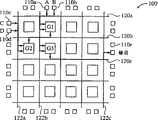
参考图1,典型的FPGA 100包括多个可配置的逻辑单元130、可配置的I/O块110和可配置的互连关系120、122,共同称之为FPGA资源。尽管互连关系120、122是以各个互连线网格示出的,但是每条“线”实际上是一组互连线,例如,如图3B所示。每个逻辑单元130和I/O块110包括数据线140、142,它们能够有选择地耦合到互连关系120、122上。Referring to FIG. 1, a
典型设计周期从设计一个或多个然后将在FPGA中实现的逻辑电路开始。逻辑设计包括逻辑门和这些逻辑门之间的互连关系。然而,特定的设计,如数字滤波器利用“常数”,即1和0的串来限定其特性。为了描述本发明,把这种常数称为设计的一部分,也可以称为逻辑门。A typical design cycle begins with designing one or more logic circuits that will then be implemented in an FPGA. A logic design consists of logic gates and the interconnection relationships between those logic gates. However, certain designs, such as digital filters, use "constants," strings of 1s and 0s, to define their characteristics. For purposes of describing the present invention, such constants are referred to as part of the design, and may also be referred to as logic gates.
例如,图2示出一种简单的逻辑设计。逻辑设计中的每个元件用一个实例名来识别。因此,图2中的与门和或门取名为G1-G3。图3A示出逻辑设计是如何在FPGA 100’中出现的。将图2中所示的门G1-G3中的每一个门和互连关系映射到图3A中所示的所选逻辑单元和互连关系上。同样,将输入A-D和输出OUT(图2)映射到所选I/O块。因此,互连关系120a-120c和122a-122c(以较淡的线表示)与逻辑单元G1-G3和I/O块110a-110e连接在一起。图3B示出了图3A配置中一部分放大图。说明不同逻辑单元、互连关系和I/O块之间的具体互连情况。尽管在该图中的设计并未示出常数的使用,但是,众所周知,能够将现代FPGA中逻辑单元构造为输出逻辑“1”或逻辑“0”,能够根据需要如此构造一组逻辑单元,产生一个或多个1和0的串。For example, Figure 2 shows a simple logic design. Each component in the logic design is identified by an instance name. Therefore, the AND gates and OR gates in Figure 2 are named G1-G3. Figure 3A shows how a logic design appears in FPGA 100'. Each of the gates G1-G3 shown in FIG. 2 and the interconnection are mapped onto the selected logic cells and interconnection shown in FIG. 3A. Likewise, map inputs A-D and outputs OUT (Figure 2) to the selected I/O block. Thus,
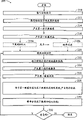
现在将说明把图2的设计转换到如图3A中所示的FPGA的步骤。由于绝大多数的目前设计在功能上趋向于相当复杂,通常采用计算机辅助设计(CAD)工具以便于设计过程。因此,在图4中,设计流程图200从输入逻辑电路初始设计,即步骤210开始,例如通过利用CAD工具。The steps for converting the design of Figure 2 to an FPGA as shown in Figure 3A will now be described. Since most current designs tend to be quite complex in function, computer aided design (CAD) tools are often employed to facilitate the design process. Thus, in FIG. 4, the design flow diagram 200 begins by entering an initial logic circuit design,
接着是逻辑电路的逻辑门的放置和选路,步骤212。作为放置和选路步骤的结果,产生设计数据库,步骤214。设计数据库规定FPGA中将参与实现逻辑电路的这些逻辑单元、I/O块和互连关系(即资源),包括所选资源的位置及其路经或逻辑结构。图1示出用于识别逻辑单元位置的若干坐标系中的一个。在图1所示的传统坐标系中,逻辑单元按照从左到右和从下到上的次序编号,从左下角单元(0,0)开始,到右上角单元(3,3)结束。通常,设计数据库另外还包括在设计阶段期间给逻辑电路元件指定的实例名,图2。Next is the placement and routing of the logic gates of the logic circuit,
从包含在设计数据库中的信息,由通常称为位流编译器的工具产生配置位流,步骤216。位流编译器获取存储在设计数据库中的位置和配置信息,产生将配置FPGA中各种资源的限定位流。在物理级上,限定位流代表FPGA中晶体管(开关)的开/关(ON/OFF)状态,它实际上控制每个逻辑单元和I/O块的配置以及逻辑单元与I/O块之间的互连。From the information contained in the design database, a configuration bitstream is generated,
在这里,或是可以把配置位流下载到逻辑阵列,由此而配置器件,步骤218a,或是可以把位流保存在磁盘上,步骤218b。图4中用虚线表示这两种可供选择的方案。Here, the configuration bitstream can either be downloaded to the logic array, thereby configuring the device,
即使已经对设计作了调试并按照预期的进行操作,偶然也会发生需要对初始设计进行变化。例如,新的要求可能导致功能定义的变化,这就必须改变初始设计。利用通常的现有技术,对初始设计的最终版本的修改,步骤220导致上述步骤的重复。因此,设计人员利用CAD工具访问初始设计的最终版本并对该设计作出所需改变。执行第二次放置和选路步骤,步骤222,由此产生第二个设计数据库,步骤224。然后,根据新的设计数据库由位流编译器产生第二个配置位流,步骤226。Even when a design has been debugged and is operating as expected, occasionally there will be a need to make changes to the original design. For example, new requirements may lead to changes in the functional definition, necessitating changes to the initial design. Modifications to the final version of the initial design,
与第一配置位流一样,可以把也可以不把第二配置位流下载到FPGA。如果需要下载,可提供两种选择:即能够把位流整体下载到FPGA,由此重新配置整个阵列,以包含改进的设计。另一种选择,这里FPGA是可动态重新配置的,意思是指器件能够被部分重新配置,能够仅对第二配置位流中对应于设计变化的这些部分进行下载。通过确定第一与第二配置位流之间的差异产生部分(可重新配置的)位流首先实现之,步骤228。然后,把部分位流下载到可动态重新配置的FPGA,步骤230,由此而实行FPGA的部分重新配置,其中,仅对改进设计中所涉及的这些逻辑单元、互连关系和I/O块进行重新编程。最后,对于另外的设计改进重复循环,就象出现设计功能要求上变化一样。Like the first configuration bitstream, the second configuration bitstream may or may not be downloaded to the FPGA. If downloading is required, two options are available: the ability to download the bitstream in its entirety to the FPGA, thereby reconfiguring the entire array to include the improved design. Another option, where the FPGA is dynamically reconfigurable, means that the device can be partially reconfigured, and only those parts of the second configuration bitstream corresponding to design changes can be downloaded. This is first achieved by determining the difference between the first and second configuration bitstreams,
设计中逻辑门的放置和选路是一项计算强度高的活动。当设计人员由于高密度FPGA的提供能力趋于采用越来越复杂的设计,放置和选路操作会大大增加。在图4所示的现有方法中,考虑到设计循环中的每一次迭代可能需要完全的放置和选路操作,专用于放置和选路计算的时间量会达到惊人的程度。The placement and routing of logic gates in a design is a computationally intensive activity. As designers tend to adopt increasingly complex designs due to the capabilities offered by high-density FPGAs, the placement and routing operations increase dramatically. In the existing approach shown in Figure 4, the amount of time dedicated to placement and routing computations can be astonishing, considering that each iteration in the design cycle may require a full placement and routing operation.
现有技术方法的另一个方面是可能会出现改进后的设计将导致放置和选路配置不同于以前设计的放置和选路配置。如果以前的设计已经精心地调谐到提供特定临界时序特性,这就成为一个问题。通过全部放置和选路操作进行的下一设计会导致具有不同净长度的逻辑的不同放置,由此对电路的时序产生不利影响。在涉及实时应用的地方,这是一种不可以接受的情况。Another aspect of the prior art approach is that it may occur that an improved design will result in a different placement and routing configuration than previously designed. This becomes a problem if the previous design has been carefully tuned to provide certain critical timing characteristics. The next design through all the placement and routing operations can result in different placements of logic with different net lengths, thereby adversely affecting the timing of the circuit. This is an unacceptable situation where real-time applications are involved.
需要一种对于完全完成和调试逻辑设计的重新设计在周转时间方面能改善现有技术的方法。还需要一种开发方法,维持现有设计中未涉及设计修改的部分不受影响。What is needed is an approach that improves upon the prior art in terms of turnaround time for redesign of fully completed and debugged logic designs. There is also a need for a development methodology that maintains unaffected portions of the existing design that did not involve design modifications.
到这里,讨论一直集中围绕逻辑电路的设计是在设计人员的工作实验室的环境中。然而,已观察到,FPGA的现场应用会不适合于单个静态设计。尽管FPGA可以在实际工作条件下在现场重新配置,但是,新的配置通常由存储在诸如EPROM的非易失性装置中的完整设计组成。从EPROM读出配置位流并将其下载到FPGA中。因此,可供使用的配置的尺寸受EPROM的存储容量的限制。在诸如自适应滤波的应用中,迫切需要滤波器的响应能够根据诸如被滤波数据的频率和相位特性,即通常不可预料的条件,在运行时变化。在这种情况中,事前便不能指定新的配置,如滤波器参数。Up to this point, the discussion has centered around the design of logic circuits in a designer's working laboratory environment. However, it has been observed that field applications of FPGAs may not be suitable for a single static design. Although FPGAs can be reconfigured in the field under actual operating conditions, the new configuration usually consists of the complete design stored in a non-volatile device such as an EPROM. Read the configuration bit stream from the EPROM and download it to the FPGA. Therefore, the size of the available configurations is limited by the storage capacity of the EPROM. In applications such as adaptive filtering, there is a strong need for the response of the filter to be able to vary at run-time based on conditions such as the frequency and phase characteristics of the data being filtered, i.e., often unpredictable conditions. In this case, new configurations such as filter parameters cannot be specified in advance.
然而,还需要在运行过程中根据装置正在工作的环境对FPGA进行配置的能力。此外,由于仅需要对FPGA中一部分进行重新配置,如在自适应滤波器的情况中,需要具有运行过程中进行部分重新配置的能力。However, there is also a need for the ability to configure the FPGA on the fly according to the environment in which the device is operating. Furthermore, since only a portion of the FPGA needs to be reconfigured, as in the case of adaptive filters, the ability to perform partial reconfiguration during operation is required.
发明概要Summary of the invention
根据本发明,一种对可动态重新配置FPGA进行配置的方法,从输入初始逻辑设计开始。在该设计上进行放置和选路,导致将位置分配给实现该设计的FPGA中的逻辑单元和互连关系。设计数据库是放置和选路操作的结果。接着,在设计数据库上工作的位流编译器产生配置位流。位流或是可以被下载到FPGA,由此对装置进行配置,或是可以简单地被保存在存储媒介上。According to the present invention, a method of configuring a dynamically reconfigurable FPGA begins with entering an initial logic design. Placement and routing are performed on the design, resulting in the assignment of locations to logic cells and interconnections in the FPGA implementing the design. The design database is the result of placement and routing operations. Next, a bitstream compiler operating on the design database generates a configuration bitstream. The bitstream can either be downloaded to the FPGA, thereby configuring the device, or it can simply be saved on a storage medium.
根据相应的设计数据库作出对初始设计最后工作版本的变化。修改后的设计数据库被保存起来,从修改后的设计数据库产生第二配置位流。根据本发明,第二配置位流仅由对应于修改后逻辑设计的这些逻辑单元、I/O块和互连关系的定义位串组成。Changes to the final working version of the initial design are made against the corresponding design database. A modified design database is saved, and a second configuration bitstream is generated from the modified design database. According to the present invention, the second configuration bit stream consists only of defined bit strings corresponding to these logic cells, I/O blocks and interconnection relations of the modified logic design.
通过直接访问设计数据库以执行设计的变化,完全可避免本来需要的耗费在放置和选路计算上的时间。当必须对逻辑设计的最后工作版本作修改时,例如,由于在装入FPGA的系统的功能要求上的变化需要修改时,这是尤其有用的,也是想要的特性。经常的情况是,设计变化自然越来越多,仅涉及到整个设计的一个局部部分。在其它时间,设计人员希望对逻辑设计的最后工作版本的变化做实验。本发明的配置方法可保证用很短的检修时间来实现设计变化,所以,渐增的变化和“What-if”实验是可行的和便利的,不会对项目开发产生不利影响也不产生停止工作时间表。此外,由于放置和选路操作是旁通的,设计中设计人员未作修改的关键部分的任何时序将不受影响并保证提供已知的时序性能。更通俗地说,设计中未作修改的任何部分将继续按预期行使其特性。因此,采用本发明的方法,保证产生的FPGA应用在结构上是正确的,因此功能上是正确的。By directly accessing the design database to perform design changes, time spent on placement and routing calculations that would otherwise be required is completely avoided. This is especially useful, and a desirable feature, when changes must be made to the last working version of the logic design, eg, due to changes in the functional requirements of the system incorporating the FPGA. It is often the case that design variations naturally multiply and involve only a partial portion of the overall design. At other times, the designer wishes to experiment with changes to the last working version of the logic design. The configuration method of the present invention ensures that design changes are implemented with very short turnaround times, so that incremental changes and "what-if" experiments are feasible and convenient without adversely affecting or stopping project development work schedule. Also, because the placement and routing operations are bypassed, any timing in critical portions of the design that are not modified by the designer will be unaffected and guaranteed to provide known timing performance. More generally, any part of the design that has not been modified will continue to function as intended. Therefore, using the method of the present invention, it is guaranteed that the generated FPGA application is correct in structure and therefore correct in function.
在本发明的一个较佳实施例中,通过图形接口把设计数据库提供给用户。接口允许用户指定一部分设计数据库进行显示。设计数据库通过其实例名和在FPGA中的位置确定逻辑单元、I/O块和互连关系。给用户提供逻辑单元,包括被配置为输出常数逻辑值的这些逻辑单元的名称、位置和当前配置。也给出逻辑单元当中的互连关系。In a preferred embodiment of the invention, the design database is presented to the user through a graphical interface. The interface allows the user to specify a portion of the design database for display. The design database identifies logic units, I/O blocks, and interconnection relationships through its instance names and locations in the FPGA. Logical cells are provided to the user, including the name, location, and current configuration of those logical cells configured to output constant logical values. The interconnection relationships among the logical units are also given.
通过从一张以图形方式或者文本方式表示的逻辑门和互连线选项的表或菜单中进行选择可以作出对设计数据库的修改。对于常数的修改可以以文本方式通过输入新的常数值或者以图形方式通过操纵一个或多个能够打开(逻辑“0”)或关闭(逻辑“1”)的开关的图标进行。Modifications to the design database may be made by selecting from a list or menu of graphically or textually represented logic gate and interconnect options. Modifications to constants can be made textually by entering new constant values or graphically by manipulating one or more icons that can be turned on (logic "0") or off (logic "1").
在本发明的另一个实施例中,对FPGA进行实时重新配置的系统包括与装置的硬件接口和为了下载新配置数据而访问该装置的软件实用程序。软件实用程序包括产生部分配置位流的手段,允许应用程序根据运行中检测到的操作环境中的特定条件对FPGA进行配置。硬件接口和软件实用程序允许在装置使用中访问FPGA,从而能够对装置中的一部分进行重新配置。In another embodiment of the invention, a system for real-time reconfiguration of an FPGA includes a hardware interface to the device and a software utility that accesses the device for downloading new configuration data. The software utility includes the means to generate a partial configuration bitstream that allows the application to configure the FPGA based on specific conditions detected in the operating environment on the fly. A hardware interface and software utility allow access to the FPGA while the device is in use, enabling reconfiguration of parts of the device.
附图简述Brief description of the drawings
图1是典型FPGA的结构。Figure 1 is the structure of a typical FPGA.
图2是逻辑电路的一个例子。Figure 2 is an example of a logic circuit.
图3A和3B示出图2的逻辑电路在图1的FPGA中的实施。3A and 3B illustrate the implementation of the logic circuit of FIG. 2 in the FPGA of FIG. 1 .
图4是在FPGA设计中通用步骤的要点。Figure 4 is a summary of common steps in FPGA design.
图5是本发明设计方法的一个实施例的要点。Figure 5 is a summary of one embodiment of the design method of the present invention.
图6是按本发明配置FPGA的系统的方框图。Figure 6 is a block diagram of a system for configuring an FPGA in accordance with the present invention.
图7A-7C示出数字滤波器设计。7A-7C illustrate digital filter designs.
图8A和8B是本发明的用户接口的屏幕样板。8A and 8B are screen templates of the user interface of the present invention.
图9A-9D示出利用基于ROM查找表实现的加法器电路和减法器电路。9A-9D illustrate adder circuits and subtractor circuits implemented using ROM-based look-up tables.
图10A-10B示出本发明的用户接口的屏幕样板。10A-10B illustrate screen templates of the user interface of the present invention.
图11示出一个实时FPGA重新配置的系统。Figure 11 shows a real-time FPGA reconfiguration system.
实现本发明的最佳方式BEST MODE FOR CARRYING OUT THE INVENTION
参考图5,按照本发明一个实施例的配置方法300包括创建一种初始设计,步骤310,和执行放置位置和选路径的操作,获得一个第一设计数据库,步骤312和314。然后,位流编译器创建配置位流,步骤316,可以将其下载到FPGA上,配置装置,步骤318a。另一方面,配置位流可以简单存储在存储器装置中,步骤318b。配置位流包括多个定义位流,它指定FPGA中的资源将如何进行配置。Referring to FIG. 5 , a configuration method 300 according to an embodiment of the present invention includes creating an initial design, step 310 , and performing placement and routing operations to obtain a first design database, steps 312 and 314 . The bitstream compiler then creates a configuration bitstream, step 316, which can be downloaded to the FPGA, configuring the device, step 318a. Alternatively, the configuration bitstream may simply be stored in the memory device, step 318b. The configuration bitstream consists of multiple definition bitstreams that specify how resources in the FPGA are to be configured.
当需要对初始逻辑设计的最终工作版本进行变化时,设计修改可以直接对设计数据库进行。然后,继续图5所示的方法300,向设计人员显示设计数据库中的一部分,步骤320。设计人员选择设计数据库中需要作修改的这些部分和输入变化,步骤322。根据输入的修改情况,产生部分配置位流(也称为重新配置位流),它仅由对应于修改的定义位流构成。然后,可以将这部分位流下载或保存到存储媒体中,步骤326。When changes are required to the final working version of the initial logical design, design modifications can be made directly to the design database. Then, continuing the method 300 shown in FIG. 5 , a portion of the design database is displayed to the designer, step 320 . The designer selects those parts of the design database to be modified and enters the changes, step 322 . Depending on the modification of the input, a partial configuration bitstream (also referred to as a reconfiguration bitstream) is generated, consisting only of the definition bitstream corresponding to the modification. This portion of the bitstream may then be downloaded or saved to a storage medium, step 326 .
图6示出对动态可配置FPGA进行配置的系统,它体现了图5所示的方法。系统400包括数据存储器420和各个模块402-420。采用诸如CAD工具、简图捕获程序等设计输入模块402来创建初始设计420a并存储到磁盘420上。放置和选路模块404获取初始设计420a并创建设计数据库420b,它也存储在磁盘上。位流编译器406产生配置位流420c,下载模块408把配置位流下载到FPGA150。FIG. 6 shows a system for configuring a dynamically configurable FPGA, which embodies the method shown in FIG. 5 .
设计人员通过图形用户接口(GUI)模块410输入对初始逻辑设计最终工作版本的修改。GUI从设计数据库420b进行读出并显示由设计人员所选的设计数据库中的一部分。GUI接收对设计数据库的修改并仅根据输入的修改创建部分位流。GUI装入位流编译器的功能,产生部分位流。然后将部分位流420d存储到磁盘上,接着通过下载模块408下载到FPGA。另一方面,GUI能够把部分位流直接传送到下载模块408。在这里应当注意:如果不需要间接下载到FPGA,那么能够采用另一种存储媒体来存储配置(和重新配置)位流。例如,可以把配置(和重新配置)位流下载到EEPROM等存储媒体上,以供下一步分配。The designer enters modifications to the final working version of the initial logic design through a graphical user interface (GUI)
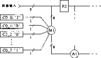
为了说明图6所示的方法,考虑一个自适应数字滤波器,如图7A中所示。滤波器设计500由串联级联的延迟寄存器R1-R7、乘法器M1-M8和加法器A1-A7组成。数据宽带为八位(一字节)。一组滤波器系数C0-C7起乘法运算的被乘数的作用。由于数据中的每个字节通过寄存器移位和传播,所有乘法器形成系数与数据之间的乘积项。然后由加法器A1-A7对乘积项求和。To illustrate the method shown in Figure 6, consider an adaptive digital filter, as shown in Figure 7A.
回想一下逻辑设计,如滤波器设计500中的每个元件具有一个由设计人员开始指定的实例名。因此,参考图7A,寄存器取名为R1-R7,乘法器取名为M1-M8,加法器取名为A1-A7。还给系数C0-C7指定了实例名。具体说,包含系数的每一个位具有一个名称。从图7C中所示的系数C0的扩展图中更加清楚地示出了这一情况。系数是一个八位量,这里,将位取名为C0_0至C0_7。再回到图7A,应当明白,也可以给元件R1-R7、M1-M8和A1-A7当中的互连关系取名。然而,为了避免图面的杂乱,已经省略了这些互连关系的实例名。Recalling logic design, each element in
滤波器设计500的放置和选路导致设计数据库,由实例名、每个寄存器和算术算符以及被选作实现这些功能的逻辑单元的位置和配置指定。以同样的方式,设计数据库列出位的实例名,包括系数C0-C7、它们的相应逻辑单元的位置和逻辑单元是否被配置为产生逻辑“0”或逻辑“1”。通过FPGA中的坐标系,如图1中所示的坐标系识别出现在设计数据库中的逻辑单元。Placement and routing of the
图7B示出图7A的数字滤波器的改进设计500’,这里已经指定了一组不同的系数C’0-C’7。希望根据本发明的方法作这种修改的设计人员开始访问基于初始设计500创建的第一设计数据库。这最好是利用图形用户接口(GUI)实现,当然基于文本的接口也一样是有效的,也许使用更困难和更低效些。FIG. 7B shows an improved design 500' of the digital filter of FIG. 7A, where a different set of coefficients C' 0 -C' 7 has been assigned. A designer wishing to make such modifications according to the method of the present invention begins by accessing a first design database created based on the
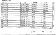
在一个实施例中,GUI有一种模式,用于对逻辑设计中所定义的逻辑常数进行编辑。例如,图8A的屏幕样板显示了设计500中的每个常数C0-C7。在“实例名”列下是包括每个系数C0-C7位的名称。每个位由一个配置为输出常数逻辑电平的逻辑单元实现。回想一下,每个逻辑单元具有一个相应的实例名。在单元被范围识别的地方,如在图8A的情况中,显示范围中第一和最后单元的实例名。在“位置”列下是在相应逻辑单元的FPGA中的位置。为了说明起见假设,被使用的坐标编号惯例遵循图1中所示的惯例。因此,根据图8A,包括系数C0的逻辑单元位于FPGA中第10行的第7-14列中;系数C1的逻辑单元位于第12行的第7-14列中,依此类推。“现行配置”列显示由逻辑单元产生的当前逻辑值。例如,包括系数C0的第7、8、9、10、11、12、13和14列中八个逻辑单元显示,为当前配置相应的输出逻辑值“1”、“0”、“1”、“0”、“1”、“0”、“1”和“1”。“新配置”列由输入字段组成,允许用户输入新的逻辑值,作为一位串。这位串位中的每个位与这位串所表示的常数单元具有一一对应关系。In one embodiment, the GUI has a mode for editing logic constants defined in the logic design. For example, the screen template of FIG. 8A shows each of the constants C 0 -C 7 in
由于设计数据库包含产生图8A所示显示屏所需的所有信息,GUI通过设计数据库进行简单搜索,找出已经被配置为产生常数逻辑电平的这些逻辑单元,访问它们的实例名、单元位置和当前配置信息。访问设计数据库和产生如图8A中所示显示信息的具体软件实施细节将随任何给定设计数据库格式所使用的精确数据结构而变化。在计算机程序员的范围和能力之内,这些实施细节是专业人员所公知的。Since the design database contains all the information needed to produce the display shown in Figure 8A, the GUI performs a simple search through the design database to find those logic cells that have been configured to generate constant logic levels, accessing their instance names, cell locations and Current configuration information. The specific software implementation details for accessing the design database and generating the display information as shown in Figure 8A will vary with the precise data structures used for any given design database format. These implementation details are well known to those skilled in the art, within the purview and ability of a computer programmer.
图8A中所示的逻辑常数最好按照水平相邻性分组。在一个给定的常数逻辑单元块中,可以将逻辑单元分组为水平单元组或垂直单元组。例如,在图8A中,可以看出,单元位置(7,18)至(14,21)限定32个逻辑单元的块。这些单元被显示为四个由八个水平相邻单元组成的组。因此,四个水平组是:(7,18)至(14,18);(7,19)至(14,19);(7,20)至(14,20)和(7,21)至(14,21)。The logical constants shown in Figure 8A are preferably grouped by horizontal contiguity. Within a given block of constant logical cells, logical cells can be grouped into horizontal cell groups or vertical cell groups. For example, in FIG. 8A, it can be seen that cell locations (7,18) through (14,21) define a block of 32 logical cells. The cells are shown as four groups of eight horizontally adjacent cells. Thus, the four level groups are: (7,18) to (14,18); (7,19) to (14,19); (7,20) to (14,20) and (7,21) to (14, 21).
另一方面,块(7,18)至(14,21)中的单元最好能够按照垂直相邻性分组。在图8B的屏幕样板中示出这一情况。在这种情况下,有八个由四个单元组成的垂直组,每一个为:(7,18)至(7,21);(8,18)至(8,21);(9,18)至(9,21);(10,18)至(10,21);(11,18)至(11,21);(12,18)至(12,21);(13,18)至(13,21)和(14,18)至(14,21)。于是将这些单元的其它字段修改反映其垂直分组。On the other hand, cells in blocks (7,18) to (14,21) can preferably be grouped by vertical adjacency. This is shown in the screen template of Figure 8B. In this case, there are eight vertical groups of four cells, each of: (7,18) to (7,21); (8,18) to (8,21); (9,18 ) to (9, 21); (10, 18) to (10, 21); (11, 18) to (11, 21); (12, 18) to (12, 21); (13, 18) to (13,21) and (14,18) to (14,21). The other fields of these cells are then modified to reflect their vertical grouping.
根据较佳实施例,将相邻常数单元的组表示为单元的范围。由于构成系数C0-C3的单元仅呈现水平相邻性它们显示成水平组。同样,对仅显示垂直相邻性的单元进行垂直分组。能够对常数单元进行垂直或水平分组的地方,按照用户指定的优先选择进行分组。因此,根据设计人员的优先选择,能够对系数C4-C7进行水平或垂直分组,如图8A和8B所示。在图中所示的例子中,优先选择可以针对水平相邻性,如图gA所示。然而,在另一种设计中,可以按垂直方式排列系数,在这种情况中,可以作出图8B所示的垂直优选。According to a preferred embodiment, groups of adjacent constant cells are represented as ranges of cells. Since the cells making up the coefficients C 0 -C 3 exhibit only horizontal adjacency they are shown in horizontal groups. Likewise, vertically group cells that only show vertical adjacency. Where constant cells can be grouped vertically or horizontally, grouping is done according to a user-specified preference. Thus, depending on the designer's preference, the coefficients C4 - C7 can be grouped horizontally or vertically, as shown in Figures 8A and 8B. In the example shown in the figure, the preference may be for horizontal adjacency, as shown in figure gA. However, in another design, the coefficients could be arranged in a vertical fashion, in which case the vertical preference shown in Figure 8B could be made.
在本发明的另一个实施例中,可以将非相邻的常数单元分组在一起。GUI允许用户选择常数单元中的任意组合并将所选单元作为一个组处理。尽管这些单元是非相邻的,但是,GUI可显示作为一个组的单元,并允许用户对作为一个组的单元的逻辑值进行修改。因此,以一一对应关系把由用户输入的代表新逻辑值的一位值串映射到组中的常数单元,与以上结合图8A和8B所说明的情况差不多。In another embodiment of the invention, non-adjacent constant cells can be grouped together. The GUI allows the user to select any combination of constant cells and process the selected cells as a group. Although the cells are non-adjacent, the GUI can display the cells as a group and allow the user to modify the logical values of the cells as a group. Thus, the bit value string entered by the user representing the new logical value is mapped to the constant cells in the group in a one-to-one correspondence, much as described above in connection with FIGS. 8A and 8B.
输入新系数值C0’-C7’后,GUI按照图5中的步骤324产生部分配置位流。由于GUI既拥有单元位置(从设计数据库获得)又拥有它们的新配置(从设计人员获得),GUI能够产生配置位流,该配置位流将实现设计人员指定的设计变化。After entering the new coefficient values C 0 ′-C 7 ′, the GUI generates a partial configuration bitstream according to step 324 in FIG. 5 . Since the GUI has both cell locations (obtained from the design database) and their new configuration (obtained from the designer), the GUI is able to generate a configuration bitstream that will implement the design changes specified by the designer.
部分配置位流仅仅基于设计人员输入的变化,并包括仅针对FPGS中参与设计变化的这些单元的配置信息。不需要对整个设计进行放置和选路操作,导出配置位流的变化,正如采用现有技术方法的情况那样,见图4。相反地,GUI从用户输入直接进入到部分配置位流。这种方法显著地缩短了实施设计变化所需的时间,从而允许设计人员快速实现和测试设计方案的替换。The partial configuration bitstream is only based on changes entered by the designer and includes configuration information only for those cells in the FPGAS that participate in the design change. Changes to the configuration bitstream are derived without the need for placement and routing of the entire design, as is the case with prior art approaches, see FIG. 4 . Instead, the GUI goes directly from user input to the partial configuration bitstream. This approach significantly reduces the time required to implement design changes, allowing designers to quickly implement and test design alternatives.
较佳实施例的GUI进一步包括一种对配置成逻辑门的逻辑单元进行修改的模式。例如,考虑图9A中所示的基于ROM的查找表,它由ROM阵列和解码器组成。查找表通常是用于执行诸如全加器和全减器的逻辑功能的功能发生器,图9B示出其真值表。图9C和9D分别示出加法器和减法器的实现,这里,图9A中解码器的八个输出(0-7)在图9C和9D中示为A0-A7。可以看出,在四个地方加法器电路不同于减法器电路:加法器中“与”门G8、12在减法器中被“或”门G7、G11所替代;加法器中“或”门G24、G28在减法器中被“与”门G23、G27所替代。The GUI of the preferred embodiment further includes a mode for modifying logic cells configured as logic gates. For example, consider the ROM-based look-up table shown in Figure 9A, which consists of a ROM array and a decoder. A look-up table is typically a function generator for performing logic functions such as full adders and full subtractors, the truth table of which is shown in Figure 9B. Figures 9C and 9D show the implementation of the adder and subtractor, respectively, where the eight outputs (0-7) of the decoder in Figure 9A are shown as A0-A7 in Figures 9C and 9D. It can be seen that the adder circuit is different from the subtractor circuit in four places: the "AND" gate G8, 12 in the adder is replaced by the "OR" gate G7, G11 in the subtractor; the "OR" gate G24 in the adder , G28 are replaced by "AND" gates G23, G27 in the subtractor.
利用本发明的方法,设计人员通过简单地对感兴趣的四个门进行定位或识别以及变化它们的相应逻辑单元的配置能够方便地从一种电路切换到另一种电路。参考图10A和10B,GUI能够在窗口中显示放置在FPGA中的逻辑设计。通过滚动窗口,能够把阵列中的任何一部分带入到视窗中。另一方面,GUI通过把适当的信息输入到图10A中所示的单元位置字段或实例名字段中,能够定位部分阵列。Using the method of the present invention, a designer can conveniently switch from one circuit to another by simply locating or identifying the four gates of interest and changing the configuration of their corresponding logic units. Referring to Figures 10A and 10B, the GUI can display the logic design placed in the FPGA in a window. By scrolling the window, any part of the array can be brought into view. Alternatively, the GUI can locate a partial array by entering the appropriate information into the cell location field or instance name field shown in Figure 10A.
对于以下的讨论假设:初始逻辑设计装入图9C中的加法器电路,需要转换到图9D中的减法器电路。GUI访问在加法器电路的初始设计上进行放置和选路操作而产生的设计数据库,并根据FPGA的元件显示设计布局。显示可以由构成FPGA的逻辑单元的图标或其它图形表示组成。另一方面,GUI可以显示代表由每个逻辑单元所提供逻辑功能的图标。另一种选择是提供FPGA组成的文本表示,然而这一方法在传送和引导有关FPGA信息方面不如图形方法有效。For the following discussion it is assumed that the initial logic design loaded into the adder circuit in Figure 9C requires a transition to the subtractor circuit in Figure 9D. The GUI accesses the design database generated by placement and routing operations on the initial design of the adder circuit and displays the layout of the design based on the elements of the FPGA. The display may consist of icons or other graphical representations of the logic elements making up the FPGA. Alternatively, the GUI may display icons representing the logical functions provided by each logical unit. Another option is to provide a textual representation of the FPGA's composition, however this approach is not as effective as a graphical approach in conveying and guiding information about the FPGA.
设计人员或是通过滚动或是通过指定门的实例名而显示待改变的部分加法器电路。图10A的屏幕样板上显示了以一部分加法器电路,即门G6、G8、G10和G12为中心的一部分设计数据库。可以看出,“或”门G6已经指定为56行、100列中的逻辑单元,“与”门G8已经指定为56行、101列中的逻辑单元,依此类推。为了把门G8从“与”门变为“或”门,设计人员首先选择该门,例如通过将鼠标器光标置于该门的图标上并接下鼠标器按钮。图10B示出被突出的门G8,表示该门已经被选定。单击鼠标器另一按钮(或揿键)产生一弹出菜单,显示一张可能的逻辑门表。从菜单中选择“或”条目,引起所选门G8被配置为“或”门。以同样的方式改变门G12。接着,设计人员通过滚动窗口将门G24和G28带入视屏。然后,以如上所述的方式对门G24和G28进行修改。The designer displays the portion of the adder circuit to be changed either by scrolling or by specifying the instance name of the gate. The screen template of Figure 10A shows a portion of the design database centered on a portion of the adder circuit, namely gates G6, G8, G10 and G12. It can be seen that the "OR" gate G6 has been designated as a logic unit in 56 rows and 100 columns, the "AND" gate G8 has been designated as a logic unit in 56 rows and 101 columns, and so on. To change gate G8 from an AND gate to an OR gate, the designer first selects the gate, for example by placing the mouse cursor over the gate's icon and pressing the mouse button. Figure 10B shows gate G8 highlighted, indicating that it has been selected. Clicking another mouse button (or pressing a key) produces a popup menu showing a list of possible logic gates. Selecting the OR entry from the menu causes the selected gate G8 to be configured as an OR gate. Change gate G12 in the same way. Next, the designer brings doors G24 and G28 into view through the rolling window. Then, gates G24 and G28 are modified in the manner described above.
当修改完成时,揿一下OK按钮。正如图5所示的方法中描述的,GUI仅根据修改产生部分配置位流。产生的位流仅由把初始设计的四个单元(加法器电路中的G8、G12、G24和G28)重新定义为减法器的门G7、G11、G23和G27的特性所需的位串构成。因此,通过直接访问初始全加器设计的设计数据库和在其上作出变化,设计人员能够避免执行完全放置和选路操作步骤而耗费的时间。When the modification is complete, click the OK button. As described in the method shown in FIG. 5, the GUI generates only a partial configuration bitstream upon modification. The resulting bit stream consists of only the bit strings needed to redefine the four cells of the original design (G8, G12, G24, and G28 in the adder circuit) as characteristics of the gates G7, G11, G23, and G27 of the subtractor. Thus, by directly accessing and making changes to the design database of the initial full adder design, the designer can avoid the time consuming steps of performing a full placement and routing operation.
最后要说明一点,可以观察到,以上讨论的特定门的选择和菜单方法不是实施本发明的关键所在。基于图形的其它输入/选择方法也是同样有效的。As a final note, it can be observed that the particular door selection and menu methods discussed above are not critical to the practice of the present invention. Other graphical based entry/selection methods are equally valid.
通常相对于查找表,如图9B中所示的查找表,由查找表实施的逻辑功能完全由表的输出所限定,因此,图9B中列SUM和Cout完全限定全加器功能,列SUB和Bout完全限定全减器功能。GUI无需显示执行特定查找表的特定逻辑单元,而是能够仅列出表输出和允许用户输入对表输出的变化。然后,GUI指定所需逻辑单元完成新的查找表。以这种方式在更高的抽象水平上代表查找表,以一种更有意义的方法将该表提供给用户,从而对用户隐去意义不大的实施细节,因此,具有更大的适用性。Generally with respect to a look-up table, such as the one shown in Figure 9B, the logic function implemented by the look-up table is completely defined by the output of the table, therefore, columns SUM and C out in Figure 9B fully define the full adder function, column SUB and B out fully define the full subtractor function. Instead of displaying the specific logic unit that performs a specific lookup table, the GUI can just list the table output and allow user input of changes to the table output. The GUI then specifies the required logical units to complete the new lookup table. Representing a lookup table at a higher level of abstraction in this way provides that table to the user in a more meaningful way that hides less meaningful implementation details from the user and, therefore, has greater applicability .
从图9C和9D可以看出,由2个输入“与”门和2个输入“或”门的级联串联连接能够实现查找表。例如,全加器的SUM输出由门G2、G6、G10、G14、G18、G22、G26和G30来实现,而Cout输出则由门G4、G8、G12、G16、G20、G24、G28和G32来实现。因此,GUI简单地通过改变实现查找表的适当门,能够方便地重新配置一个限定第一功能查找表来执行第二功能。As can be seen from Figures 9C and 9D, a look-up table can be implemented by a cascaded series connection of 2-input AND gates and 2-input OR gates. For example, the SUM output of the full adder is implemented by gates G2, G6, G10, G14, G18, G22, G26, and G30, while the C out output is implemented by gates G4, G8, G12, G16, G20, G24, G28, and G32 to fulfill. Thus, the GUI can conveniently reconfigure a lookup table defining a first function to perform a second function simply by changing the appropriate gates implementing the lookup table.
现在,讨论将针对本发明的另一实施例,它允许设计人员对可动态重新配置的FPGA进行实时重新配置,即在重新配置时可以运行的系统中的阵列。参考图11,典型系统600包括CPU或微处理器610、FPGA 620、EPROM622或其它一些非易失性RAM器件、以及诸如磁盘存储器的数据存储器630。在CPU610上运行的系统软件包括配置FPGA的专用应用软件602和FPGA实用程序604。在系统引导时,已经编程并在EPROM622中的配置位流载入到FPGA。另一种选择是,能够用存储在数据存储器630中的配置位流初始配置FPGA。The discussion will now be directed to another embodiment of the present invention that allows designers to perform real-time reconfiguration of dynamically reconfigurable FPGAs, ie, arrays in a system that can operate while reconfigured. Referring to FIG. 11, a typical system 600 includes a CPU or microprocessor 610, an FPGA 620, EPROM 622 or some other non-volatile RAM device, and data storage 630 such as disk storage. System software running on CPU 610 includes dedicated application software 602 and FPGA utilities 604 for configuring the FPGA. At system boot time, the configuration bitstream already programmed and in EPROM 622 is loaded into the FPGA. Alternatively, the FPGA can be initially configured with a configuration bitstream stored in data memory 630 .
在系统600操作期间,软件能够检测有关其操作环境的特定条件。例如,相对于图8A和8B中所示的数字滤波器设计,软件602可以确定需要作调节的滤波器截止频率。相应地,可以对以前积累的数据进行分析,根据分析结果计算新的系数。然后,调用特定的FPGA实用程序604来创建包含定义新系数的位流的部分配置位流。接着,应用软件602调用其它FPGA实用程序把部分配置位流下载到FPGA,由此实现该滤波器设计中的变化。During operation of system 600, software is able to detect certain conditions regarding its operating environment. For example, software 602 may determine the filter cutoff frequency that needs to be adjusted relative to the digital filter design shown in FIGS. 8A and 8B. Accordingly, previously accumulated data can be analyzed, and new coefficients can be calculated based on the analysis results. Then, a specific FPGA utility is invoked 604 to create a partial configuration bitstream containing the bitstream defining the new coefficients. Next, the application software 602 calls other FPGA utilities to download part of the configuration bitstream to the FPGA, thereby implementing changes in the filter design.
实时作出的设计变化的范围不受FPGA实用程序604的限制,但是受装载到FPGA的特定设计的复杂性程度的限制。在运行过程中的变化可以由应用软件限制,限于仅改变逻辑常数或者限于各逻辑门。然而,这种限制是应用所特有的,由计算机电源、存储器、操作环境等的提供能力确定,并不是由于本发明造成的限制。The extent of design changes made in real time is not limited by FPGA utility 604, but is limited by the degree of complexity of the particular design being loaded into the FPGA. Changes during operation can be limited by the application software to changing only logic constants or to individual logic gates. However, such limitations are application specific, determined by the capabilities of the computer's power supply, memory, operating environment, etc., and are not limitations imposed by the present invention.
FPGA实用程序604的一组应用编程接口(API)包括:A set of application programming interfaces (APIs) for the FPGA utility 604 includes:
ConstantCell

    Function:

           Generate a configuration bitstream which configures each

           logic cell in the specified range to produce either a

           logic one or a logic zero.

     Parameters:

           xStart-X coordinate of the first logic cell

           yStart-Y coordinate of the first logic cell

           xEnd-X coordinate of the last logic cell

           yEnd-Y coordinate of the last logic cell

           value_string-the corresponding string of l′s and o′s

           buf-pointer to a memory store for storing the

           configuration bitstring

     Return:

           the number of bytes in the bitstream
DownLoad

     Function:

           Download a configuration bitstring to the FPGA.

     Parameters:

           buf-pointer to the configuration bitstring to be downloaded

     Return:

           n/a
GateCell

     Function:

           Generate a configuration bitstream which reconfigures a

           previously defined logic gate to implement a different logic

           function.Only the logic function of the gate is changed.

           Other aspects of the gate remain the same,such as the number

           of input and output terminals.

     Parameters,

           x_coord-X coordinate location of the logic cell

           y_coord-Y coordinate location of the logic cell

           logic-the specific logic function:AND,NAND,OR,NOR,XOR,

                 INVERTER,etc.

           buf-pointer to a memory store for storing the configuration

               bitstring

     Return:

           the number of bits in the bitstream
        <!-- SIPO <DP n="12"> -->
        <dp n="d12"/>
  ReadCell

         Function:

                Return the current configuration for the specified logic cell.

         Parameters:

                x_coord-x coordinate location of the logic cell

                y_coord-Y coordinate location of the logic cell

                buf-pointer to a memory store for storing the cell

                     configuration

         Return:

                n/a

Constant Cell

Function:

Generate a configuration bitstream which configures each

logic cell in the specified range to produce either a

Logic one or a logic zero.

Parameters:

xStart-X coordinate of the first logic cell

yStart-Y coordinate of the first logic cell

xEnd-X coordinate of the last logic cell

yEnd-Y coordinate of the last logic cell

value_string-the corresponding string of l′s and o′s

buf-pointer to a memory store for storing the

configuration bitstring

Return:

The number of bytes in the bitstream
DownLoad

Function:

Download a configuration bitstring to the FPGA.

Parameters:

buf-pointer to the configuration bitstring to be downloaded

Return:

n/a
GateCell

Function:

Generate a configuration bitstream which reconfigures a

Previously defined logic gate to implement a different logic

function. Only the logic function of the gate is changed.

Other aspects of the gate remain the same, such as the number

of input and output terminals.

Parameters,

x_coord-X coordinate location of the logic cell

y_coord-Y coordinate location of the logic cell

Logic-the specific logic function: AND, NAND, OR, NOR, XOR,

INVERTER, etc.

buf-pointer to a memory store for storing the configuration

bitstring

Return:

The number of bits in the bitstream
        <!-- SIPO <DP n="12"> -->
        <dp n="d12"/>
ReadCell

Function:

Return the current configuration for the specified logic cell.

Parameters:

x_coord-x coordinate location of the logic cell

y_coord-Y coordinate location of the logic cell

buf-pointer to a memory store for storing the cell

Configuration

Return:

n/a
以下的C语言代码片段说明如何在典型应用中使用这些实用程序。给出的例子针对图8A的数字滤波器,说明如何根据外部操作环境来调节系数C0-C7。The following C code snippets illustrate how to use these utilities in a typical application. The example given shows how to adjust the coefficients C 0 -C 7 according to the external operating environment for the digital filter of FIG. 8A .
  :

  :

  /w ... a determination has been made that the filter

                     needs adjustment ... */

  :

  :

  /* read the current values of filter coefficients Co-C7*/

  for(i=0;i<8;++i) /* each coefficient */

       for(j=0,j<8;++j)/* each bit */

             ReadCell(xloc_coeff[i][j],yloc_coeff[i][j],

                   current_buf[i]+j);

  /*derive new coefficient values and store in new_buf */

  :

  :

  /* create configuration bitstreams for the new values */

  z=0;/* point to beginning of bstream */

  for(i=0;i<8;++i)

  {

       zl=ConstantCell(xloc_coeff[i][0],yloc_coeff[i][0],

            xloc_coeff[i][7],yloc_coeff[i][7],new_buf[i],

                  bstream + z);

  z+=zl;/* point to end of bstream */

  }

  /*download bitstream to FPGA */

  DownLoad(bstream);

:

:

/w ... a determination has been made that the filter

needs adjustment ... */

:

:

/* read the current values of filter coefficients Co-C7*/

for(i=0; i<8; ++i) /* each coefficient */

for(j=0, j<8; ++j)/* each bit */

ReadCell(xloc_coeff[i][j], yloc_coeff[i][j],

current_buf[i]+j);

/*derive new coefficient values and store in new_buf */

:

:

/* create configuration bitstreams for the new values */

z=0; /* point to beginning of bstream */

for(i=0; i<8; ++i)

{

zl=ConstantCell(xloc_coeff[i][0], yloc_coeff[i][0],

xloc_coeff[i][7], yloc_coeff[i][7], new_buf[i],

bstream + z);

z+=zl; /* point to end of bstream */

}

/*download bitstream to FPGA */

DownLoad(bstream);
根据本发明的对FPGA重新配置的系统允许FPGA的重新配置实时进行和允许仅对FPGA中的一部分进行重新配置。此外,本发明允许应用软件根据外部操作环境确定设计中部分的变化。这种方法的优点在于:设计人员不需要事前确定所有可能的备用设计及其相应的配置位流。而是,应用软件能够确定设计变化,在运行过程中创建部分配置位流,根据它们所出现的环境中的条件而实施这些变化。The system for FPGA reconfiguration according to the present invention allows the reconfiguration of the FPGA to be performed in real time and allows reconfiguration of only a part of the FPGA. In addition, the present invention allows application software to determine changes in parts of the design according to the external operating environment. The advantage of this approach is that the designer does not need to identify all possible alternate designs and their corresponding configuration bitstreams in advance. Instead, application software can identify design changes, create portions of the configuration bitstream during runtime, and implement those changes based on the conditions in the environment in which they occur.
Claims (16)
Applications Claiming Priority (2)
| Application Number | Priority Date | Filing Date | Title |
|---|---|---|---|
| US08/739,606 | 1996-10-30 | ||
| US08/739,606 US5946219A (en) | 1996-10-30 | 1996-10-30 | Method and system for configuring an array of logic devices |
Publications (2)
| Publication Number | Publication Date |
|---|---|
| CN1241275A CN1241275A (en) | 2000-01-12 |
| CN1121016C true CN1121016C (en) | 2003-09-10 |
Family
ID=24973056
Family Applications (1)
| Application Number | Title | Priority Date | Filing Date |
|---|---|---|---|
| CN97199308A Expired - Fee Related CN1121016C (en) | 1996-10-30 | 1997-10-15 | Method and system for configuring an array of logic devices |
Country Status (7)
| Country | Link |
|---|---|
| US (1) | US5946219A (en) |
| EP (1) | EP0958542A4 (en) |
| JP (1) | JP2001504958A (en) |
| KR (1) | KR100446338B1 (en) |
| CN (1) | CN1121016C (en) |
| TW (1) | TW359801B (en) |
| WO (1) | WO1998019256A1 (en) |
Families Citing this family (80)
| Publication number | Priority date | Publication date | Assignee | Title |
|---|---|---|---|---|
| GB2318664B (en) * | 1996-10-28 | 2000-08-23 | Altera Corp | Embedded logic analyzer for a programmable logic device |
| US6134707A (en) * | 1996-11-14 | 2000-10-17 | Altera Corporation | Apparatus and method for in-system programming of integrated circuits containing programmable elements |
| US6078736A (en) * | 1997-08-28 | 2000-06-20 | Xilinx, Inc. | Method of designing FPGAs for dynamically reconfigurable computing |
| US6292925B1 (en) | 1998-03-27 | 2001-09-18 | Xilinx, Inc. | Context-sensitive self implementing modules |
| US6237129B1 (en) | 1998-03-27 | 2001-05-22 | Xilinx, Inc. | Method for constraining circuit element positions in structured layouts |
| US6430732B1 (en) | 1998-03-27 | 2002-08-06 | Xilinx, Inc. | Method for structured layout in a hardware description language |
| US6260182B1 (en) | 1998-03-27 | 2001-07-10 | Xilinx, Inc. | Method for specifying routing in a logic module by direct module communication |
| US6243851B1 (en) | 1998-03-27 | 2001-06-05 | Xilinx, Inc. | Heterogeneous method for determining module placement in FPGAs |
| US6216258B1 (en) | 1998-03-27 | 2001-04-10 | Xilinx, Inc. | FPGA modules parameterized by expressions |
| US6178541B1 (en) * | 1998-03-30 | 2001-01-23 | Lsi Logic Corporation | PLD/ASIC hybrid integrated circuit |
| DE19843640A1 (en) * | 1998-09-23 | 2000-03-30 | Siemens Ag | Procedure for configuring a configurable hardware block |
| TW476069B (en) * | 1998-11-20 | 2002-02-11 | Via Tech Inc | Placement and routing for array device |
| JP2002530780A (en) * | 1998-11-20 | 2002-09-17 | アルテラ・コーポレーション | Reconfigurable programmable logic device computer system |
| US6378122B1 (en) | 1999-02-26 | 2002-04-23 | Xilinx, Inc. | Method and apparatus for evolving a plurality of versions of a configuration bitstream in parallel |
| US6363517B1 (en) | 1999-02-26 | 2002-03-26 | Xilinx, Inc. | Method and apparatus for remotely evolving configuration bitstreams |
| US6363519B1 (en) | 1999-02-26 | 2002-03-26 | Xilinx, Inc. | Method and apparatus for testing evolvable configuration bitstreams |
| US6430736B1 (en) | 1999-02-26 | 2002-08-06 | Xilinx, Inc. | Method and apparatus for evolving configuration bitstreams |
| US6539532B1 (en) | 1999-02-26 | 2003-03-25 | Xilinx, Inc. | Method and apparatus for relocating elements in an evolvable configuration bitstream |
| ATE300121T1 (en) | 1999-05-07 | 2005-08-15 | Infineon Technologies Ag | DEVICE AND METHOD FOR DYNAMIC DEFINITION OF SUBFIELDS WITHIN A PROGRAMMABLE GATE FIELD |
| KR100774135B1 (en) | 1999-05-07 | 2007-11-07 | 모픽스 테크놀로지 아이엔씨 | Programmable Data Path Computation Array Device and Method |
| CA2371080A1 (en) | 1999-05-07 | 2000-11-16 | Morphics Technology Inc. | Heterogeneous programmable gate array |
| US6438737B1 (en) | 2000-02-15 | 2002-08-20 | Intel Corporation | Reconfigurable logic for a computer |
| US6453456B1 (en) * | 2000-03-22 | 2002-09-17 | Xilinx, Inc. | System and method for interactive implementation and testing of logic cores on a programmable logic device |
| US6725441B1 (en) | 2000-03-22 | 2004-04-20 | Xilinx, Inc. | Method and apparatus for defining and modifying connections between logic cores implemented on programmable logic devices |
| US6542844B1 (en) | 2000-08-02 | 2003-04-01 | International Business Machines Corporation | Method and apparatus for tracing hardware states using dynamically reconfigurable test circuits |
| US6530071B1 (en) * | 2000-09-28 | 2003-03-04 | Xilinx, Inc. | Method and apparatus for tolerating defects in a programmable logic device using runtime parameterizable cores |
| US6904436B1 (en) * | 2000-10-04 | 2005-06-07 | Cypress Semiconductor Corporation | Method and system for generating a bit order data structure of configuration bits from a schematic hierarchy |
| US6625794B1 (en) * | 2000-11-06 | 2003-09-23 | Xilinx, Inc. | Method and system for safe device reconfiguration |
| US6836842B1 (en) * | 2001-04-24 | 2004-12-28 | Xilinx, Inc. | Method of partial reconfiguration of a PLD in which only updated portions of configuration data are selected for reconfiguring the PLD |
| US6912706B1 (en) | 2001-08-15 | 2005-06-28 | Xilinx, Inc. | Instruction processor and programmable logic device cooperative computing arrangement and method |
| EP1444616A4 (en) * | 2001-10-16 | 2005-08-24 | Leopard Logic Inc | Field programmable gate array core cell with efficient logic packing |
| US7406674B1 (en) * | 2001-10-24 | 2008-07-29 | Cypress Semiconductor Corporation | Method and apparatus for generating microcontroller configuration information |
| US7206919B2 (en) * | 2001-12-14 | 2007-04-17 | Stmicroelectronics Pvt. Ltd. | Rapid partial configuration of reconfigurable devices |
| AU2003265891A1 (en) * | 2002-09-04 | 2004-03-29 | Mentor Graphics (Holdings) Ltd. | Polymorphic computational system and method in signals intelligence analysis |
| KR200304200Y1 (en) * | 2002-09-16 | 2003-02-19 | 신창업 | Microphone protection cover |
| US7194615B2 (en) * | 2002-09-17 | 2007-03-20 | Nokia Corporation | Reconfigurable apparatus being configurable to operate in a logarithmic scale |
| US7124392B2 (en) | 2002-09-27 | 2006-10-17 | Stmicroelectronics, Pvt. Ltd. | Mapping of programmable logic devices |
| US7111110B1 (en) * | 2002-12-10 | 2006-09-19 | Altera Corporation | Versatile RAM for programmable logic device |
| CN1304994C (en) * | 2003-08-27 | 2007-03-14 | 四川南山之桥微电子有限公司 | Operable 2-layer/3-layer switch and router chip and formulation method |
| JP3966873B2 (en) * | 2003-10-08 | 2007-08-29 | 株式会社東芝 | Logic circuit device and operating voltage changing method |
| WO2005073866A2 (en) * | 2004-01-21 | 2005-08-11 | Charles Stark Draper Laboratory, Inc. | Systems and methods for reconfigurable computing |
| JP4095576B2 (en) * | 2004-05-17 | 2008-06-04 | 株式会社東芝 | General-purpose logic circuit device using programmable logic circuit |
| US7519823B1 (en) | 2004-08-12 | 2009-04-14 | Xilinx, Inc. | Concealed, non-intrusive watermarks for configuration bitstreams |
| US7406673B1 (en) | 2004-08-12 | 2008-07-29 | Xilinx, Inc. | Method and system for identifying essential configuration bits |
| US7343578B1 (en) * | 2004-08-12 | 2008-03-11 | Xilinx, Inc. | Method and system for generating a bitstream view of a design |
| US20060200603A1 (en) * | 2005-03-01 | 2006-09-07 | Naoto Kaneko | Dynamic resource allocation for a reconfigurable IC |
| US7861190B1 (en) * | 2005-03-17 | 2010-12-28 | Altera Corporation | Power-driven timing analysis and placement for programmable logic |
| US7275232B2 (en) * | 2005-04-01 | 2007-09-25 | Altera Corporation | Methods for producing equivalent field-programmable gate arrays and structured application specific integrated circuits |
| US7784005B1 (en) * | 2005-06-14 | 2010-08-24 | Xilinx, Inc. | Electronic circuit design viewer |
| US7571395B1 (en) * | 2005-08-03 | 2009-08-04 | Xilinx, Inc. | Generation of a circuit design from a command language specification of blocks in matrix form |
| US7739092B1 (en) * | 2006-01-31 | 2010-06-15 | Xilinx, Inc. | Fast hardware co-simulation reset using partial bitstreams |
| US7827023B2 (en) * | 2006-02-01 | 2010-11-02 | Cadence Design Systems, Inc. | Method and apparatus for increasing the efficiency of an emulation engine |
| US7631223B1 (en) * | 2006-06-06 | 2009-12-08 | Lattice Semiconductor Corporation | Programmable logic device methods and system for providing multi-boot configuration data support |
| US7640527B1 (en) * | 2006-06-29 | 2009-12-29 | Xilinx, Inc. | Method and apparatus for partial reconfiguration circuit design for a programmable device |
| US7634743B1 (en) * | 2006-07-21 | 2009-12-15 | Cadence Design Systems, Inc. | Method for updating a placed and routed netlist |
| US7521961B1 (en) * | 2007-01-23 | 2009-04-21 | Xilinx, Inc. | Method and system for partially reconfigurable switch |
| US7873934B1 (en) * | 2007-11-23 | 2011-01-18 | Altera Corporation | Method and apparatus for implementing carry chains on field programmable gate array devices |
| JP2010114772A (en) * | 2008-11-07 | 2010-05-20 | Nec Electronics Corp | Semiconductor device and method for executing differential program |
| US8214592B2 (en) * | 2009-04-15 | 2012-07-03 | International Business Machines Corporation | Dynamic runtime modification of array layout for offset |
| US8276105B2 (en) * | 2009-09-18 | 2012-09-25 | International Business Machines Corporation | Automatic positioning of gate array circuits in an integrated circuit design |
| US8397054B2 (en) * | 2009-12-23 | 2013-03-12 | L-3 Communications Integrated Systems L.P. | Multi-phased computational reconfiguration |
| US8368423B2 (en) * | 2009-12-23 | 2013-02-05 | L-3 Communications Integrated Systems, L.P. | Heterogeneous computer architecture based on partial reconfiguration |
| US7982504B1 (en) * | 2010-01-29 | 2011-07-19 | Hewlett Packard Development Company, L.P. | Interconnection architecture for multilayer circuits |
| US8595670B1 (en) * | 2010-03-08 | 2013-11-26 | Altera Corporation | Method and apparatus for circuit block reconfiguration EDA |
| US8364946B2 (en) | 2010-03-22 | 2013-01-29 | Ishebabi Harold | Reconfigurable computing system and method of developing application for deployment on the same |
| US9116751B2 (en) * | 2011-02-08 | 2015-08-25 | Canon Kabushiki Kaisha | Reconfigurable device, processing assignment method, processing arrangement method, information processing apparatus, and control method therefor |
| US8751998B2 (en) * | 2011-07-01 | 2014-06-10 | Altera Corporation | Method and system for partial reconfiguration simulation |
| TWI459216B (en) * | 2011-09-09 | 2014-11-01 | Iner Aec Executive Yuan | Method for digital security system hardwired regularity |
| EP2894572B1 (en) | 2014-01-09 | 2018-08-29 | Université de Rennes 1 | Method and device for programming a FPGA |
| CN104850669A (en) * | 2014-02-14 | 2015-08-19 | 国网河南省电力公司鹤壁供电公司 | Logic component and construction method, logic component library, logic device construction method |
| US9929734B2 (en) * | 2015-09-08 | 2018-03-27 | Dspace Digital Signal Processing And Control Engineering Gmbh | Method for changing the configuration of a programmable logic module |
| US9619610B1 (en) * | 2015-10-01 | 2017-04-11 | Altera Corporation | Control block size reduction through IP migration in an integrated circuit device |
| CN108182303B (en) * | 2017-12-13 | 2020-08-28 | 京微齐力(北京)科技有限公司 | Structure of Programmable Device Based on Mixed Function Memory Cell |
| KR102559581B1 (en) | 2018-05-23 | 2023-07-25 | 삼성전자주식회사 | Storage device including reconfigurable logic and method of operating the storage device |
| US10838389B2 (en) | 2018-12-13 | 2020-11-17 | Hamilton Sunstrand Corporation | Reconfigurable control architecture for programmable logic devices |
| US11042414B1 (en) | 2019-07-10 | 2021-06-22 | Facebook, Inc. | Hardware accelerated compute kernels |
| US11042413B1 (en) * | 2019-07-10 | 2021-06-22 | Facebook, Inc. | Dynamic allocation of FPGA resources |
| US11556382B1 (en) | 2019-07-10 | 2023-01-17 | Meta Platforms, Inc. | Hardware accelerated compute kernels for heterogeneous compute environments |
| CN111274199A (en) * | 2020-01-23 | 2020-06-12 | 中国科学院微电子研究所 | FPGA (field programmable Gate array) on-track reconstruction implementation method for injecting directional modification on difference |
| US12526140B2 (en) * | 2023-06-30 | 2026-01-13 | University Of Florida Research Foundation, Incorporated | System and method for secure cloud FPGA deployment |
Family Cites Families (23)
| Publication number | Priority date | Publication date | Assignee | Title |
|---|---|---|---|---|
| US4845633A (en) * | 1985-12-02 | 1989-07-04 | Apple Computer Inc. | System for programming graphically a programmable, asynchronous logic cell and array |
| US5089973A (en) * | 1986-11-07 | 1992-02-18 | Apple Computer Inc. | Programmable logic cell and array |
| US4745084A (en) * | 1986-11-12 | 1988-05-17 | Vlsi Technology, Inc. | Method of making a customized semiconductor integrated device |
| JP2877303B2 (en) * | 1987-03-31 | 1999-03-31 | 株式会社東芝 | Automatic design equipment for integrated circuits |
| US4970664A (en) * | 1988-06-10 | 1990-11-13 | Kaiser Richard R | Critical path analyzer with path context window |
| JP3060018B2 (en) * | 1988-10-05 | 2000-07-04 | クイックターン デザイン システムズ インコーポレイテッド | A method for constructing a logic configuration using a plurality of electrically reconfigurable gate arrays |
| US5208768A (en) * | 1988-11-14 | 1993-05-04 | Digital Equipment Corporation | Expert system including arrangement for acquiring redesign knowledge |
| US4967367A (en) * | 1988-11-21 | 1990-10-30 | Vlsi Technology, Inc. | Synthetic netlist system and method |
| US5448493A (en) * | 1989-12-20 | 1995-09-05 | Xilinx, Inc. | Structure and method for manually controlling automatic configuration in an integrated circuit logic block array |
| US5555201A (en) * | 1990-04-06 | 1996-09-10 | Lsi Logic Corporation | Method and system for creating and validating low level description of electronic design from higher level, behavior-oriented description, including interactive system for hierarchical display of control and dataflow information |
| US5623418A (en) * | 1990-04-06 | 1997-04-22 | Lsi Logic Corporation | System and method for creating and validating structural description of electronic system |
| US5544067A (en) * | 1990-04-06 | 1996-08-06 | Lsi Logic Corporation | Method and system for creating, deriving and validating structural description of electronic system from higher level, behavior-oriented description, including interactive schematic design and simulation |
| US5278769A (en) * | 1991-04-12 | 1994-01-11 | Lsi Logic Corporation | Automatic logic model generation from schematic data base |
| US5349691A (en) * | 1990-07-03 | 1994-09-20 | Xilinx, Inc. | Programming process for 3-level programming logic devices |
| US5499192A (en) * | 1991-10-30 | 1996-03-12 | Xilinx, Inc. | Method for generating logic modules from a high level block diagram |
| US5491640A (en) * | 1992-05-01 | 1996-02-13 | Vlsi Technology, Inc. | Method and apparatus for synthesizing datapaths for integrated circuit design and fabrication |
| EP0650631B1 (en) * | 1992-07-02 | 1999-09-15 | Corporation Atmel | Non-disruptive, randomly addressable memory system |
| GB9223226D0 (en) * | 1992-11-05 | 1992-12-16 | Algotronix Ltd | Improved configurable cellular array (cal ii) |
| US5361373A (en) * | 1992-12-11 | 1994-11-01 | Gilson Kent L | Integrated circuit computing device comprising a dynamically configurable gate array having a microprocessor and reconfigurable instruction execution means and method therefor |
| CA2126265A1 (en) * | 1993-09-27 | 1995-03-28 | Michael Robert Cantone | System for synthesizing field programmable gate array implementations from high level circuit descriptions |
| US5394031A (en) * | 1993-12-08 | 1995-02-28 | At&T Corp. | Apparatus and method to improve programming speed of field programmable gate arrays |
| US5781756A (en) * | 1994-04-01 | 1998-07-14 | Xilinx, Inc. | Programmable logic device with partially configurable memory cells and a method for configuration |
| US5673198A (en) * | 1996-03-29 | 1997-09-30 | Xilinx, Inc. | Concurrent electronic circuit design and implementation |
-
1996
- 1996-10-30 US US08/739,606 patent/US5946219A/en not_active Expired - Lifetime
-
1997
- 1997-10-15 CN CN97199308A patent/CN1121016C/en not_active Expired - Fee Related
- 1997-10-15 JP JP52050198A patent/JP2001504958A/en not_active Ceased
- 1997-10-15 EP EP97910893A patent/EP0958542A4/en not_active Withdrawn
- 1997-10-15 WO PCT/US1997/018363 patent/WO1998019256A1/en not_active Ceased
- 1997-10-15 KR KR10-1999-7003512A patent/KR100446338B1/en not_active Expired - Fee Related
- 1997-10-23 TW TW086115676A patent/TW359801B/en not_active IP Right Cessation
Also Published As
| Publication number | Publication date |
|---|---|
| CN1241275A (en) | 2000-01-12 |
| TW359801B (en) | 1999-06-01 |
| EP0958542A1 (en) | 1999-11-24 |
| KR20000052714A (en) | 2000-08-25 |
| JP2001504958A (en) | 2001-04-10 |
| EP0958542A4 (en) | 2000-05-17 |
| WO1998019256A1 (en) | 1998-05-07 |
| HK1022753A1 (en) | 2000-08-18 |
| KR100446338B1 (en) | 2004-09-01 |
| US5946219A (en) | 1999-08-31 |
Similar Documents
| Publication | Publication Date | Title |
|---|---|---|
| CN1121016C (en) | Method and system for configuring an array of logic devices | |
| EP0910027B1 (en) | Mapping heterogeneous logic elements in a programmable logic device | |
| US8555218B2 (en) | Decision modules | |
| CN101847169B (en) | For the method and apparatus of the schematic diagram of simplifying integrated circuit design | |
| US6530071B1 (en) | Method and apparatus for tolerating defects in a programmable logic device using runtime parameterizable cores | |
| CN113408225B (en) | FPGA chip design method for increasing running speed | |
| US8347243B2 (en) | Parameterized configuration for a programmable logic device | |
| JP2002123563A (en) | Compiling method, composing device, and recording medium | |
| US5553001A (en) | Method for optimizing resource allocation starting from a high level | |
| US8499262B1 (en) | Method and apparatus for implementing a parameterizable filter block with an electronic design automation tool | |
| Raghavan et al. | Jpg-a partial bitstream generation tool to support partial reconfiguration in virtex fpgas | |
| US8788985B1 (en) | Method and apparatus for implementing a processor interface block with an electronic design automation tool | |
| Choudhury et al. | An FPGA overlay for CNN inference with fine-grained flexible parallelism | |
| US5574655A (en) | Method of allocating logic using general function components | |
| US20040073882A1 (en) | Emulation solution for programmable instruction DSP | |
| US7096444B2 (en) | Representing device layout using tree structure | |
| US6530070B2 (en) | Method of constraining non-uniform layouts using a uniform coordinate system | |
| Lagadec et al. | Object-oriented meta tools for reconfigurable architectures | |
| US7509246B1 (en) | System level simulation models for hardware modules | |
| HK1022753B (en) | Method and system for configuring an array of logic devices | |
| Nasi et al. | Figaro-an automatic tool flow for designs with dynamic reconfiguration | |
| Ye | Field-programmable gate array architectures and algorithms optimized for implementing datapath circuits | |
| Nanda et al. | Execution of Reconfiguration System on Chip Design for Internet of Things | |
| CN115017851A (en) | Netlist processing method and device | |
| Chen | Post-mapping topology rewriting for FPGA area minimization |
Legal Events
| Date | Code | Title | Description |
|---|---|---|---|
| C06 | Publication | ||
| PB01 | Publication | ||
| C10 | Entry into substantive examination | ||
| SE01 | Entry into force of request for substantive examination | ||
| C14 | Grant of patent or utility model | ||
| GR01 | Patent grant | ||
| C56 | Change in the name or address of the patentee | ||
| CP03 | Change of name, title or address |
Address after: American California Patentee after: Atmel Corp. Address before: American California Patentee before: Atmel Corporation |
|
| C17 | Cessation of patent right | ||
| CF01 | Termination of patent right due to non-payment of annual fee |
Granted publication date: 20030910 Termination date: 20131015 |