Background
In each technical node of a semiconductor integrated circuit, electrode structures such as a gate, a source region and a drain region need to be led out through a conductive plug filled in a Contact hole (CT), the Contact hole and the conductive plug filled in the Contact hole are key structures for connecting a front-stage process device and a rear-stage metal connecting wire, and the Contact hole and the conductive plug filled in the Contact hole need to have low Contact resistance and guarantee good electrical connection performance with the front-stage process device. The existing contact hole etching process generally has two modes, namely a straight hole process and a contact hole push-back (CT pullback) process.
Referring to fig. 1, a specific process of forming a contact hole by a straight hole process includes: firstly, a device substrate 100 for completing a front-end process is provided, and an interlayer dielectric layer formed by stacking an etching stop layer 101 and a plurality of film layers 102 and 103 is usually formed on the surface of the device substrate 100, wherein the reason for stacking the plurality of film layers is that the device substrate 100 is contaminated by the diffusion effect of ions (such as boron (B), phosphorus (P) and the like) doped in a single interlayer dielectric layer; then, longitudinally etching the interlayer dielectric layer, the etching stop layer 101 and the device substrate 100 with partial thickness in sequence to form a contact hole 104 in a straight hole form; an adhesion layer 105 (e.g., a Ti film and/or a TiN film) is then coated in the contact hole 104, and the contact hole 104 is further filled with a conductive material to form a conductive plug 106.
This is a straight hole process, since the formed contact hole 104 is a straight hole, the sidewall angle thereof is very straight, and the aspect ratio of the hole is very high, on one hand, the device capability is limited, the coverage rate of the adhesion layer 105 deposited in the contact hole 104 on the sidewall of the contact hole 104 is low, on the other hand, the adhesion layer 105 at the bottom of the contact hole 104 is only in contact with the bottom surface of the contact hole 104 and the exposed sidewall of the device substrate 100, the contact area is small, thereby, both resulting in high contact resistance of the conductive plug 106 and limited device performance.
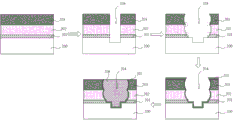
The specific process of forming the contact hole through the contact hole push-back (CT pullback) process, please refer to fig. 2, which includes: firstly, providing a device substrate 200 for completing the front-end process, and usually forming an etching stop layer 201 and an interlayer dielectric layer formed by stacking a plurality of film layers 202 and 203 on the surface thereof; then, longitudinally etching the interlayer dielectric layer, the etching stop layer 201 and the device substrate 200 with partial thickness in sequence to form a contact hole 204 in a straight hole form; then, a wet etching process is adopted to perform push-back etching (CT pullback) on the interlayer dielectric layer and the etching stop layer 201 on the side wall of the contact hole 204 to widen the contact hole 204 and expose part of the surface of the device substrate 200 at the bottom of the etching stop layer 201, thereby reducing the depth-to-width ratio of the contact hole 204; then, a layer of adhesion layer 205 (e.g., a Ti film and/or a TiN film) is covered in the contact hole 204, and the contact hole 204 is further filled with a conductive material to form a conductive plug 206.
In the contact hole push-back etching process, the sidewall coverage of the adhesion layer 205 is improved because the aspect ratio of the contact hole 204 is reduced, and the contact area between the adhesion layer 205 and the device substrate 200 is increased because the exposed surface of the device substrate 200 is increased, thereby reducing the contact resistance of the conductive plug 206 and improving the device performance. However, because the wet etching process is used to perform the push-back etching on the interlayer dielectric layer and the etching stop layer 201 on the sidewall of the contact hole 204, and the difference of the lateral etching rates of the wet etching process with respect to the etching stop layer 201 and the film layers 202 and 203 of the interlayer dielectric layer is large, a bump (tip, foot, which may be called a sharp corner, a tip, or a protrusion) may be formed at the boundary between each film layer of the interlayer dielectric layer and the boundary between the etching stop layer 201 and the interlayer dielectric layer, and the sidewalls of each film layer 202 and 203 of the interlayer dielectric layer may be in a certain arc shape, which may affect the deposition effect of the adhesion layer 205 on the sidewall of the contact hole 204, cause the problem that the adhesion layer 205 is easily peeled (peeling) from the sidewall of the contact hole 204, and affect the device performance.
Disclosure of Invention
The invention aims to provide a contact hole etching method and a semiconductor device manufacturing method, which can improve the appearance of a formed contact hole and further improve the performance of a device.
In order to achieve the above object, the present invention provides a method for etching a contact hole, comprising:
providing a substrate, and forming an interlayer dielectric layer on the substrate, wherein the interlayer dielectric layer comprises at least two dielectric film layers which are stacked up and down;
etching the interlayer dielectric layer and the substrate with partial thickness to form a straight hole exposing partial surface of the substrate;
performing back-push etching on the interlayer dielectric layer on the side wall of the straight hole to form a contact hole with a wide upper part and a narrow lower part, wherein the side wall of the interlayer dielectric layer exposed by the contact hole is uneven;
performing first-stage soft etching on the inner surface of the contact hole by using process gases including main etching gas, oxygen and inert gas to flatten the fluctuation of the side wall of the contact hole and increase the exposed area of the substrate;
and removing the oxygen and reducing the flow of the inert gas to adjust the process gas, and performing second-stage soft etching on the inner surface of the contact hole to smooth the inner surface of the contact hole.
Optionally, the main etching gas comprises a fluorocarbon gas and the inert gas comprises argon gas.
Optionally, the process gas further comprises carbon monoxide.
Optionally, the rf power of the etching tool is also reduced while adjusting the process gas.
Optionally, in the first-stage soft etching process, the etching selection ratio of the interlayer dielectric layer to the substrate is 8-10; and in the second stage soft etching process, the etching selection ratio of the interlayer dielectric layer to the substrate is more than 30.
Optionally, etching the interlayer dielectric layer and the substrate with a part of thickness by using a dry etching process to form the straight hole; and/or performing push-back etching on the interlayer dielectric layer on the side wall of the straight hole by adopting a wet etching process. Optionally, the substrate has at least one electrical structure, the electrical structure comprises at least one of an ion doping region, a grid electrode and a polysilicon resistor, the ion doping region comprises at least one of a source region, a drain region, a body region, a base region, a collector region and an emitter region, the ion doping region is formed in the surface layer of the substrate, and the contact hole exposes a part of the surface of the electrical structure.
Based on the same inventive concept, the invention also provides a manufacturing method of the semiconductor device, which comprises the following steps:
by adopting the contact hole etching method, a corresponding interlayer dielectric layer is formed on a substrate, and a contact hole exposing partial surface of the substrate is formed in the interlayer dielectric layer;
forming an adhesion layer on the surfaces of the interlayer dielectric layer and the contact hole;
and filling a conductive material in the contact hole to form a conductive plug.
Optionally, the interlayer dielectric layer includes a thermal oxidation layer, a phosphosilicate glass layer and a borophosphosilicate glass layer, which are sequentially covered on the surface of the substrate.
Optionally, the material of the adhesion layer comprises at least one of titanium, titanium nitride, tantalum nitride and metal silicide; the conductive material comprises at least one of copper, tungsten, nickel, aluminum and doped polysilicon.
Compared with the prior art, the technical scheme of the invention at least has the following beneficial effects:
after a straight hole is pushed back to a contact hole with a wide upper part and a narrow lower part through a conventional push-back etching process, firstly, the inner surface of the contact hole is subjected to first-stage soft etching by using process gas containing main etching gas and oxygen and having high inert gas flow, on the basis that the substrate surface at the bottom of the contact hole is hardly damaged, the fluctuation of the side wall of the contact hole is flattened, the exposed area of the substrate is effectively increased, then, the formula of the process gas is adjusted by removing the oxygen and reducing the inert gas flow, and the second-stage soft etching is continuously performed to trim and smooth the inner surface of the contact hole. Therefore, the deposition effect of the subsequent adhesion layer can be improved, the film thickness uniformity of the adhesion layer is improved, and the peeling problem of the adhesion layer is avoided, so that the contact resistance of the formed conductive plug is optimized, the performance of the device is greatly improved, and meanwhile, new defects are not introduced.
Detailed Description
The technical solution proposed by the present invention will be further described in detail with reference to fig. 3 to 8 and the specific embodiments. The advantages and features of the present invention will become more apparent from the following description. It is to be noted that the drawings are in a very simplified form and are not to precise scale, which is merely for the purpose of facilitating and distinctly claiming the embodiments of the present invention.
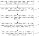
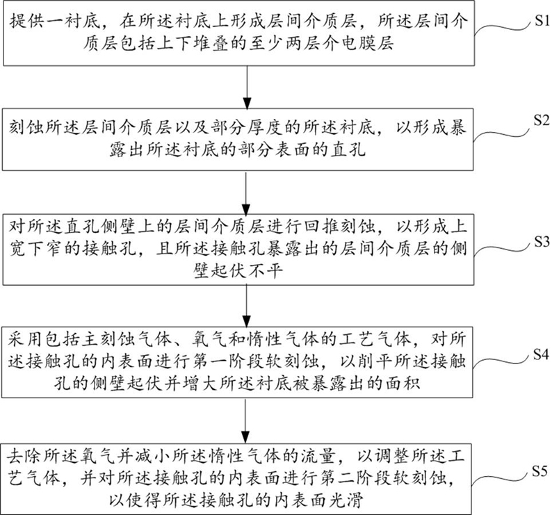
Referring to fig. 3, an embodiment of the invention provides a method for etching a contact hole, including the following steps:
s1, providing a substrate, and forming an interlayer dielectric layer on the substrate, wherein the interlayer dielectric layer comprises at least two dielectric film layers which are stacked up and down;
s2, etching the interlayer dielectric layer and the substrate with partial thickness to form a straight hole exposing partial surface of the substrate;
s3, performing push-back etching on the interlayer dielectric layer on the side wall of the straight hole to form a contact hole with a wide top and a narrow bottom, wherein the side wall of the interlayer dielectric layer exposed by the contact hole is uneven;
s4, adopting a process gas comprising a main etching gas, oxygen and an inert gas to carry out first-stage soft etching on the inner surface of the contact hole so as to flatten the side wall undulation of the contact hole and increase the exposed area of the substrate;
and S5, removing the oxygen and reducing the flow of the inert gas to adjust the process gas, and carrying out second-stage soft etching on the inner surface of the contact hole to make the inner surface of the contact hole smooth.
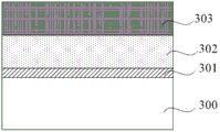
Referring to fig. 3 and 4, in step S1, a substrate 300 is first provided, where the substrate 300 may be any suitable substrate material known to those skilled in the art, such as monocrystalline silicon (Si), monocrystalline germanium (Ge), silicon germanium (GeSi), silicon carbide (SiC), silicon-on-insulator (SOI), germanium-on-insulator (GOI), gallium silicide, and other III-V compounds. The substrate 300 may be a device substrate having a front-end process, in which electrical structures such as gates, source regions, and drain regions of CMOS devices have been formed, or a device substrate having a back-end process, in which electrical structures such as gates, source regions, and drain regions of CMOS devices, and corresponding metal interconnects and conductive plugs have been formedAnd (5) structure. Then, an interlayer dielectric layer is formed on the substrate 300, wherein the interlayer dielectric layer is a laminated structure and comprises at least two dielectric film layers stacked up and down, and the material of the interlayer dielectric layer comprises silicon oxide and a low-K dielectric with the dielectric constant K lower than that of the silicon oxide. In this embodiment, the interlayer dielectric layer may include an etching stop layer 301 covering the substrate 300, a first dielectric film layer 302 on the etching stop layer 301, and a second dielectric film layer 303 on the first dielectric film layer 302, wherein the etching stop layer 301 is also a dielectric film layer, and the material thereof may be silicon oxide (SiO)2) Specifically, the etching stopper layer 301, the first dielectric film layer 302 and the second dielectric film layer 303 may be formed by a thermal oxidation process, and may be silicon nitride (SiN) or silicon carbonitride (SiCN), the first dielectric film layer 302 may be made of phosphosilicate glass (PSG) or fluorosilicate glass (FSG), the second dielectric film layer 303 may be made of borophosphosilicate glass (BPSG) or polyimide, and a thickness ratio of the etching stopper layer 301 to the first dielectric film layer 302 to the second dielectric film layer 303 is 200:6000: 5000. In other embodiments of the present invention, the interlayer dielectric layer is not limited to a three-layer structure, and may be a stacked structure of two, four, or more layers.
Referring to fig. 5, in step S2, a patterned photoresist (not shown) is formed on the interlayer dielectric layer, and a contact hole pattern is defined by the patterned photoresist; and etching the interlayer dielectric layer and the substrate 300 with a part of thickness by using the patterned photoresist as a mask through a plasma dry etching process to form a straight hole 304. In this embodiment, the straight hole 304 sequentially penetrates through the second dielectric film 303, the first dielectric film 302 and the etching stop layer 301 from top to bottom, and stops in a partial depth of the substrate 300. The main etching gas of the plasma dry etching process can comprise fluorocarbon gas such as carbon tetrafluoride and the like or hydrocarbon gas such as methane and the like, the formation of polymerization byproducts is controlled by adopting oxygen, and the physical bombardment is carried out by using argon as auxiliary gas. Optionally, the substrate 300 has at least one electrical structure (not shown) including at least one of an ion-doped region (not shown) formed in a surface layer of the substrate 300, the ion-doped region including at least one of a source region (not shown), a drain region (not shown), a body region (not shown), a base region (not shown), a collector region (not shown), and an emitter region (not shown), and the straight hole 304 exposes a portion of a surface of the electrical structure. In this step, the components of the polymerization by-product are mainly organic due to the presence of the patterned photoresist. The patterned photoresist formed in this step may be removed before step S3 is performed, after step S3 is performed and before step S4 is performed, or after step S5 is performed.
Referring to fig. 6, in step S3, a wet etching process is performed to push back the interlayer dielectric layer on the sidewall of the straight hole 304 to form a contact hole 304a with a wide top and a narrow bottom. The wet etching process not only pushes back the sidewall of the interlayer dielectric layer in the contact hole to a certain degree relative to the sidewall of the substrate 300, but also removes the polymerization by-products remained in the straight hole 304 in the step S2. In this step, because the material properties of the dielectric films (i.e., the etch stop layer 301, the first dielectric film 302, and the second dielectric film 303) in the interlayer dielectric layer are different, the wet etching process has a large difference in the etching rate for the dielectric films (i.e., the etch stop layer 301, the first dielectric film 302, and the second dielectric film 303) in the interlayer dielectric layer in the lateral direction, after the wet etching is completed, the protruding feet 303a are formed at the boundary between the adjacent dielectric films and at the boundary between the etch stop layer 301 and the substrate 300 on the sidewall of the contact hole 304a, and the curved surfaces 303b are formed on the sidewall of some dielectric films (e.g., the first dielectric film 302 and the second dielectric film 303) due to the large film thickness, so that the sidewall of the interlayer dielectric layer exposed by the contact hole 304a has uneven undulation.
Referring to fig. 6 and 7, in step S4, a first soft etching (soft etch) is performed on the inner surface of the contact hole 304a using a process gas including a main etching gas, oxygen and an inert gas to flatten the sidewall undulation of the contact hole 304a (i.e., remove the convex leg 303a and reduce the curvature of the arc 303 b), and since the convex leg of the etch stop layer 301 at the interface with the substrate 300 is removed, the size of the contact hole can be increasedThe exposed top surface area of the substrate 300. In step S5, the oxygen gas is removed and the flow of the inert gas is reduced to adjust the recipe of the process gas, so as to perform a second-stage soft etching (soft etch) on the inner surface of the contact hole 304a to smooth the inner surface of the contact hole 304 b. Wherein the main etching gas may include carbon tetrafluoride C4F8Equal fluorocarbon gas and/or methane CH4And (3) waiting for hydrocarbon gas, wherein the inert gas comprises argon and can provide certain ion bombardment to adjust the etching rate. In this embodiment, the process gas used in the first-stage soft etching and the second-stage soft etching further includes CO, which can improve the etching selectivity of the interlayer dielectric layer with respect to the substrate 300 during the soft etching process in the first-stage soft etching and the second-stage soft etching, and reduce the rf power of the etching machine while adjusting the formula of the process gas. Optionally, in the first-stage soft etching process, an etching selection ratio of the interlayer dielectric layer to the substrate 300 is 8-10; in the second stage soft etching process, the etching selection ratio of the interlayer dielectric layer to the substrate 300 is greater than 30.
Please refer to fig. 6 to 7, in this embodiment, step S4 and step S5 adopt two different stages of substantially the same etching process and the same process recipe, that is, the first stage soft etching of step S4 and the second stage soft etching of step S5 are performed in the same etching chamber of the same etching machine, and the adopted main etching gas and inert gas are the same. In this embodiment, since the fluorocarbon gas or the hydrocarbon gas is used as the main etching gas in step S4 and step S5, polymerization byproducts are formed in the soft etching process in both stages, and the components of the polymerization byproducts depend on the etching gas, the material of the interlayer dielectric layer, and the presence or absence of the photoresist on the interlayer dielectric layer, and may be organic (polymer), inorganic, or a combination of organic and inorganic. In step S4, in order to avoid the situation that the etching is stopped due to excessive generation of polymeric byproducts or the polymeric byproducts cannot be removed cleanly in the subsequent steps, resulting in a high contact resistance in the contact hole, a conventional soft etching method is used as a first stage soft etching, so as to smooth the undulation of the side wall of the contact hole on the one hand and substantially remove the redundant interlayer dielectric layer in the back etching region at the bottom of the contact hole on the other hand. In step S5, the process gas used in the first stage is adjusted to remove oxygen and reduce argon, so as to greatly increase the formation of polymerization byproducts, effectively protect the stability of the critical dimension of the etch-back region of the contact hole, greatly improve the selectivity of the interlayer dielectric layer to the substrate 300, reduce ion damage and almost eliminate substrate loss, thereby making the bottom of the contact hole 304b smooth in morphology, stable in resistance, and smooth and flat in sidewall. And the time of the second stage soft etching in step S5 needs to be set reasonably, which may cause the etching to stop if the time is too long, and the polymeric byproduct (polymer) is deposited seriously, and is difficult to remove later, which causes the resistance in the contact hole to be too high, and the time is too short, which may cause the substrate loss to increase, the substrate surface damage to be large, and the bottom junction of the step formed on the substrate 300 may easily form a pit, which may cause the contact resistance in the contact hole to fluctuate, and affect the device performance. In this embodiment, the time of the second-stage soft etching in step S5 is shorter than the time of the first-stage soft etching in step S4, for example, when the time of the first-stage soft etching in step S4 is more than 5S, for example, about 10S, and the time of the second-stage soft etching in step S5 is less than 10S.
Through the combination of the step S4 and the step S5, on the basis of maintaining the interlayer dielectric layer to have a higher etching selection ratio relative to the substrate 300 and ensuring low damage of the substrate 300, the characteristic of anisotropic etching in the soft etching process is enhanced, the side wall convex foot and arc surface morphology caused by film layer difference and wet method rate difference on the side wall of the contact hole is eliminated or greatly improved, and the stripping (peeling) defect possibly occurring in the subsequent deposition of the adhesion layer is solved, so that the contact area of the substrate and the adhesion layer can be effectively increased, the contact resistance is optimized, the device performance is greatly improved, and the defect of the conventional contact hole pushback etching process is avoided.
In addition, it should be noted that the soft etching in step S4 and step S5 in this embodiment is different from the conventional soft etching, which generally reduces the damage to the substrate 300 by obtaining a high etching selectivity of the dielectric film layer at the bottom of the contact hole to the etching stop layer (e.g., the first dielectric film layer 302 to the etching stop layer 301), and generally uses a process recipe with low power and a high etching selectivity of the dielectric film layer at the bottom of the contact hole to the etching stop layer, but without the etching stop layer, the substrate 300 is damaged strongly when the interlayer dielectric layer is etched, while the soft etching in step S4 and step S5 in this embodiment is equivalent to the optimization of the conventional soft etching, which increases the etching selectivity between the interlayer dielectric layer (i.e., the etching stop layer) and the substrate by changing the process recipe of the conventional soft etching, on the basis of not damaging the substrate as much as possible, the contact hole with smooth side wall and no convex foot, difficult peeling of the adhesion layer and no tip at the bottom of the contact hole is formed in the interlayer dielectric layer formed by stacking the multiple dielectric film layers (including the etching stop layers).
Referring to fig. 3 to 8, based on the same inventive concept, the present invention further provides a method for manufacturing a semiconductor device, including:
first, by using the contact hole etching method of the present invention, a corresponding interlayer dielectric layer is formed on a substrate 300, and a contact hole 304b exposing a part of the surface of the substrate 300 is formed in the interlayer dielectric layer, as an example, the interlayer dielectric layer includes a thermal oxide layer (i.e., an etch stop layer 301), a first dielectric film layer (e.g., a phosphosilicate glass layer) 302, and a second dielectric film layer (e.g., a borophosphosilicate glass layer) 303 sequentially covering the surface of the substrate 300;
then, an adhesion layer 305 is formed on the upper surface of the interlayer dielectric layer (i.e., the second dielectric film layer 303) and the inner surface of the contact hole 304b by a deposition process or the like, wherein the material of the adhesion layer 305 includes at least one of titanium, titanium nitride, tantalum nitride, and metal silicide;
next, a conductive material is filled in the contact hole 304b by a plating process or the like, and a top surface of the deposited conductive material is polished by a chemical mechanical polishing process until a top surface of the interlayer dielectric layer (i.e., the second dielectric film layer 303) is exposed, so as to form a conductive plug 306. Optionally, the conductive material comprises at least one of copper, tungsten, nickel, aluminum, doped polysilicon.
In summary, in the contact hole etching method and the semiconductor device manufacturing method of the present invention, after the straight hole is pushed back into the contact hole with a wide top and a narrow bottom by the conventional push-back etching process, the first stage soft etching is performed on the inner surface of the contact hole by using the process gas containing the main etching gas and the oxygen and having a high inert gas flow rate, on the basis of hardly damaging the substrate surface at the bottom of the contact hole, the unevenness of the sidewall of the contact hole is smoothed, the exposed area of the substrate is effectively increased, then the oxygen is removed and the inert gas flow rate is reduced to adjust the formula of the process gas, and the second stage soft etching is continued to trim the inner surface of the contact hole smoothly. Therefore, the deposition effect of the subsequent adhesion layer can be improved, the film thickness uniformity of the adhesion layer is improved, and the peeling problem of the adhesion layer is avoided, so that the contact resistance of the formed conductive plug is optimized, the performance of the device is greatly improved, and meanwhile, new defects are not introduced.
The above description is only for the purpose of describing the preferred embodiments of the present invention, and is not intended to limit the scope of the present invention, and any variations and modifications made by those skilled in the art according to the above disclosure are within the scope of the present invention.