Groove MOSFET device with NPN sandwich gate structure
Technical Field
The invention relates to the technical field of power semiconductor devices, in particular to a trench MOSFET device with an NPN sandwich gate structure.
Background
With the development of power electronic systems, power semiconductor devices are widely applied to important fields such as transportation, military defense, energy conversion and the like, and become important research hotspots in the academic world gradually. The power MOS device is an important component of a power semiconductor device, and has the advantages of high input impedance, high switching speed, low transient loss and the like, so that the power MOS device plays a leading role in a low-voltage power switching circuit. Due to application requirements, power MOSFET devices in low voltage applications are gradually beginning to develop along the trends of reducing device switching power consumption, increasing device current capability, and enhancing device reliability.
In order to improve the withstand voltage of the device, the power MOSFET device has undergone continuous development from a lateral structure to a longitudinal structure, from a planar structure to a trench structure. The Trench structure has undergone the development from the conventional Trench Gate MOSFET device to the step Oxide Trench MOSFET (RSO MOSFET) that reduces the surface electric field, and then to the Split-Gate Trench MOSFET (SGT MOSFET). The traditional groove gate MOSFET device mainly forms a gate electrode through deep groove etching and polysilicon deposition, and compared with the traditional plane gate, the traditional groove gate MOSFET device can effectively reduce the on-resistance of the device and improve the breakdown voltage of the device. The RSO MOSFET device is further optimized in a mode that the groove extends into the epitaxial layer drift region on the basis of the traditional groove gate MOSFET, the gate electrode extending into the drift region plays a role of an in-vivo field plate, the current carriers in the drift region are subjected to auxiliary depletion, and therefore the electric field of the drift region is effectively optimized, the RSO MOSFET device can achieve higher concentration of the drift region on the premise of the same breakdown voltage, and therefore the RSO MOSFET device has lower specific on-resistance. However, although the RSO MOSFET can achieve lower static loss, the RSO MOSFET has a large gate capacitance due to its large gate area, resulting in a large switching power loss when applied to a switching circuit.
In order to further optimize the performance of the trench-gate MOSFET, an SGT MOSFET device is proposed based on the conventional trench-gate MOSFET and RSO MOSFET, and the structural diagram is shown in fig. 1. Compared with the traditional groove gate MOSFET, the groove of the SGT MOSFET is deeper; compared with an RSO MOSFET, the grid electrode and the shielding grid of the SGT MOSFET are isolated through a medium, and meanwhile, the shielding grid electrode of the device is in short circuit with the source electrode in the three-dimensional front-back direction through the layout. The SGT MOSFET structure has two directional improvements over the two structures mentioned above: on one hand, the shielding grid can be used as an in-vivo field plate buried in a body to perform auxiliary depletion on a current carrier of the drift region, so that the depletion capability of the drift region of the device is effectively improved, and the electric field distribution of the drift region is optimized, so that the SGT MOSFET is ensured to have lower specific on-resistance on the premise of the same breakdown voltage; on the other hand, the overlapping area between the grid electrode and the drain electrode of the device is greatly reduced due to the existence of the shielding grid, so that the interelectrode capacitance between the grid electrode and the drain electrode can be effectively shielded, the grid-drain capacitance of the device is greatly reduced, the switching speed of the power MOSFET device is improved to a certain extent, and the switching loss of the device is reduced. However, the existing structure can convert the gate-drain capacitance into the source-drain capacitance, so that the input capacitance of the device is increased; secondly, the electric field distribution of the drift region of the structure still has certain heterogeneity, so that the improvement effect of the structure on the on-resistance is weakened; meanwhile, the structure needs to be subjected to deposition of an oxide layer for many times in the process preparation, so that certain process complexity is increased.
Disclosure of Invention
The invention aims to provide a trench MOSFET device with an NPN sandwich gate structure, which is improved on the basis of an SGT MOSFET and further improves the switching characteristic of a power MOSFET device.
In order to realize the purpose, the following technical scheme is adopted:
a trench MOSFET device with an NPN sandwich gate structure comprises a cell structure, wherein the cell structure comprises drain metal, an N + substrate, an N-type drift region and source metal which are sequentially stacked from bottom to top; a groove grid structure is formed on one side of the upper surface of the N-type drift region, and the groove grid structure comprises an N + Poly grid, a P-type lightly doped region and an N-type source contact region which are sequentially arranged from top to bottom; a P-type base region adjacent to the trench gate structure is arranged on the other side of the upper surface of the N-type drift region; the upper surface of the P-type base region is provided with an N-type heavily doped region and a P-type heavily doped region which are mutually contacted, and the N-type heavily doped region is arranged close to the trench gate structure; and the lower surface, the side surface and the upper surface of the trench gate structure are respectively provided with an oxide layer for isolating the N-type drift region, the P-type base region, the N-type heavily doped region and the source metal.
Preferably, the oxide layer between the side surfaces of the P-type lightly doped region and the N-type source contact region and the N-type drift region is a thick oxide layer, and the oxide layer on the side surface of the N + Poly gate is a thin oxide layer.
Preferably, the N-type source contact region is connected with the source metal.
The N + Poly grid, the P-type lightly doped region and the N-type source contact region jointly form an NPN sandwich structure in the groove, the auxiliary effect on the depletion of the drift region is enhanced, and meanwhile the influence between the grids and the shields of the drain electrode can be further reduced, so that the grid-drain capacitance of the device is reduced.
Compared with the traditional shielded gate trench MOSFET, the method effectively reduces the deposition times of the oxide layer in the trench gate, simplifies the layout design steps of the device and improves the design efficiency.
By adopting the scheme, the invention has the beneficial effects that:
the invention provides a trench MOSFET device with an NPN sandwich gate structure on the basis of the traditional shielded gate trench MOSFET structure, which utilizes the NPN sandwich structure in a trench gate to: on one hand, the depletion of the drift region can be realized, and the realization of higher doping concentration under the condition that the withstand voltage is not influenced is ensured, so that the specific on-resistance and the static loss of the device are reduced; on the other hand, the structure can also reduce the overlapping between the grid and the drain, thereby reducing the grid leakage capacitance, and simultaneously providing other current paths for the displacement current, thereby reducing the charging influence of the displacement current on the grid, effectively reducing the charging phenomenon of grid charges, and realizing faster switching speed and smaller switching loss.
Drawings
FIG. 1 is a schematic diagram of a prior art shielded gate trench MOSFET device in a lateral cross-sectional configuration;
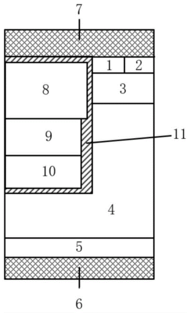
FIG. 2 is a schematic cross-sectional view of the present invention;
wherein the figures identify the description:
1-N type heavily doped region, 2-P type heavily doped region,
3-P type base region, 4-N type drift region,
5-N + substrate, 6-drain metal,
7-source metal, 8-N + Poly gate,
9-P type lightly doped region, 10-N type source contact region,
11-oxide layer.
Detailed Description
The embodiments of the present invention are described below with reference to specific embodiments, and other advantages and effects of the present invention will be easily understood by those skilled in the art from the disclosure of the present specification. The invention is capable of other and different embodiments and of being practiced or of being carried out in various ways, and its several details are capable of modification in various respects, all without departing from the spirit and scope of the present invention.
In order to further improve the static characteristics and the switching characteristics of the device and reduce the complexity of the process, the invention provides a trench MOSFET device with an NPN sandwich gate structure based on the existing SGT MOSFET structure, as shown in fig. 2. The main improvement of the structure is that: on one hand, the depletion of the drift region is further assisted by utilizing the depletion of a PN junction in the groove gate, and the electric field distribution in the drift region is optimized; on the other hand, the junction capacitance of the PN junction is utilized to further shield the grid electrode and the drain electrode, so that smaller grid-drain capacitance is realized, the switching speed of the device is improved, and the switching loss of the device is reduced.
The technical scheme of the invention is described in detail in the following with the accompanying drawings:
referring to fig. 2, the invention provides a trench MOSFET device with an NPN sandwich gate structure, which includes a cell structure, where the cell structure includes a drain metal 6, an N + substrate 5, an N-type drift region 4, and a source metal 7, which are sequentially stacked from bottom to top; a trench gate structure is formed on one side of the upper surface of the N-type drift region 4, and the trench gate structure comprises an N + Poly gate 8, a P-type lightly doped region 9 and an N-type source contact region 10 which are sequentially arranged from top to bottom; the other side of the upper surface of the N-type drift region 4 is provided with a P-type base region 3 adjacent to the trench gate structure; the upper surface of the P-type base region 3 is provided with an N-type heavily doped region 1 and a P-type heavily doped region 2 which are mutually contacted, and the N-type heavily doped region 1 is arranged close to the trench gate structure; and the lower surface, the side surface and the upper surface of the trench gate structure are respectively provided with an oxide layer 11 for isolating the N-type drift region 4, the P-type base region 3, the N-type heavily doped region 1 and the source metal 7.
An oxide layer 11 between the side surfaces of the P-type lightly doped region 9 and the N-type source contact region 10 and the N-type drift region 4 is a thick oxide layer, and an oxide layer 11 on the side surface of the N + Poly gate 8 is a thin oxide layer. The N-type source contact region 10 is connected to the source metal 7.
The principle of the invention is as follows: on the basis of an SGT MOSFET structure, an NPN sandwich structure is arranged in a groove to further optimize the effect of a shielding gate, wherein an N-type heavily doped region 1 in the NPN structure is led out as a poly gate, an N-type lightly doped region is floated, and an N-type source contact region 10 is connected with a source. Compared with the traditional SGT MOSFET device, the Trench MOSFET device (Split-Gate MOSFET with NPN Sandwich, SSGT MOSFET) with the NPN Sandwich structure enhances the shielding effect between the grid and the drain, greatly reduces the grid-drain capacitance of the device, and simultaneously leads the source-drain capacitance of the new structure to be far smaller than the source-drain capacitance of the traditional SGT MOSFET device due to the existence of smaller junction capacitance in the Trench grid NPN Sandwich structure in the new structure, and leads the output capacitance of the new structure to be far smaller than the output capacitance of the traditional structure due to the improvement of the grid-drain capacitance and the source-drain capacitance by the NPN Sandwich structure, thereby effectively improving the switching speed and the switching loss of the device. Meanwhile, the NPN sandwich structure in the groove gate realizes the improvement from the in-vivo resistance field plate to the in-vivo junction field plate, and can enhance the auxiliary effect of the groove structure on depletion, thereby further optimizing the internal electric field and the on-resistance of the drift region.
In summary, on the basis of the conventional shielded Gate Trench MOSFET structure, a Trench MOSFET device (a Split-Gate Trench MOSFET with an NPN Sandwich, SSGT MOSFET) having an NPN Sandwich structure is provided in a Trench, so that the electric field and specific on-resistance of the drift region in the body can be further optimized while the Gate-drain capacitance and the source-drain capacitance of the device are reduced, thereby achieving faster switching speed and lower static loss and switching loss.
The present invention is not limited to the above preferred embodiments, and any modifications, equivalent substitutions and improvements made within the spirit and principle of the present invention should be included in the protection scope of the present invention.