CN112242597B - Miniaturized high-selectivity wide-stop-band-pass filter based on multi-layer PCB structure - Google Patents
Miniaturized high-selectivity wide-stop-band-pass filter based on multi-layer PCB structure Download PDFInfo
- Publication number
- CN112242597B CN112242597B CN202011442107.3A CN202011442107A CN112242597B CN 112242597 B CN112242597 B CN 112242597B CN 202011442107 A CN202011442107 A CN 202011442107A CN 112242597 B CN112242597 B CN 112242597B
- Authority
- CN
- China
- Prior art keywords
- resonator
- metal plate
- layer
- plate layer
- metal
- Prior art date
- Legal status (The legal status is an assumption and is not a legal conclusion. Google has not performed a legal analysis and makes no representation as to the accuracy of the status listed.)
- Active
Links
- 239000002184 metal Substances 0.000 claims abstract description 140
- 229910052751 metal Inorganic materials 0.000 claims abstract description 140
- 230000008878 coupling Effects 0.000 claims abstract description 62
- 238000010168 coupling process Methods 0.000 claims abstract description 62
- 238000005859 coupling reaction Methods 0.000 claims abstract description 62
- 239000000758 substrate Substances 0.000 claims abstract description 23
- 238000006880 cross-coupling reaction Methods 0.000 abstract description 5
- 230000000694 effects Effects 0.000 abstract description 3
- 239000010410 layer Substances 0.000 description 120
- RYGMFSIKBFXOCR-UHFFFAOYSA-N Copper Chemical compound [Cu] RYGMFSIKBFXOCR-UHFFFAOYSA-N 0.000 description 20
- 229910052802 copper Inorganic materials 0.000 description 20
- 239000010949 copper Substances 0.000 description 20
- 230000005540 biological transmission Effects 0.000 description 9
- 238000005516 engineering process Methods 0.000 description 9
- 238000010586 diagram Methods 0.000 description 8
- 230000004044 response Effects 0.000 description 8
- 230000007547 defect Effects 0.000 description 6
- 239000012790 adhesive layer Substances 0.000 description 5
- 238000013461 design Methods 0.000 description 5
- 230000005855 radiation Effects 0.000 description 4
- 230000002829 reductive effect Effects 0.000 description 4
- 238000010897 surface acoustic wave method Methods 0.000 description 4
- 239000000919 ceramic Substances 0.000 description 3
- 238000004891 communication Methods 0.000 description 3
- 230000005684 electric field Effects 0.000 description 3
- 238000010030 laminating Methods 0.000 description 3
- 238000012545 processing Methods 0.000 description 3
- 230000009286 beneficial effect Effects 0.000 description 2
- 230000008859 change Effects 0.000 description 2
- 238000003780 insertion Methods 0.000 description 2
- 230000037431 insertion Effects 0.000 description 2
- 230000010354 integration Effects 0.000 description 2
- 239000000463 material Substances 0.000 description 2
- 230000036961 partial effect Effects 0.000 description 2
- 230000002093 peripheral effect Effects 0.000 description 2
- 230000004075 alteration Effects 0.000 description 1
- 230000002238 attenuated effect Effects 0.000 description 1
- 238000005452 bending Methods 0.000 description 1
- 239000003990 capacitor Substances 0.000 description 1
- 238000006243 chemical reaction Methods 0.000 description 1
- 230000002349 favourable effect Effects 0.000 description 1
- 239000012939 laminating adhesive Substances 0.000 description 1
- 238000011031 large-scale manufacturing process Methods 0.000 description 1
- 230000000670 limiting effect Effects 0.000 description 1
- 238000004519 manufacturing process Methods 0.000 description 1
- 238000010295 mobile communication Methods 0.000 description 1
- 238000012986 modification Methods 0.000 description 1
- 230000004048 modification Effects 0.000 description 1
- 230000010355 oscillation Effects 0.000 description 1
- 238000004806 packaging method and process Methods 0.000 description 1
- 230000000717 retained effect Effects 0.000 description 1
- 238000004088 simulation Methods 0.000 description 1
- 239000002356 single layer Substances 0.000 description 1
- 238000006467 substitution reaction Methods 0.000 description 1
- 230000001629 suppression Effects 0.000 description 1
- 238000012546 transfer Methods 0.000 description 1
Images

Classifications
-
- H—ELECTRICITY
- H01—ELECTRIC ELEMENTS
- H01P—WAVEGUIDES; RESONATORS, LINES, OR OTHER DEVICES OF THE WAVEGUIDE TYPE
- H01P1/00—Auxiliary devices
- H01P1/20—Frequency-selective devices, e.g. filters
Landscapes
- Control Of Motors That Do Not Use Commutators (AREA)
Abstract
The invention relates to the field of filters, in particular to a miniaturized high-selectivity wide-stop-band-pass filter based on a multi-layer PCB structure, which comprises five metal plate layers, four medium substrate layers, three prepreg bonding layers and a metal shielding assembly, wherein a first feed port and a second feed port are arranged on the first metal plate layer, the first metal plate layer is positioned on the bottommost layer, a first resonator and a fourth resonator are arranged on the second metal plate layer, a first square coupling window and a second square coupling window are arranged on the third metal plate layer, a second resonator and a third resonator are arranged on the fourth metal plate layer, the fifth metal plate layer is positioned on the topmost layer, and spatial coupling or direct coupling is realized through proper position arrangement among different resonators in the horizontal direction so as to achieve the effect of main path coupling or cross coupling; the size of the square coupling window is controlled in the vertical direction to realize the strength of energy coupling between different couplers.
Description
Technical Field
The invention belongs to the field of filters, and particularly relates to a miniaturized high-selectivity wide-stop-band-pass filter based on a multi-layer PCB structure.
Background
The filter is used as an indispensable important device in a radio frequency circuit and a wireless communication system, the performance of the filter determines the performance and the quality of the whole microwave system, the band-pass filter is used as an important branch of the filter, is a main component of signal selection and interference suppression in the microwave system, is widely applied to the aspects of mobile communication, integrated circuits and the like, and the band-pass filters commonly used at present are roughly divided into lumped element band-pass filters, metal cavity band-pass filters, microstrip line band-pass filters, Substrate Integrated Waveguide (SIW) band-pass filters, low temperature co-fired ceramic technology (LTCC) based band-pass filters, Surface Acoustic Wave (SAW) band-pass filters and the like according to the structure of the filter. The lumped element band-pass filter is characterized in that the lumped element capacitor and the inductor are respectively connected in series in a main circuit and in parallel in a branch circuit to form a transmission poleTransmission zeros are finally cascaded together to build a band pass response. The metal cavity body band-pass filter is characterized in that an electric wall formed by metal binds an electromagnetic signal in a closed cavity body, and the electromagnetic wave oscillates in the metal cavity body. The electromagnetic wave at the resonance frequency is retained and the electromagnetic waves of the remaining frequencies are attenuated in the oscillation, thereby constructing a band-pass response. The microstrip line band-pass filter utilizes the distribution parameter characteristics of microstrip lines to construct a resonator, and controls the coupling coefficient in a direct coupling or space coupling mode through the position arrangement between the microstrip lines, so that band-pass response is constructed. The substrate integrated waveguide band-pass filter utilizes metallized through holes to replace electric walls on the left and right narrow sides of the waveguide, and integrates the whole structure on a printed circuit board, TE between the same or different cavitiesnoThe modes couple to each other to build a band pass response. Based on a low temperature co-fired ceramic (LTCC) band-pass filter, the characteristics of multilayer circuit layout and high-density packaging of the LTCC technology are utilized, and multilayer layout and high-density integration are carried out on a distributed parameter circuit inside an LTCC substrate, so that band-pass response is constructed. The surface acoustic wave band-pass filter is used for performing mutual conversion on an electric signal and an acoustic signal by utilizing the positive and negative piezoelectric effects of the piezoelectric substrate and designing a proper transfer function so as to construct band-pass response; with the overall progress of communication technologies represented by 5G, there is a strong demand for a miniaturized high-performance bandpass filter satisfying N78 frequency bands (3300 MHz to 3800 MHz) at 6GHz or less.
The conventional lumped element band-pass filter has the defects of difficult application to high frequency and the like; the metal cavity band-pass filter is limited by a metal structure and has the defects of large volume, heavy mass, inflexible design and the like; the microstrip line band-pass filter is positioned in an open space, and has the defects of large radiation loss, easy interference with other circuit elements and interference by other elements; the substrate integrated waveguide band-pass filter is limited by a resonance principle and has the defect of relatively large volume; the low-temperature co-fired ceramic technology band-pass filter is limited by a processing technology and has the defects of high cost and the like; the surface acoustic wave band-pass filter has the defects of relatively large insertion loss, difficulty in being applied to high frequency and high power and the like.
Disclosure of Invention
The invention provides a miniaturized high-selectivity wide-stop-band-pass filter based on a multi-layer PCB structure, which aims to solve the problems that: the structure comprises five metal plate layers, four dielectric substrate layers, three prepreg bonding layers and a metal shielding assembly, wherein a first feed port and a second feed port are arranged on the first metal plate layer, the first metal plate layer is positioned on the bottommost layer, a first resonator and a fourth resonator are arranged on the second metal plate layer, a first square coupling window and a second square coupling window are arranged on the third metal plate layer, a second resonator and a third resonator are arranged on the fourth metal plate layer, and the fifth metal plate layer is positioned on the topmost layer; a first metal wire is connected to the first resonator and is connected with the first feed port through a first metal column, a second metal wire is connected to the fourth resonator and is connected with the second feed port through a second metal column; the second resonator and the third resonator are connected through a third metal wire; the first metal wire is connected with the first metal plate layer and the fifth metal plate layer simultaneously through a third metal column, the second metal wire is connected with the first metal plate layer and the fifth metal plate layer simultaneously through a fourth metal column, and the third metal wire is connected with the first metal plate layer and the fifth metal plate layer simultaneously through a fifth metal column; the prepreg bonding layer is used for connecting the medium substrate layer and the metal plate layer.
Preferably, the metal shielding component comprises a plurality of uniformly distributed metallized through holes, and the metallized through holes penetrate through the first metal plate layer to the fifth metal plate layer.
Preferably, the first resonator, the second resonator, the third resonator and the fourth resonator are all quarter-wavelength short-circuit stepped-impedance resonators.
Preferably, the first metal wire, the second metal wire and the third metal wire are all bent.
Preferably, the first feeding port and the second feeding port are coplanar waveguide type feeding ports.
Preferably, the first resonator and the second resonator are respectively disposed at corresponding positions of the second metal plate layer and the fourth metal plate layer, and the first square coupling window is disposed at corresponding positions of the first resonator and the second resonator.
Preferably, the third resonator and the fourth resonator are respectively disposed at corresponding positions of the fourth metal plate layer and the second metal plate layer, and the second square coupling window is disposed at corresponding positions of the third resonator and the fourth resonator.
The invention has the following beneficial effects: the miniaturized high-selectivity wide-stop-band-pass filter based on the multilayer PCB structure is provided, and space coupling or direct coupling is realized by arranging proper positions among different resonators in the horizontal direction so as to achieve the effect of main path coupling or cross coupling; the size of the square coupling window is controlled in the vertical direction to realize the strength of energy coupling between different couplers. The cross coupling and the source load coupling are realized, four transmission zeros are introduced to two sides of the passband, the selectivity of the band-pass filter is improved, the out-of-band rejection is improved, and the stop band performance is improved.
Drawings
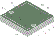
FIG. 1 is a schematic diagram of a main body structure of a filter according to an embodiment of the present invention;
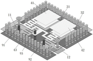
FIG. 2 is a schematic diagram of the overall structure of a filter according to an embodiment of the present invention;
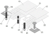
FIG. 3 is a schematic diagram of a partial structure of a filter according to an embodiment of the present invention;
FIG. 4 is a schematic diagram of a partial structure of a filter according to an embodiment of the present invention;
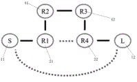
FIG. 5 is a diagram of the coupling topology of a filter in an embodiment of the present invention;
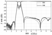
FIG. 6 is a schematic diagram of the frequency response of a filter according to an embodiment of the invention.
10-a first metal sheet layer; 11-a first feeding port; 12-a second feeding port; 20-a second metal sheet layer; 21-a first resonator; 22-a fourth resonator; 30-a third metal sheet layer; 31-a first square coupling window; 32-a second square coupling window; 40-a fourth metal sheet layer; 41-a second resonator; 42-a third resonator; 43-a third metal wire; 44-a first metal wire; 45-a second metal wire; 50-a fifth metal ply; 60-a dielectric substrate layer; 70-a prepreg adhesive layer; 80-metallized vias; 91-a third metal pillar; 92-a fourth metal pillar; 93-fifth metal column; 94-first metal pillar; 95-second metal posts.
Detailed Description
The technical solutions in the embodiments of the present invention will be clearly and completely described below with reference to the drawings in the embodiments of the present invention, and it is obvious that the described embodiments are only a part of the embodiments of the present invention, and not all of the embodiments. Unless otherwise specified, the technical means used in the examples are conventional means well known to those skilled in the art.
In the description of the present invention, it is to be understood that the terms "longitudinal", "lateral", "upper", "lower", "front", "rear", "left", "right", "vertical", "horizontal", "top", "bottom", "inner", "outer", and the like, indicate orientations or positional relationships based on those shown in the drawings, are merely for convenience of description of the present invention, and do not indicate or imply that the referenced devices or elements must have a particular orientation, be constructed and operated in a particular orientation, and thus, are not to be construed as limiting the present invention.
As shown in fig. 1 to 6, the miniaturized high-selectivity wide-stop-band-pass filter based on the multi-layer PCB structure includes five metal plate layers, four dielectric substrate layers 60, three prepreg adhesive layers 70 and a metal shielding assembly, a first feed port 11 and a second feed port 12 are disposed on a first metal plate layer 10, the first metal plate layer 10 is located at the bottommost layer, a first resonator 21 and a fourth resonator 22 are disposed on a second metal plate layer 20, a first square coupling window 31 and a second square coupling window 32 are disposed on a third metal plate layer 30, a second resonator 41 and a third resonator 42 are disposed on a fourth metal plate layer 40, and a fifth metal plate layer 50 is located at the topmost layer; a first metal wire 44 is connected to the first resonator 21, the first metal wire 44 is connected to the first feeding port 11 through a first metal post 94, a second metal wire 45 is connected to the fourth resonator 22, and the second metal wire 45 is connected to the second feeding port 12 through a second metal post 95; the second resonator 41 and the third resonator 42 are connected by a third metal wire 43; the first metal wire 44 is connected to the first metal plate layer 10 and the fifth metal plate layer 50 through a third metal pillar 91, the second metal wire 45 is connected to the first metal plate layer 10 and the fifth metal plate layer 50 through a fourth metal pillar 92, and the third metal wire 43 is connected to the first metal plate layer 10 and the fifth metal plate layer 50 through a fifth metal pillar 93; the prepreg adhesive layer 70 is used to connect the dielectric substrate layer 60 and the metal plate layer.
The filter is composed of four layers of dielectric substrates (substrate _ layer _01, substrate _ layer _02, substrate _ layer _03, substrate _ layer _ 04), five layers of metal plates (copper _ layer _01, copper _ layer _02, copper _ layer _03, copper _ layer _04, copper _ layer _ 05), three layers of prepreg adhesive layers 70 (pp _ layer _01, pp _ layer _02, pp _ layer _ 03), four quarter-wavelength short step impedance resonators (R1, R2, R3, R4), a square coupling window, a metalized via 80, a coplanar waveguide feed port, and the like. The four-layer dielectric substrate is used for serving copper layers on the upper part and the lower part of the substrate as supporting materials; a three-layer prepreg bonding layer 70, which functions as a laminating adhesive to bond the four-layer dielectric substrate; the metal plate layers of the top layer (copper _ layer _ 05) and the bottom layer (copper _ layer _ 01), preferably the metal plate layers are metal copper layers, which are used as the floor of the filter and are connected with the peripheral metalized through holes 80 to form a metal shielding cavity, so that the radiation loss is reduced, and the electromagnetic compatibility of the device is improved; inner three metal plate layers (coupler _ layer _02, coupler _ layer _03 and coupler _ layer _ 04) for placing resonators and square coupling windows; the four quarter-wavelength short-circuit step impedance resonators are bent for reducing the size, and have the function of expanding the distance between the first harmonic and the fundamental wave of the resonators by utilizing impedance nonuniformity, so that the characteristic of a wide stop band of the filter is realized; a square coupling window for controlling the strength of energy coupling between the first resonator 21 and the second resonator 41, and between the third resonator 42 and the fourth resonator 22 in the vertical direction by controlling the size of the coupling window; the coplanar waveguide type feed port is used as an input and output port of energy, and is convenient for integrating the band-pass filter in a microwave circuit.
A novel miniaturized and low-loss band-pass filter implementation mode is provided based on a miniaturized high-selectivity wide-stop-band-pass filter of a multi-layer PCB structure, namely, a vertical-direction space is fully utilized by utilizing a multi-layer PCB laminating technology, and the miniaturized design is realized; meanwhile, a metal shielding cavity is constructed, so that the electromagnetic compatibility of the band-pass filter is improved while the radiation loss is reduced. The first feed port 11, i.e. the coplanar waveguide feed port, at the bottom most layer (copper _ layer _ 01) feeds energy into the filter, which is transferred along the metallized via 80 to the first resonator 21 at the second layer metal plate layer (copper _ layer _ 02). All resonators are quarter-wavelength short-circuit step impedance resonators, the size of the microstrip line is adjusted according to an equivalent RLC circuit of the transmission line, the change of the value of the equivalent LC is achieved, the change of the resonant frequency of the filter can be achieved, and meanwhile, the distance between the first harmonic and the fundamental wave of the resonators can be adjusted by changing the step impedance ratio of the resonators. The first resonator 21 vertically couples energy to the second resonator 41 located at (coupler _ layer _ 04) of the fourth layer of metal plate layer through the first square coupling window 31 located at the third layer of metal plate layer (coupler _ layer _ 03). The size of the square coupling window is used to control the strength of the spatial energy coupling. The second resonator 41 and the third resonator 42 located on the fourth metal plate layer (coupler _ layer _ 04) perform energy transmission through direct coupling (magnetic coupling). The third resonator 42 vertically couples energy to the fourth resonator 22 on the second layer of metallic copper layer (copper _ layer _ 02) again through the second square coupling window 32 on the third layer of metallic plate layer (copper _ layer _ 03), and finally feeds energy out through the metalized via 80 through the second feed port 12, i.e., the coplanar waveguide output port, located on the lowest layer of metallic copper layer (copper _ layer _ 01), thereby implementing a fourth order chebyshev bandpass filter design. The first resonator 21 and the fourth resonator 22 located in the second metal plate layer (coupler _ layer _ 02) also introduce weak cross coupling through spatial coupling, so that two sides of the passband each generate a transmission zero. At the same time, source-load coupling (source-load coupling) also introduces a transmission zero on each side of the pass band. The introduction of the transmission zero point improves the selectivity of the band-pass filter, improves the out-of-band rejection and improves the out-of-band rejection degree.
The dielectric substrate material used by the band-pass filter is Rogers5580 with the thickness of 0.254 mm; the prepreg adhesive layer 70 was 0.1mm thick Ro4450F, the relative dielectric constant was 3.52, and the dielectric loss tangent was 0.004; the thickness of the metallic copper layer was 0.018 mm. The band-pass filter is designed to be N78 (3300 MHz-3800 MHz), the center frequency is 3.565GHz, -3dB bandwidth is 3.3 GHz-3.83 GHz, the relative bandwidth is 14.9%, the minimum insertion loss in the band is-1.866 dB, the rectangular coefficient is 0.57, and the 20dB out-of-band rejection of the upper stop band reaches 5.105f0. The size of the whole filter is 8.16mm × 7.91mm × 1.406mm (0.144 λ × 0.139 λ × 0.025 λ); the simulation output result is 3290 MHz-3820 MHz, and almost completely coincides with the N78 frequency band.
The multi-layer PCB laminating technology is adopted, after a micro-strip structure is constructed on a single-layer PCB substrate, the multi-layer PCB is laminated in the vertical direction, and the space in the vertical direction is fully utilized, so that the miniaturization design of the filter is realized. Compared with the conventional microstrip line filter, the microstrip line filter shortens the space in the horizontal direction, and can be better used for the design of a small microwave circuit. Compared with an LTCC filter, the LTCC filter does not need to be limited by a high-relative-dielectric-constant medium and a processing technology, the processing difficulty is reduced, and the manufacturing cost is saved. The filter can be directly applied to an integrated circuit, and only the feed port is directly welded, so that the filter has a good application prospect in a modern communication system.
The topmost metal plate layer (copper _ layer _ 05), the bottommost metal plate layer (copper _ layer _ 01) and the peripheral metalized via holes 80 are connected to form a metal shielding cavity. The structure of the metal shielding cavity reduces radiation loss and improves the electromagnetic compatibility of the band-pass filter.
In this filter, a quarter-wavelength short-circuited stepped-impedance resonator is used. The impedance nonuniformity of the filter is utilized to enlarge the distance between the first harmonic wave and the fundamental wave of the resonator, thereby realizing the characteristic of a wide stop band of the filter. Meanwhile, the bending is carried out, the size is further reduced, and the realization of miniaturization is facilitated.
Fig. 5 is a coupling topology diagram of the resonators, where the first resonator 21 and the fourth resonator 22 are in electric field coupling, the first resonator 21 and the second resonator 41 are in electric field coupling, the third resonator 42 and the fourth resonator 22 are in electric field coupling, the second resonator 41 and the third resonator 42 are in magnetic coupling, the first feed port 11, the first resonator 21 and the second feed port 12 are in magnetic coupling, and the fourth resonator 22 and the second feed port are in magnetic coupling, where coupling achieved through a square coupling window in the vertical direction is strong, and coupling achieved through a square coupling window in the horizontal direction is weak between the same layers.
Fig. 6 is a response diagram of the filter at 1-10GHz with a passband between 3290MHz and 3320MHz with four transmission zeroes, which is clearly seen to be excellent in out-of-band rejection.
The coupling between different resonators is realized by using square coupling windows. The strength of energy coupling between the resonators can be controlled by controlling the size of the square coupling window, and the coupling amount is not required to be changed by adjusting the positions of the resonators, so that the structure of the filter is more compact.
The characteristic that the input/output port and the bottommost metal plate layer (copper _ layer _ 01) are positioned on the same plane by adopting the coplanar waveguide type feed port enables the filter to be more easily integrated in a microwave circuit.
Cross coupling is introduced between the first resonator and the fourth resonator, source-load coupling is realized, and four transmission zeros are introduced on two sides of a pass band in total. The selectivity of the band-pass filter is improved, the out-of-band rejection is improved, and the out-of-band rejection degree is improved.
In conclusion, the band-pass filter has the characteristics of small size, low loss, high selectivity, wide stop band, easiness in integration of a microwave circuit and the like, and is favorable for being applied in scenes with small size and high performance requirements. The application of the multilayer PCB laminating technology is beneficial to reducing the cost and is suitable for large-scale production and application.
The above embodiments are merely illustrative of the preferred embodiments of the present invention, and do not limit the scope of the present invention, and those skilled in the art should make various changes, modifications, alterations, and substitutions on the technical solution of the present invention without departing from the spirit of the present invention, which falls within the protection scope defined by the claims of the present invention.
Claims (4)
1. Miniaturized high selectivity wide stop band pass filter based on multilayer PCB structure, its characterized in that: the structure comprises five metal plate layers, four dielectric substrate layers, three prepreg bonding layers and a metal shielding assembly, wherein a first feed port and a second feed port are arranged on the first metal plate layer, the first metal plate layer is positioned on the bottommost layer, a first resonator and a fourth resonator are arranged on the second metal plate layer, a first square coupling window and a second square coupling window are arranged on the third metal plate layer, a second resonator and a third resonator are arranged on the fourth metal plate layer, and the fifth metal plate layer is positioned on the topmost layer; a first metal wire is connected to the first resonator and is connected with the first feed port through a first metal column, a second metal wire is connected to the fourth resonator and is connected with the second feed port through a second metal column; the second resonator and the third resonator are connected through a third metal wire; the first metal wire is connected with the first metal plate layer and the fifth metal plate layer simultaneously through a third metal column, the second metal wire is connected with the first metal plate layer and the fifth metal plate layer simultaneously through a fourth metal column, and the third metal wire is connected with the first metal plate layer and the fifth metal plate layer simultaneously through a fifth metal column; the prepreg bonding layer is used for connecting the medium substrate layer and the metal plate layer;
the first resonator, the first square coupling window and the second resonator are correspondingly formed in the direction perpendicular to the metal plate layer, and the first resonator vertically couples energy to the second resonator through the first square coupling window; the third resonator, the second square coupling window and the fourth resonator are correspondingly formed in the direction perpendicular to the metal plate layer, and the third resonator vertically couples energy to the fourth resonator through the second square coupling window; the first resonator, the second resonator, the third resonator and the fourth resonator are all quarter-wavelength short-circuit step impedance resonators.
2. The miniaturized, highly selective, wide stop band bandpass filter based on multi-layer PCB structure of claim 1, wherein: the metal shielding assembly comprises a plurality of uniformly distributed metalized through holes, and the metalized through holes penetrate through the first metal plate layer to the fifth metal plate layer.
3. The miniaturized, highly selective, wide stop band bandpass filter based on multi-layer PCB structure of claim 1, wherein: the third metal wire is bent.
4. The miniaturized, highly selective, wide stop band bandpass filter based on multi-layer PCB structure of claim 1, wherein: the first feeding port and the second feeding port are coplanar waveguide type feeding ports.
Priority Applications (1)
| Application Number | Priority Date | Filing Date | Title |
|---|---|---|---|
| CN202011442107.3A CN112242597B (en) | 2020-12-11 | 2020-12-11 | Miniaturized high-selectivity wide-stop-band-pass filter based on multi-layer PCB structure |
Applications Claiming Priority (1)
| Application Number | Priority Date | Filing Date | Title |
|---|---|---|---|
| CN202011442107.3A CN112242597B (en) | 2020-12-11 | 2020-12-11 | Miniaturized high-selectivity wide-stop-band-pass filter based on multi-layer PCB structure |
Publications (2)
| Publication Number | Publication Date |
|---|---|
| CN112242597A CN112242597A (en) | 2021-01-19 |
| CN112242597B true CN112242597B (en) | 2021-04-06 |
Family
ID=74175265
Family Applications (1)
| Application Number | Title | Priority Date | Filing Date |
|---|---|---|---|
| CN202011442107.3A Active CN112242597B (en) | 2020-12-11 | 2020-12-11 | Miniaturized high-selectivity wide-stop-band-pass filter based on multi-layer PCB structure |
Country Status (1)
| Country | Link |
|---|---|
| CN (1) | CN112242597B (en) |
Families Citing this family (9)
| Publication number | Priority date | Publication date | Assignee | Title |
|---|---|---|---|---|
| CN112563699B (en) * | 2021-02-25 | 2021-05-11 | 成都频岢微电子有限公司 | Miniaturized spiral surface-mountable band-pass filter based on multilayer PCB structure |
| US11575189B1 (en) * | 2021-09-23 | 2023-02-07 | Hong Kong Applied Science And Technology Research Institute Co., Ltd | Multi-layer bandpass filter |
| CN114204236B (en) * | 2021-12-27 | 2022-10-21 | 井冈山大学 | Cavity double-frequency broadband filter with large frequency ratio |
| CN114295952B (en) * | 2021-12-30 | 2023-08-11 | 河北工业大学 | A non-contact voltage measurement method for dynamic voltage measurement of power devices |
| CN114566775B (en) * | 2022-03-07 | 2024-05-28 | 南京理工大学 | High-stop-band rejection microstrip band-stop filter applied to satellite communication |
| CN115207593B (en) * | 2022-06-13 | 2023-07-04 | 苏州博海创业微系统有限公司 | Multilayer dielectric resonator and dielectric filter |
| CN114899560B (en) * | 2022-06-21 | 2024-04-12 | 成都频岢微电子有限公司 | N79 frequency band miniaturized wide stop band filter based on LTCC technology |
| CN115189106B (en) * | 2022-06-29 | 2024-09-06 | 江苏江佳电子股份有限公司 | LTCC filter switch and wireless radio frequency front end |
| CN117895200B (en) * | 2024-03-11 | 2024-06-04 | 成都核心智慧科技有限公司 | 5G substrate integrated coaxial filter based on extraction pole resonator |
Citations (2)
| Publication number | Priority date | Publication date | Assignee | Title |
|---|---|---|---|---|
| JPH10276005A (en) * | 1997-03-28 | 1998-10-13 | Kyocera Corp | filter |
| CN103647122A (en) * | 2013-12-30 | 2014-03-19 | 陈日清 | Double-port vertical helical band-pass filter |
Family Cites Families (7)
| Publication number | Priority date | Publication date | Assignee | Title |
|---|---|---|---|---|
| JP4729464B2 (en) * | 2006-09-20 | 2011-07-20 | ルネサスエレクトロニクス株式会社 | Directional coupler and high-frequency circuit module |
| CN201243075Y (en) * | 2008-03-28 | 2009-05-20 | 深圳市麦捷微电子科技股份有限公司 | Lamination sheet type microwave band-pass filter |
| CN101640519B (en) * | 2009-09-02 | 2012-04-25 | 南京理工大学 | High stop-band inhibiting multi-zero 2.4 GHz mini filter |
| JP5936133B2 (en) * | 2011-01-28 | 2016-06-15 | 国立大学法人電気通信大学 | Transmission line resonator, bandpass filter using transmission line resonator, duplexer, balanced-unbalanced converter, power distributor, unbalanced-balanced converter, frequency mixer, and balanced filter |
| CN103035990A (en) * | 2012-12-12 | 2013-04-10 | 青岛联盟电子仪器有限公司 | Low Temperature Co-Fired Ceramic (LTCC) filter |
| CN103187603B (en) * | 2013-03-25 | 2015-11-11 | 华南理工大学 | A kind of Wide stop bands LTCC band pass filter based on magneto-electric coupled cancellation technology |
| US10033084B2 (en) * | 2014-11-10 | 2018-07-24 | The Regents Of The University Of California | Operation frequency band customizable and frequency tunable filters with EBG substrates |
-
2020
- 2020-12-11 CN CN202011442107.3A patent/CN112242597B/en active Active
Patent Citations (2)
| Publication number | Priority date | Publication date | Assignee | Title |
|---|---|---|---|---|
| JPH10276005A (en) * | 1997-03-28 | 1998-10-13 | Kyocera Corp | filter |
| CN103647122A (en) * | 2013-12-30 | 2014-03-19 | 陈日清 | Double-port vertical helical band-pass filter |
Non-Patent Citations (1)
| Title |
|---|
| High-Q Circular LTCC Resonator Using Zigzagged Via Posts and a λ/4 Short Stub for Millimeter-Wave System-on-Package Applications;Dong Yun Jung 等;《 IEEE Transactions on Advanced Packaging》;20090109;第32卷(第1期);第216-222页 * |
Also Published As
| Publication number | Publication date |
|---|---|
| CN112242597A (en) | 2021-01-19 |
Similar Documents
| Publication | Publication Date | Title |
|---|---|---|
| CN112242597A (en) | Miniaturized high-selectivity wide-stop-band-pass filter based on multi-layer PCB structure | |
| CN112563699B (en) | Miniaturized spiral surface-mountable band-pass filter based on multilayer PCB structure | |
| CN113346205B (en) | A Generalized Chebyshev Function Response Channel Continuous Identical Broadband Triplexer | |
| CN113708027A (en) | Capacitor loading type miniaturized 5G filter based on multilayer PCB structure | |
| CN112928409A (en) | Microstrip band-pass filter with wide stop band and high selectivity | |
| CN112164846A (en) | Millimeter wave band-pass filter | |
| CN118970408B (en) | Folding band-pass filter based on metal integrated suspension line structure | |
| CN107516753A (en) | A kind of wave filter based on the incomplete mould of substrate integration wave-guide | |
| CN114284664A (en) | Band-pass filter based on hybrid folded substrate integrated waveguide resonant cavity and novel stripline coupling | |
| US6091312A (en) | Semi-lumped bandstop filter | |
| CN113328223B (en) | Third-order band-pass filter | |
| US6064281A (en) | Semi-lumped bandpass filter | |
| CN119092956B (en) | Miniaturized low-loss LTCC millimeter wave band-pass filter | |
| CN116759779B (en) | 5G millimeter wave filtering power division module | |
| JPH05218705A (en) | Lamination type band elimination filter | |
| CN114899560B (en) | N79 frequency band miniaturized wide stop band filter based on LTCC technology | |
| CN112002974A (en) | Miniaturized SIW resonant cavity and wide-stop-band SIW filter formed by same | |
| JP3522098B2 (en) | Multilayer dielectric filter | |
| CN212725534U (en) | Miniaturized SIW resonant cavity and wide-stop-band SIW filter formed by same | |
| Yang et al. | Miniaturized, multilayer, shielded, and surface-mountable 5G N79 bandpass filter | |
| CN117913483B (en) | Band-pass filter with high selectivity and broadband suppression capability | |
| CN117914277B (en) | PCB structure of split type band-stop filter | |
| CN117895200B (en) | 5G substrate integrated coaxial filter based on extraction pole resonator | |
| CN119994425B (en) | Bandpass filter based on multilayer metal sheet waveguide | |
| CN119602734B (en) | Miniaturized ultra-wideband high-pass filter and notch filter integrated chip based on LTCC technology |
Legal Events
| Date | Code | Title | Description |
|---|---|---|---|
| PB01 | Publication | ||
| PB01 | Publication | ||
| SE01 | Entry into force of request for substantive examination | ||
| SE01 | Entry into force of request for substantive examination | ||
| GR01 | Patent grant | ||
| GR01 | Patent grant |