CN112281119A - Copper-cadmium-zinc-tin-selenium light absorption layer and preparation method thereof, and short-wave infrared detector - Google Patents

Copper-cadmium-zinc-tin-selenium light absorption layer and preparation method thereof, and short-wave infrared detector Download PDF

Info

Publication number
CN112281119A
CN112281119A CN202011039226.4A CN202011039226A CN112281119A CN 112281119 A CN112281119 A CN 112281119A CN 202011039226 A CN202011039226 A CN 202011039226A CN 112281119 A CN112281119 A CN 112281119A
Authority
CN
China
Prior art keywords
copper
substrate
cadmium
zinc
tin
Prior art date
Legal status (The legal status is an assumption and is not a legal conclusion. Google has not performed a legal analysis and makes no representation as to the accuracy of the status listed.)
Pending
Application number
CN202011039226.4A
Other languages
Chinese (zh)
Inventor
汪智伟
周长著
冯叶
黄建平
庞硕
黎年赐
杨春雷
Current Assignee (The listed assignees may be inaccurate. Google has not performed a legal analysis and makes no representation or warranty as to the accuracy of the list.)
Shenzhen Institute of Advanced Technology of CAS
Original Assignee
Shenzhen Institute of Advanced Technology of CAS
Priority date (The priority date is an assumption and is not a legal conclusion. Google has not performed a legal analysis and makes no representation as to the accuracy of the date listed.)
Filing date
Publication date
Application filed by Shenzhen Institute of Advanced Technology of CAS filed Critical Shenzhen Institute of Advanced Technology of CAS
Priority to CN202011039226.4A priority Critical patent/CN112281119A/en
Publication of CN112281119A publication Critical patent/CN112281119A/en
Pending legal-status Critical Current

Links

Images

Classifications

    • CCHEMISTRY; METALLURGY
    • C23COATING METALLIC MATERIAL; COATING MATERIAL WITH METALLIC MATERIAL; CHEMICAL SURFACE TREATMENT; DIFFUSION TREATMENT OF METALLIC MATERIAL; COATING BY VACUUM EVAPORATION, BY SPUTTERING, BY ION IMPLANTATION OR BY CHEMICAL VAPOUR DEPOSITION, IN GENERAL; INHIBITING CORROSION OF METALLIC MATERIAL OR INCRUSTATION IN GENERAL
    • C23CCOATING METALLIC MATERIAL; COATING MATERIAL WITH METALLIC MATERIAL; SURFACE TREATMENT OF METALLIC MATERIAL BY DIFFUSION INTO THE SURFACE, BY CHEMICAL CONVERSION OR SUBSTITUTION; COATING BY VACUUM EVAPORATION, BY SPUTTERING, BY ION IMPLANTATION OR BY CHEMICAL VAPOUR DEPOSITION, IN GENERAL
    • C23C14/00Coating by vacuum evaporation, by sputtering or by ion implantation of the coating forming material
    • C23C14/22Coating by vacuum evaporation, by sputtering or by ion implantation of the coating forming material characterised by the process of coating
    • C23C14/24Vacuum evaporation
    • CCHEMISTRY; METALLURGY
    • C23COATING METALLIC MATERIAL; COATING MATERIAL WITH METALLIC MATERIAL; CHEMICAL SURFACE TREATMENT; DIFFUSION TREATMENT OF METALLIC MATERIAL; COATING BY VACUUM EVAPORATION, BY SPUTTERING, BY ION IMPLANTATION OR BY CHEMICAL VAPOUR DEPOSITION, IN GENERAL; INHIBITING CORROSION OF METALLIC MATERIAL OR INCRUSTATION IN GENERAL
    • C23CCOATING METALLIC MATERIAL; COATING MATERIAL WITH METALLIC MATERIAL; SURFACE TREATMENT OF METALLIC MATERIAL BY DIFFUSION INTO THE SURFACE, BY CHEMICAL CONVERSION OR SUBSTITUTION; COATING BY VACUUM EVAPORATION, BY SPUTTERING, BY ION IMPLANTATION OR BY CHEMICAL VAPOUR DEPOSITION, IN GENERAL
    • C23C14/00Coating by vacuum evaporation, by sputtering or by ion implantation of the coating forming material
    • C23C14/06Coating by vacuum evaporation, by sputtering or by ion implantation of the coating forming material characterised by the coating material
    • C23C14/08Oxides
    • C23C14/086Oxides of zinc, germanium, cadmium, indium, tin, thallium or bismuth
    • CCHEMISTRY; METALLURGY
    • C23COATING METALLIC MATERIAL; COATING MATERIAL WITH METALLIC MATERIAL; CHEMICAL SURFACE TREATMENT; DIFFUSION TREATMENT OF METALLIC MATERIAL; COATING BY VACUUM EVAPORATION, BY SPUTTERING, BY ION IMPLANTATION OR BY CHEMICAL VAPOUR DEPOSITION, IN GENERAL; INHIBITING CORROSION OF METALLIC MATERIAL OR INCRUSTATION IN GENERAL
    • C23CCOATING METALLIC MATERIAL; COATING MATERIAL WITH METALLIC MATERIAL; SURFACE TREATMENT OF METALLIC MATERIAL BY DIFFUSION INTO THE SURFACE, BY CHEMICAL CONVERSION OR SUBSTITUTION; COATING BY VACUUM EVAPORATION, BY SPUTTERING, BY ION IMPLANTATION OR BY CHEMICAL VAPOUR DEPOSITION, IN GENERAL
    • C23C14/00Coating by vacuum evaporation, by sputtering or by ion implantation of the coating forming material
    • C23C14/06Coating by vacuum evaporation, by sputtering or by ion implantation of the coating forming material characterised by the coating material
    • C23C14/14Metallic material, boron or silicon
    • C23C14/18Metallic material, boron or silicon on other inorganic substrates
    • CCHEMISTRY; METALLURGY
    • C23COATING METALLIC MATERIAL; COATING MATERIAL WITH METALLIC MATERIAL; CHEMICAL SURFACE TREATMENT; DIFFUSION TREATMENT OF METALLIC MATERIAL; COATING BY VACUUM EVAPORATION, BY SPUTTERING, BY ION IMPLANTATION OR BY CHEMICAL VAPOUR DEPOSITION, IN GENERAL; INHIBITING CORROSION OF METALLIC MATERIAL OR INCRUSTATION IN GENERAL
    • C23CCOATING METALLIC MATERIAL; COATING MATERIAL WITH METALLIC MATERIAL; SURFACE TREATMENT OF METALLIC MATERIAL BY DIFFUSION INTO THE SURFACE, BY CHEMICAL CONVERSION OR SUBSTITUTION; COATING BY VACUUM EVAPORATION, BY SPUTTERING, BY ION IMPLANTATION OR BY CHEMICAL VAPOUR DEPOSITION, IN GENERAL
    • C23C14/00Coating by vacuum evaporation, by sputtering or by ion implantation of the coating forming material
    • C23C14/06Coating by vacuum evaporation, by sputtering or by ion implantation of the coating forming material characterised by the coating material
    • C23C14/14Metallic material, boron or silicon
    • C23C14/18Metallic material, boron or silicon on other inorganic substrates
    • C23C14/185Metallic material, boron or silicon on other inorganic substrates by cathodic sputtering
    • CCHEMISTRY; METALLURGY
    • C23COATING METALLIC MATERIAL; COATING MATERIAL WITH METALLIC MATERIAL; CHEMICAL SURFACE TREATMENT; DIFFUSION TREATMENT OF METALLIC MATERIAL; COATING BY VACUUM EVAPORATION, BY SPUTTERING, BY ION IMPLANTATION OR BY CHEMICAL VAPOUR DEPOSITION, IN GENERAL; INHIBITING CORROSION OF METALLIC MATERIAL OR INCRUSTATION IN GENERAL
    • C23CCOATING METALLIC MATERIAL; COATING MATERIAL WITH METALLIC MATERIAL; SURFACE TREATMENT OF METALLIC MATERIAL BY DIFFUSION INTO THE SURFACE, BY CHEMICAL CONVERSION OR SUBSTITUTION; COATING BY VACUUM EVAPORATION, BY SPUTTERING, BY ION IMPLANTATION OR BY CHEMICAL VAPOUR DEPOSITION, IN GENERAL
    • C23C14/00Coating by vacuum evaporation, by sputtering or by ion implantation of the coating forming material
    • C23C14/22Coating by vacuum evaporation, by sputtering or by ion implantation of the coating forming material characterised by the process of coating
    • C23C14/34Sputtering
    • C23C14/35Sputtering by application of a magnetic field, e.g. magnetron sputtering
    • CCHEMISTRY; METALLURGY
    • C23COATING METALLIC MATERIAL; COATING MATERIAL WITH METALLIC MATERIAL; CHEMICAL SURFACE TREATMENT; DIFFUSION TREATMENT OF METALLIC MATERIAL; COATING BY VACUUM EVAPORATION, BY SPUTTERING, BY ION IMPLANTATION OR BY CHEMICAL VAPOUR DEPOSITION, IN GENERAL; INHIBITING CORROSION OF METALLIC MATERIAL OR INCRUSTATION IN GENERAL
    • C23CCOATING METALLIC MATERIAL; COATING MATERIAL WITH METALLIC MATERIAL; SURFACE TREATMENT OF METALLIC MATERIAL BY DIFFUSION INTO THE SURFACE, BY CHEMICAL CONVERSION OR SUBSTITUTION; COATING BY VACUUM EVAPORATION, BY SPUTTERING, BY ION IMPLANTATION OR BY CHEMICAL VAPOUR DEPOSITION, IN GENERAL
    • C23C14/00Coating by vacuum evaporation, by sputtering or by ion implantation of the coating forming material
    • C23C14/22Coating by vacuum evaporation, by sputtering or by ion implantation of the coating forming material characterised by the process of coating
    • C23C14/54Controlling or regulating the coating process
    • CCHEMISTRY; METALLURGY
    • C23COATING METALLIC MATERIAL; COATING MATERIAL WITH METALLIC MATERIAL; CHEMICAL SURFACE TREATMENT; DIFFUSION TREATMENT OF METALLIC MATERIAL; COATING BY VACUUM EVAPORATION, BY SPUTTERING, BY ION IMPLANTATION OR BY CHEMICAL VAPOUR DEPOSITION, IN GENERAL; INHIBITING CORROSION OF METALLIC MATERIAL OR INCRUSTATION IN GENERAL
    • C23CCOATING METALLIC MATERIAL; COATING MATERIAL WITH METALLIC MATERIAL; SURFACE TREATMENT OF METALLIC MATERIAL BY DIFFUSION INTO THE SURFACE, BY CHEMICAL CONVERSION OR SUBSTITUTION; COATING BY VACUUM EVAPORATION, BY SPUTTERING, BY ION IMPLANTATION OR BY CHEMICAL VAPOUR DEPOSITION, IN GENERAL
    • C23C14/00Coating by vacuum evaporation, by sputtering or by ion implantation of the coating forming material
    • C23C14/58After-treatment
    • C23C14/5806Thermal treatment
    • CCHEMISTRY; METALLURGY
    • C23COATING METALLIC MATERIAL; COATING MATERIAL WITH METALLIC MATERIAL; CHEMICAL SURFACE TREATMENT; DIFFUSION TREATMENT OF METALLIC MATERIAL; COATING BY VACUUM EVAPORATION, BY SPUTTERING, BY ION IMPLANTATION OR BY CHEMICAL VAPOUR DEPOSITION, IN GENERAL; INHIBITING CORROSION OF METALLIC MATERIAL OR INCRUSTATION IN GENERAL
    • C23CCOATING METALLIC MATERIAL; COATING MATERIAL WITH METALLIC MATERIAL; SURFACE TREATMENT OF METALLIC MATERIAL BY DIFFUSION INTO THE SURFACE, BY CHEMICAL CONVERSION OR SUBSTITUTION; COATING BY VACUUM EVAPORATION, BY SPUTTERING, BY ION IMPLANTATION OR BY CHEMICAL VAPOUR DEPOSITION, IN GENERAL
    • C23C26/00Coating not provided for in groups C23C2/00 - C23C24/00
    • CCHEMISTRY; METALLURGY
    • C23COATING METALLIC MATERIAL; COATING MATERIAL WITH METALLIC MATERIAL; CHEMICAL SURFACE TREATMENT; DIFFUSION TREATMENT OF METALLIC MATERIAL; COATING BY VACUUM EVAPORATION, BY SPUTTERING, BY ION IMPLANTATION OR BY CHEMICAL VAPOUR DEPOSITION, IN GENERAL; INHIBITING CORROSION OF METALLIC MATERIAL OR INCRUSTATION IN GENERAL
    • C23CCOATING METALLIC MATERIAL; COATING MATERIAL WITH METALLIC MATERIAL; SURFACE TREATMENT OF METALLIC MATERIAL BY DIFFUSION INTO THE SURFACE, BY CHEMICAL CONVERSION OR SUBSTITUTION; COATING BY VACUUM EVAPORATION, BY SPUTTERING, BY ION IMPLANTATION OR BY CHEMICAL VAPOUR DEPOSITION, IN GENERAL
    • C23C28/00Coating for obtaining at least two superposed coatings either by methods not provided for in a single one of groups C23C2/00 - C23C26/00 or by combinations of methods provided for in subclasses C23C and C25C or C25D
    • C23C28/30Coatings combining at least one metallic layer and at least one inorganic non-metallic layer
    • C23C28/32Coatings combining at least one metallic layer and at least one inorganic non-metallic layer including at least one pure metallic layer
    • C23C28/321Coatings combining at least one metallic layer and at least one inorganic non-metallic layer including at least one pure metallic layer with at least one metal alloy layer
    • CCHEMISTRY; METALLURGY
    • C23COATING METALLIC MATERIAL; COATING MATERIAL WITH METALLIC MATERIAL; CHEMICAL SURFACE TREATMENT; DIFFUSION TREATMENT OF METALLIC MATERIAL; COATING BY VACUUM EVAPORATION, BY SPUTTERING, BY ION IMPLANTATION OR BY CHEMICAL VAPOUR DEPOSITION, IN GENERAL; INHIBITING CORROSION OF METALLIC MATERIAL OR INCRUSTATION IN GENERAL
    • C23CCOATING METALLIC MATERIAL; COATING MATERIAL WITH METALLIC MATERIAL; SURFACE TREATMENT OF METALLIC MATERIAL BY DIFFUSION INTO THE SURFACE, BY CHEMICAL CONVERSION OR SUBSTITUTION; COATING BY VACUUM EVAPORATION, BY SPUTTERING, BY ION IMPLANTATION OR BY CHEMICAL VAPOUR DEPOSITION, IN GENERAL
    • C23C28/00Coating for obtaining at least two superposed coatings either by methods not provided for in a single one of groups C23C2/00 - C23C26/00 or by combinations of methods provided for in subclasses C23C and C25C or C25D
    • C23C28/30Coatings combining at least one metallic layer and at least one inorganic non-metallic layer
    • C23C28/34Coatings combining at least one metallic layer and at least one inorganic non-metallic layer including at least one inorganic non-metallic material layer, e.g. metal carbide, nitride, boride, silicide layer and their mixtures, enamels, phosphates and sulphates
    • HELECTRICITY
    • H10SEMICONDUCTOR DEVICES; ELECTRIC SOLID-STATE DEVICES NOT OTHERWISE PROVIDED FOR
    • H10FINORGANIC SEMICONDUCTOR DEVICES SENSITIVE TO INFRARED RADIATION, LIGHT, ELECTROMAGNETIC RADIATION OF SHORTER WAVELENGTH OR CORPUSCULAR RADIATION
    • H10F77/00Constructional details of devices covered by this subclass
    • H10F77/10Semiconductor bodies
    • H10F77/12Active materials
    • H10F77/128Active materials comprising only Group I-II-IV-VI kesterite materials, e.g. Cu2ZnSnSe4 or Cu2ZnSnS4

Landscapes

  • Chemical & Material Sciences (AREA)
  • Chemical Kinetics & Catalysis (AREA)
  • Engineering & Computer Science (AREA)
  • Materials Engineering (AREA)
  • Mechanical Engineering (AREA)
  • Metallurgy (AREA)
  • Organic Chemistry (AREA)
  • Inorganic Chemistry (AREA)
  • Physics & Mathematics (AREA)
  • Thermal Sciences (AREA)
  • Light Receiving Elements (AREA)

Abstract

本发明公开了一种铜镉锌锡硒光吸收层的制备方法,其包括:提供基底置于共蒸镀腔室中,将基底加热至预定温度;在第一时间段内,使Cu、Zn、Cd、Sn和Se同时蒸发而蒸镀到基底上;在第二时间段内,使Zn、Cd、Sn和Se同时蒸发而蒸镀到基底上;在第三时间段内,使Sn和Se同时蒸发而蒸镀到基底上;在第四时间段内,使Se蒸发而蒸镀到基底上,冷却后获得蒸镀材料层;将蒸镀材料层进行退火处理,获得铜镉锌锡硒光吸收层。本发明还提供了如上制备方法获得的铜镉锌锡硒光吸收层以及包含该铜镉锌锡硒光吸收层的短波红外探测器。本发明可以使得铜镉锌锡硒光吸收层的晶粒更大而晶界减少,其应用于短波红外探测器中可以提高探测器的效率。

Figure 202011039226

The invention discloses a preparation method of a copper-cadmium-zinc-tin-selenium light absorption layer, which comprises the following steps: providing a substrate and placing it in a co-evaporation chamber, heating the substrate to a predetermined temperature; , Cd, Sn and Se are evaporated at the same time to be evaporated on the substrate; in the second time period, Zn, Cd, Sn and Se are evaporated at the same time to be evaporated to the substrate; in the third time period, Sn and Se are evaporated Simultaneously evaporate and deposit on the substrate; in the fourth time period, make Se evaporate and deposit on the substrate, and obtain an evaporation material layer after cooling; anneal the evaporation material layer to obtain copper cadmium zinc tin selenium light Absorbent layer. The invention also provides the copper-cadmium-zinc-tin-selenium light-absorbing layer obtained by the above preparation method and a short-wave infrared detector comprising the copper-cadmium-zinc-tin-selenium light-absorbing layer. The invention can make the crystal grains of the copper-cadmium-zinc-tin-selenium light absorption layer larger and the grain boundaries reduced, and the application of the invention in the short-wave infrared detector can improve the efficiency of the detector.

Figure 202011039226

Description

Copper-cadmium-zinc-tin-selenium light absorption layer, preparation method thereof and short-wave infrared detector
Technical Field
The invention belongs to the technical field of photoelectric detectors, and particularly relates to a copper-cadmium-zinc-tin-selenium light absorption layer and a preparation method thereof, and a short-wave infrared detector comprising the copper-cadmium-zinc-tin-selenium light absorption layer.
Background
The short wave infrared detector has wide application in the fields of industrial detection, civil monitoring, biology, medical treatment and the like. At present, commercial short-wave infrared detectors in the market are mainly indium gallium arsenic detectors, although the short-wave infrared detectors have good performance, the short-wave infrared detectors are low in material tolerance, required indium and gallium elements are expensive, production cost is high, and the process is harsh, so that the short-wave infrared detectors are mainly used in the fields of military affairs, aviation and the like and cannot be popularized for civil use. For this reason, some related technologies proposed copper cadmium zinc tin selenium (Cu)2CdxZn1-xSnSe4CCZTSe) as a light-absorbing layer for short-wave infrared detectionIn the detector, the elements required by the copper-cadmium-zinc-tin-selenium light absorption layer are abundant in natural reserves, the environmental pollution is low, the preparation process is relatively simple, the detection range covers visible light and infrared bands simultaneously, and compared with an indium-gallium-arsenic infrared detector, the copper-cadmium-zinc-tin-selenium light absorption layer has the advantages of low cost, simple process and easiness in large-scale production.
For a copper-cadmium-zinc-tin-selenium light absorption layer, the current preparation process comprises the following steps: (1) under the vacuum condition and at a lower temperature, co-evaporating Cu, Zn, Cd, Sn and Se elements on a substrate by adopting a one-step method to obtain a precursor material layer; (2) and annealing the precursor material layer at a higher temperature to obtain the copper-cadmium-zinc-tin-selenium light absorption layer. The copper cadmium zinc tin selenium light absorption layer obtained by the preparation process has the defect that crystal grains are too small and crystal boundaries are too large, and the problem that carriers are captured and compounded by the defect due to the fact that the crystal grains are too small and the crystal boundaries are too large in the light absorption layer is solved, so that the efficiency of a detector is low.
Disclosure of Invention
In view of the defects in the prior art, the invention provides a copper-cadmium-zinc-tin-selenium light absorption layer and a preparation method thereof, and aims to solve the problem that crystal grains in the copper-cadmium-zinc-tin-selenium light absorption layer are too small and crystal boundaries are too much in the prior art.
In order to achieve the purpose, the invention adopts the following technical scheme:
a preparation method of a copper-cadmium-zinc-tin-selenium light absorption layer comprises the following steps:
providing a substrate, placing the substrate in a co-evaporation chamber, and heating the substrate to a preset temperature;
in a first time period, evaporating Cu, Zn, Cd, Sn and Se simultaneously to evaporate the Cu, Zn, Cd, Sn and Se onto the substrate;
evaporating Zn, Cd, Sn and Se to be evaporated on the substrate at the same time in a second time period;
in a third time period, evaporating Sn and Se simultaneously to evaporate the Sn and the Se to the substrate;
in a fourth time period, evaporating Se to be evaporated on the substrate, and cooling to obtain an evaporation material layer;
and annealing the evaporation material layer to obtain the copper-cadmium-zinc-tin-selenium light absorption layer.
In a preferred scheme, the preset temperature is 360-420 ℃, and the annealing temperature for annealing the evaporation material layer is 140-260 ℃.
In a preferred scheme, the time of the first time period is 40min to 45min, the time of the second time period is 7min to 9min, the time of the third time period is 2min to 5min, and the time of the fourth time period is 4min to 7 min.
In a preferred scheme, in the first time period, the atomic ratio of evaporation of Cu to Sn is controlled to be (1.5-1.8): 1, and the atomic ratio of evaporation of Cu to evaporation of Zn and Cd is controlled to be (1.4-1.8): 1.
In a preferred scheme, the vacuum degree in the co-evaporation chamber is controlled to be 1.5 multiplied by 10 in the first time period to the fourth time period-5Pa~3.0×10⁻⁴Pa。
In a preferred embodiment, during the fourth time period, a NaF evaporation source is further provided, and NaF and Se are simultaneously evaporated and evaporated onto the substrate.
In a preferred scheme, in the fourth time period, firstly closing to stop evaporating NaF for 1-2 min, and then closing to stop evaporating Se.
In a preferred scheme, in the fourth time period, firstly closing to stop evaporating NaF for 1-2 min, then stopping heating the substrate to cool the substrate to below 300 ℃, and then closing to stop evaporating Se.
The invention also provides the copper-cadmium-zinc-tin-selenium light absorption layer prepared by the preparation method.
Another aspect of the present invention provides a short wave infrared detector, comprising:
a substrate;
a bottom electrode layer formed on the substrate;
a light absorbing layer formed on the bottom electrode layer; the light absorption layer is the copper cadmium zinc tin selenium light absorption layer;
a buffer layer formed on the light absorbing layer;
a window layer formed on the buffer layer; and the number of the first and second groups,
a top electrode layer formed on the window layer.
According to the preparation method of the copper-cadmium-zinc-tin-selenium light absorption layer, the co-evaporation method is adopted to evaporate Cu, Zn, Cd, Sn and Se elements to obtain an evaporation material layer (precursor material layer), a step-by-step evaporation process is adopted in the co-evaporation process to provide a precursor material growth process from copper-rich to copper-poor, so that larger crystal grains are obtained by precursor growth, and the copper-cadmium-zinc-tin-selenium light absorption layer with smaller crystal grains and less crystal boundaries can be obtained by annealing at lower temperature after the precursor material layer is obtained by evaporation. Furthermore, the copper-cadmium-zinc-tin-selenium light absorption layer is applied to a short-wave infrared detector, so that the problems of carrier capture and recombination by defects can be reduced, and the efficiency of the detector is improved.
Drawings
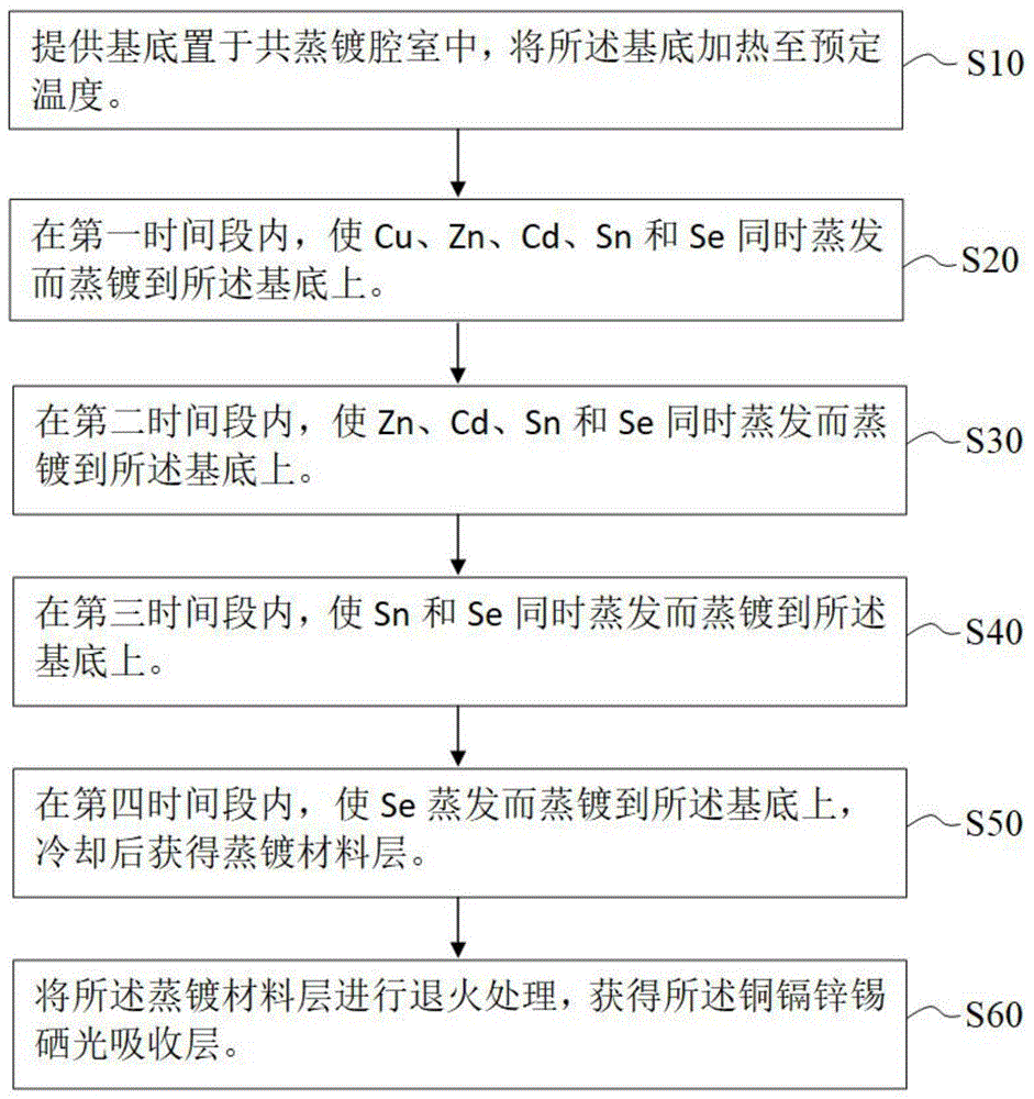
FIG. 1 is a process flow chart of a method for producing a CZTSSe light-absorbing layer in example 1 of the present invention;
FIG. 2 is an SEM of the CZTSSe light-absorbing layer in example 1 of the present invention;
FIG. 3 is an SEM of a Cu-Cd-Zn-Sn-Se light-absorbing layer of a comparative example of the present invention;
fig. 4 is a schematic structural diagram of a short-wave infrared detector in embodiment 2 of the present invention.
Detailed Description
In order to make the objects, technical solutions and advantages of the present invention more apparent, embodiments of the present invention are described in detail below with reference to the accompanying drawings. Examples of these preferred embodiments are illustrated in the accompanying drawings. The embodiments of the invention shown in the drawings and described in accordance with the drawings are exemplary only, and the invention is not limited to these embodiments.
It should be noted that, in order to avoid obscuring the present invention with unnecessary details, only the structures and/or processing steps closely related to the scheme according to the present invention are shown in the drawings, and other details not so relevant to the present invention are omitted.
Example 1
The embodiment provides a preparation method of a copper-cadmium-zinc-tin-selenium light absorption layer and the copper-cadmium-zinc-tin-selenium light absorption layer prepared by the method.
Referring to fig. 1, the method for preparing the copper-cadmium-zinc-tin-selenium light absorption layer according to the embodiment includes the following steps:
and S10, providing a substrate, placing the substrate in a co-evaporation chamber, and heating the substrate to a preset temperature.
In this embodiment, the substrate is a calcium glass substrate, and the co-evaporation equipment is Molecular Beam Epitaxy (MBE) vacuum coating equipment. It should be noted that, in other embodiments, the substrate may also be selected from other substrates commonly used in detectors, such as a silicon substrate; and when the light absorption layer to be prepared is applied to a detector, the substrate may refer to a substrate on which other functional structure layers (e.g., a bottom electrode) are prepared before the light absorption layer is grown. The co-evaporation equipment is provided with a Cu source, a Zn source, a Cd source, a Sn source and a Se source, each material source is provided with a baffle respectively, and whether a certain material is evaporated on a substrate or not is controlled by controlling the opening and closing of the baffle corresponding to the material source.
In this embodiment, the degree of vacuum in the chamber of the co-evaporation apparatus was controlled to 2 × 10⁻⁵Pa, heating said substrate to a predetermined temperature, in particular 360 ℃. It should be noted that in other embodiments, the vacuum degree in the co-evaporation chamber can be controlled to be 1.5 × 10⁻⁵Pa~3.0×10⁻⁴Pa, and the predetermined temperature may be selected to be in the range of 360 ℃ to 420 ℃.
And S20, evaporating Cu, Zn, Cd, Sn and Se to evaporate the Cu, Zn, Cd, Sn and Se to the substrate at the same time in the first time period.
Specifically, a Cu source, a Zn source, a Cd source, a Sn source and a Se source are preheated for 15-20 min to reach an evaporation condition, and then baffles corresponding to the Cu source, the Zn source, the Cd source, the Sn source and the Se source are opened, so that Cu, Zn, Cd, Sn and Se are evaporated at the same time and evaporated on the substrate.
In this embodiment, the time for evaporating and depositing Cu, Zn, Cd, Sn, and Se simultaneously is 45min, that is, the time of the first period of time is 45 min. It should be noted that, in some other embodiments, the time of the first period may be set in a range from 40min to 45 min.
In this embodiment, during the first period, the atomic ratio of Cu to Sn evaporation is controlled to be 1.6:1, and the atomic ratio of Cu to (Zn and Cd) evaporation is controlled to be 1.8: 1. In other embodiments, the atomic ratio of Cu to Sn evaporation may be controlled within a range of (1.5-1.8): 1, and the atomic ratio of Cu to (Zn and Cd) evaporation may be controlled within a range of (1.4-1.8): 1 during the first period.
And S30, evaporating Zn, Cd, Sn and Se to the substrate at the same time in a second time period.
Specifically, after step S20 is finished, the shutter corresponding to the Cu source is closed and the shutters corresponding to the Zn source, Cd source, Sn source and Se source are kept open, so that Zn, Cd, Sn and Se continue to evaporate simultaneously onto the substrate, whereby the growth process of the precursor is switched from the copper-rich phase to the copper-poor phase.
In this embodiment, the time for evaporating Zn, Cd, Sn, and Se simultaneously is 8min, that is, the time of the second period of time is 8 min. It should be noted that, in some other embodiments, the time of the second time period may be set within a range of 7min to 9 min.
And S40, evaporating Sn and Se simultaneously to evaporate the Sn and the Se to the substrate in a third time period.
Specifically, after step S30 ends, the shutters corresponding to the Zn source and the Cd source are turned off while the shutters corresponding to the Sn source and the Se source are kept on, so that Sn and Se continue to evaporate simultaneously to be evaporated onto the substrate, thereby continuing to replenish the Sn and Se elements.
In this embodiment, the time for evaporating Sn and Se simultaneously is 2min, that is, the time of the third period is 2 min. It should be noted that, in some other embodiments, the time of the third time period may be set within a range of 2min to 5 min.
And S50, evaporating Se to be evaporated on the substrate in a fourth time period, and cooling to obtain an evaporation material layer.
Specifically, after step S40 ends, the shutter corresponding to the Sn source is turned off while the shutter corresponding to the Se source is kept on, so that Se continues to evaporate and evaporate onto the substrate, thereby continuing to supplement the Se element.
In this embodiment, the time for continuing evaporation and deposition of Se is 6min, that is, the time for the fourth period of time is 6 min. It should be noted that, in some other embodiments, the time of the fourth time period may be set within a range of 4min to 7 min.
In this embodiment, a NaF evaporation source is further provided in the co-evaporation apparatus. And in the fourth time period, a baffle corresponding to the NaF source is also opened, so that NaF and Se are evaporated simultaneously and evaporated onto the substrate. By doping with alkali metals, the grain size of the material layer can be further increased.
In a preferred scheme, in the fourth time period, the NaF is closed to stop evaporating for 1-2 min and then the Se is closed to stop evaporating.
In a more preferable scheme, in the fourth time period, after the NaF is firstly closed and stopped evaporating for 1min to 2min, the substrate is stopped being heated and cooled to below 300 ℃, and then the Se is closed and stopped evaporating.
Specifically, in the present embodiment, during the fourth period of time, NaF and Se are simultaneously evaporated for 5min, then the shutter corresponding to the NaF source is turned off, then the heating of the substrate is stopped to cool the substrate to below 300 ℃, and finally the evaporation of Se is stopped after the shutter is turned off.
And S60, annealing the evaporation material layer to obtain the copper-cadmium-zinc-tin-selenium light absorption layer.
Specifically, the evaporation material layer formed in step S50 is cooled to room temperature and then taken out, and then placed in an annealing device for annealing at 160 ℃ for 2 min. It should be noted that, in other embodiments, the annealing temperature may be set within a range of 140 ℃ to 260 ℃, and the annealing time may be set within a range of 2min to 5 min.
Fig. 2 is an SEM image of the cdzn-sn-se light absorption layer prepared in this example, and as shown in fig. 2, the cdzn-sn-se light absorption layer of this example has larger crystal grains and fewer grain boundaries.
For comparison, in this example, the copper cadmium zinc tin selenium light absorption layer of the comparative example is prepared by referring to the process steps of the prior art, and the details are as follows:
(1) and co-evaporating Cu, Zn, Cd, Sn and Se on the substrate for 45min by adopting a one-step method under the condition that the substrate temperature is 200 ℃ to obtain a precursor material layer.
(2) And annealing the precursor material layer at the temperature of 500 ℃ for 2min to obtain the copper-cadmium-zinc-tin-selenium light absorption layer.
FIG. 3 is an SEM photograph of the Cu-Cd-Zn-Sn-Se light-absorbing layer of the comparative example above. As can be seen from comparison between fig. 2 and fig. 3, in the process of co-evaporating the precursor material layer, the embodiment of the present invention provides a growth process of a copper-rich to copper-poor precursor material by using a step-by-step evaporation process, so that the precursor grows to obtain larger grains, and the optical absorption layer (e.g., the CCZTSe layer in the figure) obtained after annealing has larger grains and fewer grain boundaries.
In the conventional process, the co-evaporation precursor material layer (1) is usually performed at a relatively low temperature (200 ℃ or lower), and the annealing temperature (2) is required to be performed at a relatively high temperature (usually 450 to 550 ℃) in order to obtain a high-quality light absorbing layer. Such a process also brings about the following problems:
when the copper cadmium zinc tin selenium light absorption layer is applied to a photodetector, such as a short-wave infrared detector, the device usually further includes a bottom layer circuit, and after the bottom layer circuit including a thin film transistor (such as a CMOS transistor) is formed, a structure of the photodetector is prepared on the bottom layer circuit, so that when the temperature of the annealing process in the step (2) is too high, the performance of the thin film transistor is degraded, and the performance of the detector is further adversely affected.
In the technical solution of the above embodiment of the present invention, in the step of co-evaporating the precursor material layer, the co-evaporation is performed at a relatively high temperature (as mentioned above, the temperature may be selected within a range of 360 ℃ to 420 ℃), and a growth process of a precursor material rich in copper to poor in copper is provided, so that a larger grain size is obtained in the precursor material, and thus, a subsequent annealing process may be performed at a relatively low temperature (as mentioned above, the temperature may be selected within a range of 140 ℃ to 260 ℃) to obtain a higher-quality light absorption layer, thereby avoiding degradation of the performance of the bottom layer circuit due to an excessively high annealing temperature, and being better compatible with the process of the bottom layer circuit.
Example 2
The embodiment provides a short-wave infrared detector and a preparation method thereof.
As shown in fig. 4, the short-wave infrared detector includes a substrate 1, and a bottom electrode layer 2, a light absorbing layer 3, a buffer layer 4, a window layer 5, and a top electrode layer 6 sequentially disposed on the substrate 1.
In this embodiment, the substrate 1 is a glass substrate, the bottom electrode layer 2 is a molybdenum electrode, the light absorption layer 3 is the cdzn-sn-se light absorption layer as described in embodiment 1, the buffer layer 4 is a CdS buffer layer, and the window layer 5 is made of a transparent conductive material (e.g., aluminum-doped zinc oxide (AZO)).
In this embodiment, the top electrode layer 6 is a grid electrode including a plurality of sub-electrodes 6a arranged at intervals. Since the window layer 5 of the transparent conductive material has a large area resistance and is not capable of effectively collecting electric charges, the electric charges can be collected more effectively by providing the gate electrode. In a preferred embodiment, the sub-electrode 6a may be configured to include a Ni metal layer, an Al metal layer, and a Ni metal layer sequentially disposed on the window layer 5, forming a Ni/Al/Ni electrode structure. In some other embodiments of the short wave infrared detector, the top electrode layer 6 may be omitted, and the charge collection capability may be improved by increasing the thickness of the window layer 5.
In the short-wave infrared detector of the embodiment, an intrinsic zinc oxide thin film layer (i-ZnO)7 is further arranged between the buffer layer 4 and the window layer 5.
The embodiment also provides a preparation method of the short wave infrared detector, which comprises the following steps:
firstly, a substrate 1 is provided, and a bottom electrode layer 2 is prepared and formed on the substrate 1.
Specifically, in this embodiment, the substrate 1 is selected to be a lime glass substrate, and the material of the bottom electrode layer 2 is molybdenum. The method comprises the steps of firstly cleaning the substrate 1 by using deionized water and a cleaning agent, drying the cleaned substrate 1 by using nitrogen, then baking the substrate 1 for a period of time, and then conveying the substrate 1 to a sputtering chamber. After the substrate 1 is placed in a sputtering chamber, a bottom electrode layer 2 is manufactured on the substrate 1 by adopting a direct current magnetron sputtering process, and the specific process is as follows: molybdenum is adopted as a target material, (1.1), and the molybdenum is circularly sputtered on a substrate 1 for 8 times under the argon atmosphere with the air pressure of 1Pa and the sputtering power of 300W; (1.2) and then, the substrate was subjected to cyclic sputtering at a sputtering power of 800W for 4 times in an argon atmosphere at a pressure of 0.2Pa to prepare a bottom electrode layer 2 having a thickness of 500 nm.
In some further embodiments: the air pressure in the step 1.1 can be set within the range of 1 Pa-3 Pa, and the sputtering power is within the range of 300W-400W; the gas pressure in the step 1.2 may be set in a range of 0.2 to 0.4Pa, and the sputtering power may be set in a range of 800 to 1200W.
And secondly, preparing and forming a copper cadmium zinc tin selenium light absorption layer 3 on the bottom electrode layer 2.
Specifically, referring to the process of example 1, a copper cadmium zinc tin selenium light absorption layer 3 is formed on the bottom electrode layer 2.
And thirdly, preparing and forming a CdS buffer layer 4 on the copper-cadmium-zinc-tin-selenium light absorption layer 3 by applying a chemical water bath deposition process. In this embodiment, the reaction solution of the chemical water bath deposition process is a mixed solution of cadmium sulfate, ammonia water, and thiourea, the reaction temperature is set to 69 ℃, and the reaction time is 10 min.
Fourthly, preparing and forming an intrinsic zinc oxide film layer 7 on the CdS buffer layer 4.
Specifically, in this embodiment, the intrinsic zinc oxide layer 7 is deposited on the buffer layer 4 by using radio frequency magnetron sputtering. The specific process can be as follows: and sputtering the ZnO as a target material on the CdS buffer layer 4 under a vacuum condition at a power of 120W to form an intrinsic zinc oxide layer 7 with a thickness of 250 nm.
And fifthly, preparing and forming a window layer 5 on the intrinsic zinc oxide film layer 7.
Specifically, in this embodiment, the window layer 5 is deposited on the intrinsic zinc oxide thin film layer 7 by using radio frequency magnetron sputtering. The specific process can be as follows: and sputtering Al and ZnO as targets on the intrinsic zinc oxide film layer 7 under a vacuum condition at 750W to form a window layer 5 with the thickness of 200 nm.
And S60, preparing and forming a top electrode layer 6 on the window layer 5.
In this embodiment, a Ni metal layer, an Al metal layer, and a Ni metal layer are sequentially deposited on the window layer 5, and then a gate electrode including a plurality of sub-electrodes 6a arranged at intervals is formed by an etching process, and each sub-electrode 6a is formed as an electrode structure of Ni/Al/Ni, respectively.
According to the short-wave infrared detector provided by the embodiment of the invention, the light absorption layer is the copper-cadmium-zinc-tin-selenium light absorption layer with large crystal grains and few crystal boundaries, so that the problems of carrier capture and recombination by defects can be reduced, and the efficiency of the detector is improved.
The foregoing is directed to embodiments of the present application and it is noted that numerous modifications and adaptations may be made by those skilled in the art without departing from the principles of the present application and are intended to be within the scope of the present application.

Claims (10)

1.一种铜镉锌锡硒光吸收层的制备方法,其特征在于,包括:1. a preparation method of copper cadmium zinc tin selenium light absorption layer, is characterized in that, comprises: 提供基底置于共蒸镀腔室中,将所述基底加热至预定温度;providing a substrate to be placed in a co-evaporation chamber, and heating the substrate to a predetermined temperature; 在第一时间段内,使Cu、Zn、Cd、Sn和Se同时蒸发而蒸镀到所述基底上;During a first period of time, Cu, Zn, Cd, Sn, and Se are simultaneously evaporated to be evaporated onto the substrate; 在第二时间段内,使Zn、Cd、Sn和Se同时蒸发而蒸镀到所述基底上;During a second period of time, Zn, Cd, Sn and Se are simultaneously evaporated to evaporate onto the substrate; 在第三时间段内,使Sn和Se同时蒸发而蒸镀到所述基底上;During a third time period, Sn and Se are simultaneously evaporated and deposited onto the substrate; 在第四时间段内,使Se蒸发而蒸镀到所述基底上,冷却后获得蒸镀材料层;In the fourth time period, the Se is evaporated to be evaporated on the substrate, and the evaporation material layer is obtained after cooling; 将所述蒸镀材料层进行退火处理,获得所述铜镉锌锡硒光吸收层。The evaporation material layer is annealed to obtain the copper-cadmium-zinc-tin-selenium light absorption layer. 2.根据权利要求1所述的铜镉锌锡硒光吸收层的制备方法,其特征在于,所述预定温度为360℃~420℃,所述将所述蒸镀材料层进行退火处理的退火温度为140℃~260℃。2 . The method for preparing a copper-cadmium-zinc-tin-selenium light absorbing layer according to claim 1 , wherein the predetermined temperature is 360° C.˜420° C., and the annealing process of annealing the vapor deposition material layer is performed. 3 . The temperature is 140℃~260℃. 3.根据权利要求1所述的铜镉锌锡硒光吸收层的制备方法,其特征在于,所述第一时间段的时间为40min~45min,所述第二时间段的时间为7min~9min,所述第三时间段的时间为2min~5min,所述第四时间段的时间为4min~7min。3. The preparation method of copper-cadmium-zinc-tin-selenium light absorption layer according to claim 1, wherein the time of the first time period is 40min~45min, and the time of the second time period is 7min~9min , the time of the third time period is 2 min to 5 min, and the time of the fourth time period is 4 min to 7 min. 4.根据权利要求1所述的铜镉锌锡硒光吸收层的制备方法,其特征在于,在第一时间段内,控制Cu与Sn蒸发的原子比为(1.5~1.8):1,控制Cu与Zn和Cd蒸发的原子比为(1.4~1.8):1。4. the preparation method of copper-cadmium-zinc-tin-selenium light absorption layer according to claim 1, is characterized in that, in the first period of time, the atomic ratio of controlling Cu and Sn evaporation is (1.5~1.8): 1, controlling The atomic ratio of Cu to Zn and Cd evaporation is (1.4~1.8):1. 5.根据权利要求1所述的铜镉锌锡硒光吸收层的制备方法,其特征在于,在第一时间段至第四时间段内,控制所述共蒸镀腔室中的真空度为1.5×10⁻⁵Pa~3.0×10⁻⁴Pa。5 . The method for preparing a copper-cadmium-zinc-tin-selenium light absorbing layer according to claim 1 , wherein, in the first time period to the fourth time period, the vacuum degree in the co-evaporation chamber is controlled to be: 6 . 1.5×10 -5 Pa~3.0×10 -4 Pa. 6.根据权利要求1-5任一所述的铜镉锌锡硒光吸收层的制备方法,其特征在于,在第四时间段内,还提供NaF蒸发源,使NaF和Se同时蒸发而蒸镀到所述基底上。6. according to the preparation method of the arbitrary described copper-cadmium-zinc-tin-selenium light absorption layer of claim 1-5, it is characterized in that, in the fourth time period, also provide NaF evaporation source, make NaF and Se evaporate simultaneously and evaporate onto the substrate. 7.根据权利要求6所述的铜镉锌锡硒光吸收层的制备方法,其特征在于,在第四时间段内,先关闭停止蒸发NaF 1min~2min后再关闭停止蒸发Se。7 . The method for preparing a copper-cadmium-zinc-tin-selenium light absorbing layer according to claim 6 , wherein in the fourth time period, the evaporation of NaF is turned off for 1 to 2 minutes, and then the evaporation of Se is turned off. 8 . 8.根据权利要求7所述的铜镉锌锡硒光吸收层的制备方法,其特征在于,在第四时间段内,先关闭停止蒸发NaF 1min~2min后,停止加热所述基底使其冷却至300℃以下后,再关闭停止蒸发Se。8 . The method for preparing a copper-cadmium-zinc-tin-selenium light absorbing layer according to claim 7 , wherein, in the fourth time period, after turning off and stopping NaF evaporating for 1 min to 2 min, the substrate is stopped from heating to cool it. 9 . After the temperature is below 300°C, it is turned off again to stop evaporating Se. 9.如权利要求1-8任一所述的制备方法制备获得的铜镉锌锡硒光吸收层。9. The copper-cadmium-zinc-tin-selenium light absorption layer prepared by the preparation method according to any one of claims 1-8. 10.一种短波红外探测器,其特征在于,包括:10. A short-wave infrared detector, characterized in that, comprising: 衬底;substrate; 形成于所述衬底上的底电极层;a bottom electrode layer formed on the substrate; 形成于所述底电极层上的光吸收层;所述光吸收层为如权利要求9所述的铜镉锌锡硒光吸收层;a light absorbing layer formed on the bottom electrode layer; the light absorbing layer is the copper cadmium zinc tin selenium light absorbing layer as claimed in claim 9; 形成于所述光吸收层上的缓冲层;a buffer layer formed on the light absorbing layer; 形成于所述缓冲层上的窗口层;以及,a window layer formed on the buffer layer; and, 形成于所述窗口层上的顶电极层。a top electrode layer formed on the window layer.
CN202011039226.4A 2020-09-28 2020-09-28 Copper-cadmium-zinc-tin-selenium light absorption layer and preparation method thereof, and short-wave infrared detector Pending CN112281119A (en)

Priority Applications (1)

Application Number Priority Date Filing Date Title
CN202011039226.4A CN112281119A (en) 2020-09-28 2020-09-28 Copper-cadmium-zinc-tin-selenium light absorption layer and preparation method thereof, and short-wave infrared detector

Applications Claiming Priority (1)

Application Number Priority Date Filing Date Title
CN202011039226.4A CN112281119A (en) 2020-09-28 2020-09-28 Copper-cadmium-zinc-tin-selenium light absorption layer and preparation method thereof, and short-wave infrared detector

Publications (1)

Publication Number Publication Date
CN112281119A true CN112281119A (en) 2021-01-29

Family

ID=74422685

Family Applications (1)

Application Number Title Priority Date Filing Date
CN202011039226.4A Pending CN112281119A (en) 2020-09-28 2020-09-28 Copper-cadmium-zinc-tin-selenium light absorption layer and preparation method thereof, and short-wave infrared detector

Country Status (1)

Country Link
CN (1) CN112281119A (en)

Cited By (2)

* Cited by examiner, † Cited by third party
Publication number Priority date Publication date Assignee Title
CN112786716A (en) * 2021-02-05 2021-05-11 深圳先进技术研究院 CCZTSE short-wave infrared detector and preparation method thereof
CN113036000A (en) * 2021-02-24 2021-06-25 深圳先进技术研究院 Preparation method of broadband near-infrared detector and broadband near-infrared detector

Citations (6)

* Cited by examiner, † Cited by third party
Publication number Priority date Publication date Assignee Title
CN104716227A (en) * 2013-12-16 2015-06-17 中国电子科技集团公司第十八研究所 Method for manufacturing CZTS thin film solar cell absorbing layer
CN104716229A (en) * 2013-12-16 2015-06-17 中国电子科技集团公司第十八研究所 Cu-Zn-Sn-Se thin film solar cell preparation method
CN105679878A (en) * 2014-11-17 2016-06-15 中国电子科技集团公司第十八研究所 Method for preparing absorption layer of CZTSSe thin film solar cell by co-evaporation
CN109841702A (en) * 2017-11-27 2019-06-04 中国电子科技集团公司第十八研究所 Preparation method of alkali metal doped copper indium gallium selenide thin film solar cell absorber layer
CN110224037A (en) * 2019-06-03 2019-09-10 深圳先进技术研究院 Copper-zinc-tin-sulfur film solar cell and preparation method thereof
CN111430483A (en) * 2020-03-23 2020-07-17 深圳先进技术研究院 Photoelectric detector, manufacturing method thereof and photoelectric detection system

Patent Citations (6)

* Cited by examiner, † Cited by third party
Publication number Priority date Publication date Assignee Title
CN104716227A (en) * 2013-12-16 2015-06-17 中国电子科技集团公司第十八研究所 Method for manufacturing CZTS thin film solar cell absorbing layer
CN104716229A (en) * 2013-12-16 2015-06-17 中国电子科技集团公司第十八研究所 Cu-Zn-Sn-Se thin film solar cell preparation method
CN105679878A (en) * 2014-11-17 2016-06-15 中国电子科技集团公司第十八研究所 Method for preparing absorption layer of CZTSSe thin film solar cell by co-evaporation
CN109841702A (en) * 2017-11-27 2019-06-04 中国电子科技集团公司第十八研究所 Preparation method of alkali metal doped copper indium gallium selenide thin film solar cell absorber layer
CN110224037A (en) * 2019-06-03 2019-09-10 深圳先进技术研究院 Copper-zinc-tin-sulfur film solar cell and preparation method thereof
CN111430483A (en) * 2020-03-23 2020-07-17 深圳先进技术研究院 Photoelectric detector, manufacturing method thereof and photoelectric detection system

Cited By (2)

* Cited by examiner, † Cited by third party
Publication number Priority date Publication date Assignee Title
CN112786716A (en) * 2021-02-05 2021-05-11 深圳先进技术研究院 CCZTSE short-wave infrared detector and preparation method thereof
CN113036000A (en) * 2021-02-24 2021-06-25 深圳先进技术研究院 Preparation method of broadband near-infrared detector and broadband near-infrared detector

Similar Documents

Publication Publication Date Title
JP3753739B2 (en) CuxInyGazSen (x = 0-2, y = 0-2, z = 0-2, n = 0-3) precursor thin film production method by electrodeposition for high-efficiency solar cell production
CN110828602B (en) Antimony selenide thin film solar cell and preparation method thereof
CN103811571B (en) CIGS base or CZTS based thin film solar cell and preparation method thereof
WO2005034247A1 (en) Zno/cu(inga)se2 solar cells prepared by vapor phase zn doping
CN108447946B (en) Flexible antimony selenide thin-film solar cell and preparation method thereof
CN112281119A (en) Copper-cadmium-zinc-tin-selenium light absorption layer and preparation method thereof, and short-wave infrared detector
CN111430483A (en) Photoelectric detector, manufacturing method thereof and photoelectric detection system
CN106549082B (en) The method that alloys target and sulfide target cosputtering prepare copper-zinc-tin-sulfur film absorbed layer
CN112736150B (en) Copper indium gallium selenide thin-film solar cell and preparation method thereof
KR20180034274A (en) CZTS-based thin film solar cell comprising silver and method the same
CN105304763A (en) Method for preparing CZTS thin film solar cell based on full vacuum method
KR20140074441A (en) Flexible thin film type Solar Cell and Method for manufacturing the same
CN105679878A (en) Method for preparing absorption layer of CZTSSe thin film solar cell by co-evaporation
KR20150035298A (en) Fabrication of thin film for CZTS or CZTSe solar cell and solar cell made therefrom
CN112951933A (en) Method for preparing copper-zinc-tin-sulfur/bismuth sulfide film heterojunction by room temperature pulse laser deposition method
CN112259623A (en) A method for improving the crystallinity of the light absorption layer of copper indium gallium selenide (CIGS) thin film solar cells
KR101482786B1 (en) Fabrication method of cigs absorber layer using indium oxide
CN105895735A (en) Method for preparing CZTS (copper zinc tin sulfide) thin-film solar cell through zinc oxide target sputtering
CN110819958A (en) A method for changing electrical properties of antimony selenide thin film and antimony selenide solar cell
Jung et al. Influence of post-treatment on properties of Cu (In, Ga) Se2 thin films deposited by RF magnetron sputtering using a quaternary single target for photovoltaic devices
KR102381530B1 (en) Method for preparing covellite thin film by radio frequency magnetron sputtering method and thin film solar cell using thereof
KR102042657B1 (en) Thin film solar cell and method of fabricating the same
CN102515561A (en) Preparation technology of Cu (In, al) Se2thin film
WO2024060425A1 (en) Cigs solar cell and preparation method therefor
CN102117862A (en) Method for preparing chalcopyrite solar cell light absorption layer and cell thereof

Legal Events

Date Code Title Description
PB01 Publication
PB01 Publication
SE01 Entry into force of request for substantive examination
RJ01 Rejection of invention patent application after publication

Application publication date: 20210129

RJ01 Rejection of invention patent application after publication