Disclosure of Invention
The present disclosure is directed to at least one of the technical problems in the prior art, and provides a method for manufacturing a display substrate, a display substrate and a display device.
In a first aspect, an embodiment of the present disclosure provides a method for manufacturing a display substrate, including: a step of forming a first thin film transistor; the step of forming the first thin film transistor includes:
forming a first grid electrode of the first thin film transistor on a substrate through a composition process;
forming a first grid electrode insulating layer on one side of the first grid electrode, which is far away from the substrate;
sequentially forming a first semiconductor material layer, a second gate insulating layer and a second gate metal layer on one side of the first gate insulating layer, which is far away from the substrate, and forming a pattern comprising an active layer of the first thin film transistor, a pattern of the second gate insulating layer and a pattern of a second gate of the first thin film transistor through a composition process;
forming a first interlayer insulating layer on one side of a layer where a second grid electrode of the first thin film transistor is located, which is far away from the substrate, and forming a first source electrode contact through hole, a first drain electrode contact through hole and a first connection through hole which penetrate through the first interlayer insulating layer, and a second connection through hole which penetrates through the first interlayer insulating layer, the second grid electrode insulating layer and the first grid electrode insulating layer;
forming a source electrode and a drain electrode of the first thin film transistor and a grid line on one side of the first interlayer insulating layer, which is far away from the substrate; the source electrode and the drain electrode of the first thin film transistor are electrically connected with the active layer through a first source electrode contact through hole and a first drain electrode contact through hole respectively; the gate line is electrically connected to the second gate through the first connection via hole and electrically connected to the first gate through the second connection via hole.
Optionally, the step of sequentially forming a first semiconductor material layer, a second gate insulating layer, and a second gate metal layer on a side of the first gate insulating layer away from the substrate, and forming a pattern including an active layer of the first thin film transistor, a pattern of the second gate insulating layer, and a pattern of the second gate of the first thin film transistor by a patterning process includes:
depositing a first semiconductor material layer, a second gate insulating layer and a second gate metal layer on one side of the first gate insulating layer, which is far away from the substrate, in sequence;
forming a pattern including a second gate electrode of the first thin film transistor and a second gate insulating layer pattern by a one-time composition process;
and coating photoresist on one side of the second grid electrode of the first thin film transistor, which is far away from the substrate, and forming a pattern comprising an active layer of the first thin film transistor by a one-time composition process.
Optionally, the method for manufacturing the display substrate includes a step of forming a pixel driving circuit on a base; the step of forming the pixel driving circuit includes the step of forming a first thin film transistor, and the step of forming a second thin film transistor.
Optionally, the step of forming the second thin film transistor includes:
forming an active layer, a gate electrode, a source electrode and a drain electrode including the second thin film transistor on a substrate by a patterning process; and the source electrode and the drain electrode of the second thin film transistor and the source electrode and the drain electrode of the first thin film transistor are formed by adopting a one-step composition process.
Optionally, the step of forming the active layer and the gate electrode of the second thin film transistor includes:
forming a pattern including an active layer of the second thin film transistor on a substrate through a patterning process;
forming a third gate insulating layer on one side, away from the substrate, of the active layer of the second thin film transistor;
and forming a pattern of the gate electrode of the second thin film transistor on one side of the third gate insulating layer, which is far away from the substrate, by a composition process.
Optionally, after forming the pattern of the gate electrode of the second thin film transistor through a patterning process on a side of the third gate insulating layer facing away from the substrate, the method further includes: and forming a second interlayer insulating layer, wherein the first grid electrode of the first thin film transistor is formed on one side of the second interlayer insulating layer, which is far away from the substrate.
Optionally, the active layer material of the second thin film transistor comprises low temperature polysilicon.
Optionally, the material of the active layer of the first thin film transistor includes an oxide semiconductor.
In a second aspect, embodiments of the present disclosure provide a display substrate, which includes a substrate, and a first thin film transistor disposed on the substrate; a first grid electrode of the first thin film transistor is arranged on a substrate, and a first grid electrode insulating layer is arranged on one side, away from the substrate, of the first grid electrode of the first thin film transistor;
the active layer of the first thin film transistor is arranged on one side, away from the substrate, of the first grid insulating layer; a second grid electrode insulating layer is arranged on one side, away from the substrate, of the active layer of the first thin film transistor;
the second grid electrode of the first thin film transistor is arranged on one side, away from the substrate, of the first grid electrode insulating layer, and the orthographic projection of the second grid electrode of the first thin film transistor on the substrate is positioned in the orthographic projection of the active layer of the first thin film transistor on the substrate; the first interlayer insulating layer is arranged on one side, away from the substrate, of the second grid electrode of the first thin film transistor;
the source electrode, the drain electrode and the grid line of the first thin film transistor are positioned on one side of the first interlayer insulating layer, which is far away from the substrate, and the source electrode and the drain electrode of the first thin film transistor are respectively connected with the active layer of the first thin film transistor through a source contact through hole and a drain contact through hole which penetrate through the first interlayer insulating layer and the second grid insulating layer; the gate line is electrically connected to the second gate electrode of the first thin film transistor through a first connection via hole in the first interlayer insulating layer, and is electrically connected to the first gate electrode of the first thin film transistor through the first interlayer insulating layer, the second gate insulating layer, and a second connection via hole in the first gate insulating layer.
Optionally, the display substrate includes a pixel driving circuit disposed on the substrate, the pixel driving circuit including the first thin film transistor and a second thin film transistor; the source electrode and the drain electrode of the second thin film transistor are arranged in the same layer as the source electrode and the drain electrode of the first thin film transistor, and the materials are the same.
Optionally, the material of the active layer of the first thin film transistor includes an oxide semiconductor.
In a third aspect, an embodiment of the present disclosure provides a display device, including the display substrate described above.
Detailed Description
For a better understanding of the technical aspects of the present disclosure, reference is made to the following detailed description taken in conjunction with the accompanying drawings.
Unless otherwise defined, technical or scientific terms used herein shall have the ordinary meaning as understood by one of ordinary skill in the art to which this disclosure belongs. The use of "first," "second," and similar terms in this disclosure is not intended to indicate any order, quantity, or importance, but rather is used to distinguish one element from another. Also, the use of the terms "a," "an," or "the" and similar referents do not denote a limitation of quantity, but rather denote the presence of at least one. The word "comprising" or "comprises", and the like, means that the element or item listed before the word covers the element or item listed after the word and its equivalents, but does not exclude other elements or items. The terms "connected" or "coupled" and the like are not restricted to physical or mechanical connections, but may include electrical connections, whether direct or indirect. "upper", "lower", "left", "right", and the like are used merely to indicate relative positional relationships, and when the absolute position of the object being described is changed, the relative positional relationships may also be changed accordingly.
In the embodiment of the present disclosure, the "patterning process" refers to a step of forming a structure having a specific pattern, which may be a photolithography process including one or more steps of forming a material layer, coating a photoresist, exposing, developing, etching, stripping the photoresist, and the like; of course, the "patterning process" may also be an imprinting process, an inkjet printing process, or other processes.
In the embodiments of the present disclosure, the "same layer" refers to a layer structure formed by forming a film layer for forming a specific pattern using the same film forming process and then performing a one-time patterning process using the same mask. The sequential patterning process may include multiple exposure, development or etching processes depending on the specific pattern, and the specific pattern of the formed layer may be continuous or discontinuous, and may be at different heights or have different thicknesses.
The conventional display substrate includes a plurality of pixel driving circuits each including a plurality of thin film transistors. The preparation method of the thin film transistor of the display substrate in the prior art comprises the following steps:
first, a pattern including an active layer of each thin film transistor is formed through a first patterning process.
Then, a gate insulating layer is formed on the side of the active layer away from the substrate, and a pattern including the gate insulating layer of the thin film transistor is formed through a second patterning process.
And finally, forming a gate metal layer on one side of the gate insulating layer, which is far away from the substrate, and forming a gate pattern of the thin film transistor through a third composition process.
The inventor finds that in the mode that an active layer is formed firstly and then a gate insulating layer and a gate electrode are formed in the conventional thin film transistor, the active layer of the thin film transistor is easily polluted by photoresist and corroded by etching liquid, and the problem that the active layer of the thin film transistor is unstable exists.
In view of the above problems, a first aspect of the embodiments of the present disclosure provides a method for manufacturing a display substrate. In this embodiment, a description is given of one thin film transistor (i.e., a first thin film transistor) in a display substrate. In this embodiment, the first thin film transistor is described as an oxide thin film transistor, but it should be understood that the first thin film transistor in the embodiment of the present disclosure is not limited to an oxide thin film transistor, and the first thin film transistor may also be an amorphous silicon thin film transistor, a low temperature polysilicon transistor, and the like, and is not limited in particular herein. In addition, in the embodiments of the present disclosure, the oxide thin film transistor is described as an example of a double gate thin film transistor.
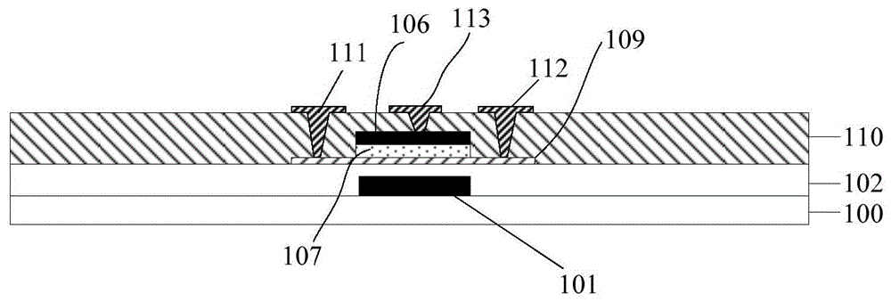
Fig. 1(a) to 1(g) are schematic flow charts of forming an oxide thin film transistor, and as shown in fig. 1(a) to 1(g), the method for manufacturing a display substrate according to the embodiment of the present disclosure includes the following steps:
step S1: as shown in fig. 1(a), a first gate electrode 101 of an oxide thin film transistor is formed on a substrate 100 through a patterning process.
In this step, the substrate 100 is a glass substrate, a quartz substrate, an organic substrate, or the like. Specifically, the first gate metal layer may be deposited by a sputtering method, a Plasma Enhanced Chemical Vapor Deposition (PECVD) method, a Low Pressure Chemical Vapor Deposition (LPCVD) method, an Atmospheric Pressure Chemical Vapor Deposition (APCVD) method, or an Electron Cyclotron Resonance Chemical Vapor Deposition (ECRCVD) method, and then the pattern 101 including the first gate of the oxide thin film transistor may be formed by a patterning process. Wherein the first gate metal layer includes: the composite material is a single-layer or multi-layer composite laminate formed by one or more of molybdenum (Mo), molybdenum-niobium alloy (MoNb), aluminum (Al), aluminum-neodymium alloy (AlNd), titanium (Ti) and copper (Cu), and is preferably a single-layer or multi-layer composite film formed by Mo, Al or Mo and Al-containing alloy. The process of patterning the gate metal layer using the mask to form the gate 101 is a conventional patterning process, and is not described herein again.
Step S2: as shown in fig. 1(b), a first gate insulating layer 102 is formed on a side of the first gate 101 facing away from the substrate 100. In this step, the first gate insulating layer 102 may be formed on the substrate 101 completed in step S1 by using a plasma enhanced chemical vapor deposition method, a low pressure chemical vapor deposition method, an atmospheric pressure chemical vapor deposition method, an electron cyclotron resonance chemical vapor deposition method, or a sputtering method.
The first gate insulating layer 102 may be silicon oxide (SiOx), silicon nitride (SiNx), hafnium oxide (HfOx), silicon oxynitride (SiON), aluminum oxide (AlOx), or a multilayer film including two or three of these. The material of the first gate insulating layer 102 in this embodiment is preferably silicon oxide.
Step S3: a first semiconductor material layer 103, a second gate insulating layer 104 and a second gate metal layer 105 are sequentially formed on the side, away from the substrate 100, of the first gate insulating layer 102, and a pattern 106 including an active layer 109 of an oxide thin film transistor, a pattern of a second gate insulating layer 107 and a second gate of the oxide thin film transistor is formed through a patterning process. The first semiconductor material layer of the present embodiment is an oxide semiconductor material layer.
In this step, first, the oxide semiconductor layer 103, the second gate insulating layer 104, and the second gate metal layer 105 are sequentially formed on the first gate insulating layer 102. The material of the oxide semiconductor layer 103 is any one of ITO (indium tin oxide), IZO (indium zinc oxide), IGZO (indium gallium zinc oxide), and InGaSnO (indium gallium tin oxide). The material of the oxide semiconductor layer 103 in this embodiment is preferably IGZO (indium gallium zinc oxide).
Then, a photoresist layer is coated on the second gate metal layer 105, and the photoresist layer is exposed by using a Half Tone Mask (HTM) or a Gray Tone Mask (GTM), and finally a pattern including the second gate 106 of the oxide thin film transistor, the second gate insulating layer 107, and the active layer 109 of the oxide thin film transistor is formed through the steps of developing, etching, and removing photoresist.
In some embodiments, step S3 specifically includes the following steps:
in step S31, the oxide semiconductor layer 103, the second gate insulating layer 104, and the second gate metal layer 105 are sequentially deposited on the side of the first gate insulating layer 101 away from the substrate 100.
In this step, as shown in fig. 1(c), first, the oxide semiconductor layer 103 is deposited on the first gate insulating layer 102 after step S2 by using a sputtering method, a thermal evaporation method, a plasma-enhanced chemical vapor deposition method, a low-pressure chemical vapor deposition method, an atmospheric pressure chemical vapor deposition method, or an electron cyclotron resonance chemical vapor deposition method.
Then, a second gate insulating layer 104 is deposited over the completed oxide semiconductor layer 103 by a plasma-enhanced chemical vapor deposition method, a low-pressure chemical vapor deposition method, an atmospheric pressure chemical vapor deposition method, an electron cyclotron resonance chemical vapor deposition method, or a sputtering method.
Further, a second gate metal layer 105 is deposited on the completed second gate insulating layer 104 by a sputtering method, a plasma enhanced chemical vapor deposition method, a low pressure chemical vapor deposition method, an atmospheric pressure chemical vapor deposition method, or an electron cyclotron resonance chemical vapor deposition method.
Step S32: a pattern including the second gate electrode 106 and the second gate insulating layer pattern 107 of the oxide thin film transistor is formed through a one-time patterning process.
In this step, as shown in fig. 1(d), a first photoresist is coated on the second gate metal layer 106 formed in step S32, and after the first photoresist is exposed and developed by using a half-tone mask (HTM) or a gray-tone mask (GTM), the second gate metal layer 105 and the second gate insulating layer 104 are sequentially etched to form a pattern including the second gate electrode 106 and the second gate insulating layer pattern 107 of the oxide thin film transistor.
Step S33: a second photoresist 108 is coated on a side of the second gate electrode 106 of the oxide thin film transistor facing away from the substrate, and a pattern including an active layer 109 of the oxide thin film transistor is formed through a one-time patterning process.
In this step, as shown in fig. 1(e) to 1(f), after patterning the second gate electrode 106 and the second gate insulating layer 107 including the oxide thin film transistor, a second photoresist 108 is coated on a side of the second gate electrode 106 of the oxide thin film transistor facing away from the substrate 100, and a pattern of the active layer 109 including the oxide thin film transistor is formed through exposure, development, etching, and photoresist removal steps. Wherein, the projection of the coated second photoresist 108 on the substrate 100 is completely overlapped with the projection of the channel region of the oxide thin film transistor active layer 109 on the substrate 100.
Step S4, forming a first interlayer insulating layer 110 on a side of the oxide thin film transistor where the second gate 106 is located away from the substrate 100, and forming a first source contact via, a first drain contact via, and a first connection via penetrating the first interlayer insulating layer 110, and a second connection via penetrating the first interlayer insulating layer 110, the first gate insulating layer 107, and the second gate insulating layer 102. A source electrode 111 and a drain electrode 112 of the oxide thin film transistor, and a gate line 113 are formed on a side of the first interlayer insulating layer 110 facing away from the substrate 100. The source 111 and the drain 112 of the oxide thin film transistor are electrically connected to the active layer 109 through a first source contact via and a first drain contact via, respectively; the gate line 113 is electrically connected to the second gate electrode 106 through the first connection via and to the first gate electrode 101 through the second connection via.
In this step, as shown in fig. 1(g) and fig. 2, first, the first interlayer insulator 110 may be deposited by a plasma enhanced chemical vapor deposition method, a low pressure chemical vapor deposition method, an atmospheric pressure chemical vapor deposition method, an electron cyclotron resonance chemical vapor deposition method, or a sputtering method. Then, a wet etching or dry etching process may be used to form a first source contact via, a first drain contact via, and a first connection via 114 penetrating the first interlayer insulating layer 110, and a second connection via 115 penetrating the first interlayer insulating layer 110, the first gate insulating layer 107, and the second gate insulating layer 102.
Then, a source-drain metal film may be deposited by a sputtering method, a thermal evaporation method, a plasma enhanced chemical vapor deposition method, a low pressure chemical vapor deposition method, an atmospheric pressure chemical vapor deposition method, or an electron cyclotron resonance chemical vapor deposition method, and a pattern including the source 111, the drain 112, and the gate line 113 of the oxide thin film transistor may be formed by a patterning process. In this embodiment, the gate line 113 and the source and drain electrodes 111 and 112 of the oxide thin film transistor are disposed at the same layer, the source and drain electrodes 111 and 112 of the oxide thin film transistor are electrically connected to the active layer 109 through the first source contact via and the first drain contact via, respectively, and the gate line 113 is electrically connected to the second gate electrode 106 through the first connection via 114 and electrically connected to the first gate electrode 101 through the second connection via 115.
The source-drain metal film can adopt a single-layer or multi-layer composite lamination formed by one or more of molybdenum (Mo), molybdenum-niobium alloy (MoNb), aluminum (Al), aluminum-neodymium alloy (AlNd), titanium (Ti) and copper (Cu); the preferable source-drain metal film adopts a composite lamination of molybdenum-niobium alloy and copper.
It should be noted that all the thin film transistors in the display substrate may be the same as the above-mentioned oxide thin film transistor preparation method, and are not described in detail here.
The oxide thin film transistor in this embodiment is a dual-gate oxide thin film transistor, and the oxide thin film transistor may be a top-gate oxide thin film transistor, a bottom-gate oxide thin film transistor, or the like, which is not particularly limited herein.
In this embodiment, the oxide semiconductor layer, the second gate insulating layer and the second gate metal layer are sequentially formed on the side, away from the substrate, of the first gate insulating layer of the oxide thin film transistor, and a pattern including the second gate, the second gate insulating layer pattern and the active layer of the oxide thin film transistor is formed through a patterning process.
In some embodiments, the display substrate may include a 2T1C pixel driving circuit, and the 2T1C pixel driving circuit includes a first thin film transistor and a second thin film transistor, which are illustrated in this embodiment as an oxide thin film transistor and a low temperature polysilicon thin film transistor. The oxide thin film transistor serves as a switching transistor, and the low temperature polysilicon thin film transistor serves as a driving transistor. It should be noted that the display substrate may further include a pixel driving circuit with other structures, such as a 7T2C structure, a 6T1C structure, an 8T2C structure, or a 9T2C structure, which is not limited in this disclosure.
It should be noted that the oxide thin film transistor in this embodiment is a dual-gate oxide thin film transistor, the low temperature polysilicon thin film transistor is a bottom gate type transistor, and the oxide thin film transistor and the low temperature polysilicon thin film transistor may also be other types of thin film transistors, which is not limited in this embodiment.
In this embodiment, the method for manufacturing a display substrate includes a step of forming a pixel driving circuit on a substrate, wherein the step of forming the pixel driving circuit includes a step of forming an oxide thin film transistor and a step of forming a low temperature polysilicon thin film transistor. Fig. 3 is a schematic structural diagram of a display substrate according to an embodiment of the present disclosure, where the step of forming an oxide thin film transistor on the display substrate and the step of forming a low temperature polysilicon thin film transistor specifically include:
step S400 of forming a pattern of the active layer 13 including the low temperature polysilicon thin film transistor on the substrate 1 through a patterning process.
And step S410, forming a third gate insulating layer 2 on one side of the active layer 13 of the low-temperature polycrystalline silicon thin film transistor, which is far away from the substrate 1.
In step S420, a gate 16 of the low temperature polysilicon thin film transistor is formed on a side of the third gate insulating layer 2 away from the substrate 1 by a patterning process.
And step S430, forming a second interlayer insulating layer 3 on the side of the grid 16 of the low-temperature polycrystalline silicon thin film transistor, which is far away from the substrate 1.
In step S440, a first gate electrode 6 of the oxide thin film transistor is formed on a side of the second interlayer insulating layer 3 away from the substrate 1 through a patterning process.
In step S440, a first gate insulating layer 4 is formed on a side of the first gate 6 facing away from the substrate 1.
And S450, sequentially forming an oxide semiconductor layer, a second grid insulating layer and a second grid metal layer on one side of the first grid insulating layer 4, which is far away from the substrate 1, and forming a pattern comprising an active layer 7 of an oxide thin film transistor, a second grid insulating layer 8 and a second grid 9 of the oxide thin film transistor through a composition process.
Step S460, forming a first interlayer insulating layer 5 on one side of the layer of the second grid 9 of the oxide thin film transistor, which is far away from the substrate 1, and forming a first source contact via hole, a first drain contact via hole, a second source contact via hole, a second drain contact via hole and a first connection via hole which penetrate through the first interlayer insulating layer 5, and a second connection via hole which penetrates through the first grid insulating layer, the first interlayer insulating layer and the second grid insulating layer.
Step S470, forming a source electrode 10 and a drain electrode 11 of an oxide thin film transistor, a source electrode 14 and a drain electrode 15 of a low temperature polysilicon thin film transistor and a grid line 12 on one side of the first interlayer insulating layer 5, which is far away from the substrate 1, through a patterning process; the source electrode 10 and the drain electrode 11 of the oxide thin film transistor are electrically connected with the active layer 7 of the oxide thin film transistor through a first source contact via hole and a first drain contact via hole, respectively; the source electrode 14 and the drain electrode 15 of the low-temperature polycrystalline silicon thin film transistor are electrically connected with the active layer 13 of the low-temperature polycrystalline silicon thin film transistor through a second source electrode contact through hole and a second drain electrode contact through hole respectively; the gate line 12 is electrically connected to the second gate electrode 9 through the first connection via and to the first gate electrode 6 through the second connection via.
In this embodiment, the forming process of the active layer, the gate electrode, the source electrode and the drain electrode of the low temperature polysilicon thin film transistor may be the same as or different from the forming process of the oxide thin film transistor, and is not limited herein. The formation method of the oxide thin film transistor is the same as the formation process of the oxide thin film transistor shown in fig. 1(a) to 1(f), and thus, detailed description thereof is omitted.
In this embodiment, the oxide semiconductor layer, the second gate insulating layer, and the second gate metal layer are sequentially formed on the side of the first gate insulating layer of the oxide thin film transistor away from the substrate, and a pattern including the second gate, the second gate insulating layer pattern, and the active layer of the oxide thin film transistor is formed by a patterning process. Furthermore, the source electrode and the drain electrode of the low-temperature polycrystalline silicon thin film transistor and the source electrode and the drain electrode of the oxide thin film transistor are formed by adopting a one-step composition process, so that the process steps are reduced, and the production cost is reduced.
The second aspect of the present embodiment also provides a display substrate, as shown in fig. 1(g) and fig. 2, the display substrate includes a substrate 100, and a first thin film transistor disposed on the substrate 100. The first gate 101 of the first thin film transistor is disposed on the substrate 100, and a first gate insulating layer 102 is disposed on a side of the first gate 101 of the first thin film transistor facing away from the substrate 100. The active layer 109 of the first thin film transistor is disposed on a side of the first gate insulating layer 102 facing away from the substrate 100. A second gate insulating layer 107 is provided on a side of the active layer 109 of the first thin film transistor facing away from the substrate 100. The second gate 106 of the first thin film transistor is disposed on a side of the first gate insulating layer 106 facing away from the substrate 100, and an orthographic projection of the second gate 107 of the first thin film transistor on the substrate is located within an orthographic projection of the active layer 109 of the first thin film transistor on the substrate 100. A first interlayer insulating layer 110 is disposed on a side of the second gate electrode 106 of the first thin film transistor facing away from the substrate 100. The source 111 and the drain 112 of the first thin film transistor, and the gate line 113 are located at a side of the first interlayer insulating layer 110 away from the substrate 100, and the source 111 and the drain 112 of the first thin film transistor are connected to the active layer 109 of the first thin film transistor through a source contact via and a drain contact via, respectively, which penetrate through the first interlayer insulating layer 110 and the second gate insulating layer 107, the gate line 113 is electrically connected to the second gate 106 of the first thin film transistor through a first connection via in the first interlayer insulating layer 110, and is electrically connected to the first gate 101 of the first thin film transistor through a second connection via in the first interlayer insulating layer 110, the second gate insulating layer 107, and the first gate insulating layer 102.
In this embodiment, the second gate electrode, the second gate insulating layer and the active layer of the first thin film transistor are sequentially formed on the side, away from the substrate, of the first gate insulating layer of the first thin film transistor, and the active layer of the first thin film transistor is formed after the second gate electrode and the second gate insulating layer of the first thin film transistor, so that the channel region of the active layer of the first thin film transistor is always in a protected state, the stability of the channel region of the active layer of the first thin film transistor is ensured, and the driving performance of the display substrate is further ensured.
In some embodiments, as shown in fig. 3, the display substrate further includes a pixel driving circuit disposed on the substrate 100, and the pixel driving circuit includes a first thin film transistor and a second thin film transistor. The source and drain electrodes 14 and 15 of the second thin film transistor are electrically connected to the active layer 13 of the second thin film transistor through second source and drain contact vias in the first interlayer insulating layer 5, respectively. The source electrode 14 and the drain electrode 15 of the second thin film transistor are arranged on the same layer as the source electrode 10 and the drain electrode 11 of the first thin film transistor, and are made of the same material.
In this embodiment, the second gate electrode, the second gate insulating layer and the active layer of the first thin film transistor are sequentially formed on the side, away from the substrate, of the first gate insulating layer of the first thin film transistor, and the active layer of the first thin film transistor is formed after the second gate electrode and the second gate insulating layer of the first thin film transistor, so that the channel region of the active layer of the first thin film transistor is always in a protected state, the stability of the channel region of the active layer of the first thin film transistor is ensured, and the driving performance of the display substrate is further ensured. Furthermore, the source electrode and the drain electrode of the second thin film transistor and the source electrode and the drain electrode of the first thin film transistor are formed by adopting a one-time composition process, so that the process steps are reduced, and the production cost is reduced.
In some embodiments, the material of the active layer of the first thin film transistor may include amorphous silicon, low temperature polysilicon, metal oxide, and the like. Preferably, the material of the active layer of the first thin film transistor of the present disclosure is a metal oxide, that is, the first thin film transistor is a metal oxide thin film transistor.
The third aspect of the present embodiment also provides a display device including the above display substrate. For example, in this embodiment, the display device may be a liquid crystal television, a notebook computer, a tablet computer, an electronic paper, or the like.
It is to be understood that the above embodiments are merely exemplary embodiments that are employed to illustrate the principles of the present disclosure, and that the present disclosure is not limited thereto. It will be apparent to those skilled in the art that various changes and modifications can be made therein without departing from the spirit and scope of the disclosure, and these are to be considered as the scope of the disclosure.