Detailed Description
Hereinafter, embodiments of the present invention will be described in detail with reference to the drawings. The embodiments and modifications described below are all general or specific examples. The numerical values, shapes, materials, constituent elements, arrangement of constituent elements, connection modes, and the like shown in the following examples and modifications are merely examples, and the gist thereof is not limited to the invention. Of the components of the following embodiments and modifications, components not described in the independent claims are described as arbitrary components. The sizes of the components shown in the drawings and the ratio of the sizes are not necessarily strict.
(embodiment mode)
[1 Circuit configuration of high-frequency Module and communication apparatus ]
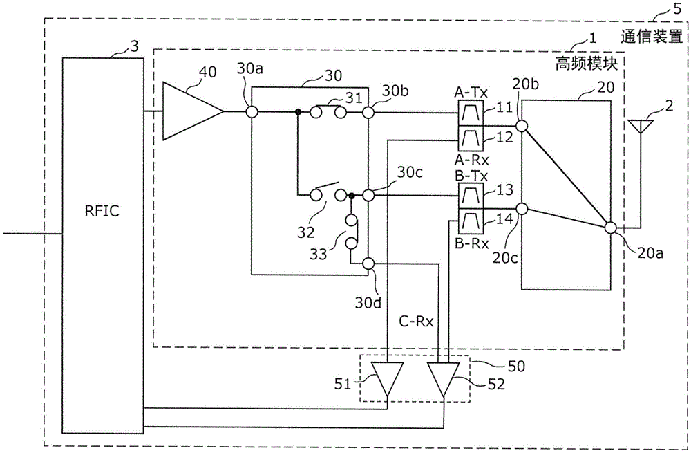
Fig. 1 is a circuit configuration diagram of a communication device 5 according to the embodiment. As shown in the drawing, the communication device 5 includes an antenna element 2, a high-Frequency module 1, a reception amplifier circuit 50, and an RF (Radio Frequency) signal processing circuit (RFIC) 3.
The RFIC 3 is an RF signal processing circuit that processes high-frequency signals transmitted and received by the antenna element 2. Specifically, the RFIC 3 performs signal processing on the high-frequency signal input through the reception path of the high-frequency module 1 by down-conversion or the like, and outputs the reception signal generated by the signal processing to a baseband signal processing circuit (not shown) or the like. The RFIC 3 performs signal processing on the transmission signal input from the baseband signal processing circuit by up-conversion or the like, and outputs a high-frequency signal generated by the signal processing to the transmission path of the high-frequency module 1.
The RFIC 3 also has a function as a control unit for controlling the connection of the switch circuits 20 and 30 included in the high-frequency module 1 based on the communication band (frequency band) used. Specifically, the RFIC 3 switches the connection of the switch circuits 20 and 30 included in the high-frequency module 1 by a control signal (not shown). The control unit may be provided outside the RFIC 3, for example, the high frequency module 1 or the baseband signal processing circuit.
The reception amplifier circuit 50 is composed of reception amplifiers 51 and 52. The reception amplifier 51 preferentially amplifies the reception signal of the band a (first communication band) among the reception signals output from the high frequency module 1, and outputs the amplified reception signal to the RFIC 3. The reception amplifier 52 preferentially amplifies the reception signals of the band B (second communication band) and the band C (third communication band) among the reception signals output from the high frequency module 1, and outputs the amplified reception signals to the RFIC 3.
The antenna element 2 is connected to the common terminal 20a of the switch circuit 20, radiates a high-frequency signal output from the high-frequency module 1, receives a high-frequency signal from the outside, and outputs the high-frequency signal to the high-frequency module 1.
In the communication device 5 according to the present embodiment, the antenna element 2 is not an essential component.
Next, the detailed structure of the high-frequency module 1 will be described.
As shown in fig. 1, the high-frequency module 1 includes transmission filters 11 and 13, reception filters 12 and 14, a transmission amplifier 40, and switch circuits 20 and 30.
The high-frequency module 1 according to the present embodiment is a high-frequency module capable of transmitting a transmission signal and a reception signal in a frequency band a (first communication frequency band), a transmission signal and a reception signal in a frequency band B (second communication frequency band), and a reception signal in a frequency band C (third communication frequency band). Also, the high frequency module 1 can perform: (1) CA that simultaneously performs transmission of a transmission signal of a frequency band a and a transmission signal of a frequency band B (2 uplink); (2) CA that simultaneously performs transmission of a transmission signal of a band a and reception of a reception signal of a band C (1 uplink 1 downlink); (3) CA that simultaneously performs reception of a reception signal of the band a and a reception signal of the band B (2 downlink); (4) CA for simultaneously performing reception of a reception signal of the frequency band a and a reception signal of the frequency band C (2 downlink); (5) CA that simultaneously performs transmission and reception of a transmission signal and a reception signal in a frequency band a and transmission and reception of a transmission signal and a reception signal in a frequency band B (2 uplink 2 downlink); (6) CA simultaneously performs transmission and reception of a transmission signal and a reception signal in the frequency band a and reception of a reception signal in the frequency band C (1 uplink 2 downlink).
Fig. 2 is a diagram illustrating an example of frequency allocation of communication bands that can be used by the high-frequency module 1 according to the embodiment. The Band a (first communication Band) in the present embodiment is, for example, band26 (transmission Band: 814MHz to 849MHz, reception Band: 859MHz to 894 MHz) of LTE (long term Evolution). The Band B (second communication Band) is, for example, band28 (transmission Band: 703MHz to 748MHz, reception Band: 758MHz to 803 MHz) of LTE. The frequency Band C (third communication Band) is, for example, band29 (reception Band: 717MHz-727 MHz) of LTE.
As illustrated in fig. 2, the Band a (Band 26) and the Band B (Band 28) have a transmission Band (Tx) and a reception Band (Rx), respectively. In addition, the Band C (Band 29) has only a reception Band (Rx). Here, the transmission Band of the Band B (Band 28) includes the reception Band of the Band C (Band 29).
The high-frequency module 1 according to the present embodiment includes a filter for passing the frequency bands a to C having the frequency relationship as described above, and a switch for switching the signal path of each communication frequency band.
The transmission filter 11 is a first transmission filter having a transmission band (a-Tx) of the frequency band a as a passband. The reception filter 12 is a first reception filter having a reception band (a-Rx) of the band a as a pass band.
The transmission filter 13 is a second transmission filter having a transmission band (B-Tx) of the band B as a passband. The reception filter 14 is a second reception filter having a reception band (B-Rx) of the band B as a pass band. The pass band of the transmission filter 13 includes a reception band (C-Rx) of the frequency band C.
The switch circuit 20 has a common terminal 20a (second common terminal), a selection terminal 20b (fifth selection terminal), and a selection terminal 20c (sixth selection terminal), and is a multi-connection type second switch circuit capable of simultaneously performing connection of the common terminal 20a and the selection terminal 20b and connection of the common terminal 20a and the selection terminal 20 c.
The selection terminal 20b is connected to the output terminal of the transmission filter 11 and the input terminal of the reception filter 12, and the selection terminal 20c is connected to the output terminal of the transmission filter 13 and the input terminal of the reception filter 14.
In the switch circuit 20, when at least one of transmission of a transmission signal of the band a and reception of a reception signal of the band a is performed, the common terminal 20a and the selection terminal 20b are brought into a conductive state. When at least one of transmission of a transmission signal of the band B, reception of a reception signal of the band B, and reception of a reception signal of the band C is performed, the common terminal 20a and the selection terminal 20C are brought into a conductive state. This makes it possible to make the output terminal of the transmission filter 11 and the output terminal of the transmission filter 13 unconnected when the CA is not present, and therefore the bandpass characteristic of the signal path selected when the CA is not present is improved.
The switch circuit 30 is a first switch circuit having a common terminal 30a (first common terminal), a selection terminal 30b (first selection terminal), a selection terminal 30c (second selection terminal), and a selection terminal 30d (third selection terminal), and switches 31, 32, and 33.
The switch 31 has one end connected to the common terminal 30a and the other end connected to the selection terminal 30b, and the switch 31 is a first switch for switching between conduction and non-conduction between the common terminal 30a and the selection terminal 30b. The switch 31 is, for example, a switching element of an SPST (Single Pole Single Throw) type.
The switch 32 has one end connected to the common terminal 30a and the other end connected to the selection terminal 30c, and the switch 32 is a second switch for switching between conduction and non-conduction between the common terminal 30a and the selection terminal 30 c. The switch 32 is, for example, an SPST type switching element.
The switch 33 has one end connected to the selection terminal 30c and the other end connected to the selection terminal 30d, and the switch 33 is a third switch for switching conduction and non-conduction between the selection terminal 30c and the selection terminal 30 d. The switch 33 is, for example, an SPST type switching element.
With the above configuration of the switch circuit 30, the switch circuit 30 is a multi-connection type switch circuit capable of simultaneously connecting 2 or more terminals among 4 terminals, i.e., the common terminal 30a and the selection terminals 30b, 30c, and 30 d.
The transmission amplifier 40 preferentially amplifies the transmission signals of the frequency bands a and B among the transmission signals output from the RFIC 3, and outputs the amplified transmission signals to the common terminal 30a of the switch circuit 30.
The common terminal 30a is connected to an output terminal of the transmission amplifier 40. The selection terminal 30b is connected to the input terminal of the transmission filter 11 and the output terminal of the reception filter 12. The selection terminal 30c is connected to the input terminal of the transmission filter 13 and the output terminal of the reception filter 14. The selection terminal 30d is connected to a reception path 61 through which a reception signal of the band C is transmitted, and is connected to the reception amplifier 52 via the reception path 61.
The selection terminal 20b is connected to the output terminal of the transmission filter 11 and the input terminal of the reception filter 12. The selection terminal 20c is connected to the output terminal of the transmission filter 13 and the input terminal of the reception filter 14. The input terminal of the reception amplifier 51 is connected to the output terminal of the reception filter 12. The input terminal of the reception amplifier 52 is connected to the output terminal of the reception filter 14.
In the high-frequency module 1 according to the present embodiment, the reception filters 12 and 14 and the switch circuit 20 are not essential components. In the communication device 5 according to the present embodiment, the antenna element 2 is not an essential component.
Fig. 3 is a circuit configuration diagram of a high-frequency module 500 according to a comparative example. The high-frequency module 500 shown in the figure is a conventionally conceived high-frequency module, and includes transmission filters 11 and 13, reception filters 12, 14, and 15, transmission amplifiers 41 and 42, and switch circuits 520 and 530. The high-frequency module 500 according to the present comparative example differs from the high-frequency module 1 according to the embodiment in the addition of the reception filter 15, the arrangement of 2 transmission amplifiers, and the configuration of the switch circuits 520 and 530. Next, the high-frequency module 500 according to the present comparative example will be described centering on differences from the high-frequency module 1 according to the embodiment, with descriptions of the same aspects as those of the high-frequency module according to the embodiment omitted.
The reception filter 15 is a filter having a reception band (C-Rx) of the frequency band C as a pass band.
The switch circuit 520 includes a common terminal 520a, selection terminals 520b, 520c, and 520d, and is a multi-connection type switch circuit capable of simultaneously performing at least 2 connections among the connection of the common terminal 520a to the selection terminal 520b, the connection of the common terminal 520a to the selection terminal 520c, and the connection of the common terminal 520a to the selection terminal 520 d.
The selection terminal 520b is connected to the output terminal of the transmission filter 11 and the input terminal of the reception filter 12, the selection terminal 520c is connected to the output terminal of the transmission filter 13 and the input terminal of the reception filter 14, and the selection terminal 520d is connected to the input terminal of the reception filter 15.
The switch circuit 530 is a switch circuit having terminals 530a, 530b, 530c, and 530d and switches 531 and 532. The switch 531 has one end connected to the terminal 530a and the other end connected to the terminal 530c, and the switch 531 switches conduction and non-conduction between the terminal 530a and the terminal 530 c. The switch 532 has one end connected to the terminal 530b and the other end connected to the terminal 530d, and the switch 532 switches conduction and non-conduction between the terminal 530b and the terminal 530 d.
With the above-described configuration of the switch circuit 530, the switch circuit 530 is a multi-connection type switch circuit capable of simultaneously performing connection between the terminal 530a and the terminal 530c and connection between the terminal 530b and the terminal 530 d.
The transmission amplifier 41 preferentially amplifies the high-frequency signals of the band a among the high-frequency signals output from the RFIC 3, and outputs the amplified transmission signals to the terminal 530a. The transmission amplifier 42 preferentially amplifies the high-frequency signal of the band B among the high-frequency signals output from the RFIC 3, and outputs the amplified transmission signal to the terminal 530B.
The terminal 530a is connected to the output terminal of the transmission amplifier 41. The terminal 530b is connected to the output terminal of the transmission amplifier 42. Terminal 530c is connected to an input terminal of transmission filter 11. The terminal 530d is connected to an input terminal of the transmission filter 13.
According to the above-described configuration of the high-frequency module 500 according to the comparative example, the transmission signal and the reception signal in the frequency band a, the transmission signal and the reception signal in the frequency band B, and the reception signal in the frequency band C can be transmitted. Further, the high frequency module 500 can perform (1) CA for simultaneously transmitting a transmission signal in the frequency band a and a transmission signal in the frequency band B (2 uplink), and (5) CA for simultaneously transmitting and receiving a transmission signal in the frequency band a and a transmission signal in the frequency band B (2 uplink 2 downlink), by turning the switches 531 and 532 into the on state, connecting the common terminal 520a to the selection terminal 520B, and connecting the common terminal 520a to the selection terminal 520 c. Further, by turning on the switch 531, connecting the common terminal 520a to the selection terminal 520b, and connecting the common terminal 520a to the selection terminal 520d, (2) CA for simultaneously transmitting a transmission signal in the frequency band a and receiving a reception signal in the frequency band C (1 uplink 1 downlink), and (6) CA for simultaneously transmitting and receiving a transmission signal in the frequency band a and a reception signal in the frequency band C (1 uplink 2 downlink) can be performed. Further, by connecting the common terminal 520a to the selection terminal 520B and connecting the common terminal 520a to the selection terminal 520c, (3) CA for simultaneously receiving the reception signal of the frequency band a and the reception signal of the frequency band B (2 downlink) can be performed. Further, by connecting the common terminal 520a to the selection terminal 520b and connecting the common terminal 520a to the selection terminal 520d, (4) CA for simultaneously receiving the reception signal of the frequency band a and the reception signal of the frequency band C (2 downlink) can be performed.
However, in the high-frequency module 500 according to the comparative example, 2 transmission amplifiers are arranged corresponding to the bands a and B, respectively, and the reception filter 15 dedicated to the reception band of the band C is arranged, so that the high-frequency module 500 is large in size.
On the other hand, since the reception band (C-Rx) of the band C is in a relationship of the transmission band (B-Tx) included in the band B, the following is conceivable: the transmission filter of the band B is also applied as the reception filter of the band C as a countermeasure for miniaturization. In addition, if a transmission amplifier capable of amplifying high-frequency signals of the band a and the band B is used, the number of transmission amplifiers can be reduced as compared with the high-frequency module 500 according to the comparative example, and thus the high-frequency module can be further miniaturized.
In the case where the transmission filter of the band B is also applied as the reception filter of the band C, since the reception filter of the band C is a filter that passes the reception signal, in the case where the transmission filter of the band B is used as the reception filter of the band C, it is necessary to connect the transmission filter of the band B and the reception amplification circuit by a switch circuit.
In addition, when a transmission amplifier capable of amplifying high-frequency signals in the band a and the band B is disposed, both the transmission filter in the band a and the transmission filter in the band B need to be connected to the transmission amplifier.
Here, when the transmission of the transmission signal of the band a and the reception of the reception signal of the band C are performed simultaneously, it is necessary to connect the transmission amplifier to the transmission filter of the band a and connect the transmission filter of the band B to the reception path of the reception signal of the transmission band C via the switch circuit. However, when both the transmission filter of the band a and the transmission filter of the band B are connected to the transmission amplifier and the transmission filter of the band B is connected to the reception path of the band C, there is a problem as follows: the transmission signal from the transmission amplifier leaks to the reception path via the switch circuit, and the reception sensitivity in the reception path is lowered.
In contrast, according to the above configuration of the high-frequency module 1 according to the present embodiment, since the switch 32 is disposed between the common terminal 30a and the selection terminal 30C, and the switch 33 is disposed between the selection terminal 30C and the selection terminal 30d, when the transmission of the transmission signal in the band a and the reception of the reception signal in the band C are simultaneously performed, by making the switch 32 non-conductive and making the switch 33 conductive, it is possible to improve the isolation between the transmission signal in the band a and the reception signal in the band C while using the transmission filter 13 as a filter through which the reception signal in the band C passes. When the transmission signal of the band a and the transmission signal of the band B are not simultaneously transmitted, the isolation between the transmission signal of the band a and the transmission signal of the band B can be ensured by the switching operation of the switches 31 and 32 even if 1 transmission amplifier 40 is shared by the transmission amplifiers that amplify the high frequency signals of the band a and the band B. Therefore, the high-frequency module 1 and the communication device 5, which include the reception band of the frequency band C in the transmission band of the frequency band B and simultaneously perform transmission of the transmission signal of the frequency band a and reception of the reception signal of the frequency band C, can be downsized, and a decrease in the reception sensitivity in the frequency band C can be suppressed. That is, it is possible to provide a high-frequency module and a communication apparatus capable of performing CA in a plurality of communication bands including 2 communication bands in which a transmission band of one communication band and a reception band of another communication band are in an inclusive relationship, and suppressing a decrease in reception sensitivity while being miniaturized.
In addition, the switch Circuit 30 may be formed in 1 switch IC (Integrated Circuit). When the switch circuit 30 is formed in 1 switch IC, the space between the common terminal 30a and the selection terminals 30b to 30d is reduced, and therefore, the isolation of the high-frequency signal between the communication bands is deteriorated. In contrast, according to the above configuration of the switch circuit 30, the isolation between the transmission signal of the band a and the reception signal of the band C can be improved by making the switch 32 non-conductive. Therefore, the reception sensitivity in the band C can be improved while miniaturizing the high-frequency module 1.
The switching circuits 20 and 30 and the control unit may constitute 1 switching IC. This can shorten the control wiring connecting the control unit and the switch circuits 20 and 30, and thus can suppress the control signal from interfering with the high-frequency signal, thereby reducing the control accuracy. Further, the high-frequency module 1 can be manufactured at low cost by configuring the switch IC with a Si-based CMOS (Complementary Metal Oxide Semiconductor).
[2 Circuit operation of high-frequency Module ]
Fig. 4A is a diagram showing a circuit state in the case where CA of the band a and the band B is performed in the high-frequency module 1 according to embodiment 1. The circuit state in the case of CA for transmission and reception signals in band a and transmission and reception signals in band B is shown in the figure.
When transmission and reception of the transmission signal and the reception signal in the frequency band a and transmission and reception of the transmission signal and the reception signal in the frequency band B are performed simultaneously, the switches 31 and 32 are turned on, and the switch 33 is turned off. The common terminal 20a and the selection terminal 20b are connected, and the common terminal 20a and the selection terminal 20c are connected.
Thereby, the transmission signal of the band a is transmitted to the antenna element 2 via the transmission amplifier 40, the common terminal 30a, the switch 31, the selection terminal 30b, the transmission filter 11, the selection terminal 20b, and the common terminal 20 a. The transmission signal of the band B is transmitted to the antenna element 2 via the transmission amplifier 40, the common terminal 30a, the switch 32, the selection terminal 30c, the transmission filter 13, the selection terminal 20c, and the common terminal 20 a.
Here, since the switch 33 is in the non-conductive state, leakage of the transmission signal in the frequency band a and the transmission signal in the frequency band B to the reception path in the frequency band C can be suppressed, and therefore the transmission signal in the frequency band a and the transmission signal in the frequency band B can be transmitted to the antenna element 2 with low loss.
In addition, the reception signal of the band a is transmitted to the RFIC 3 via the antenna element 2, the common terminal 20a, the selection terminal 20b, the reception filter 12, and the reception amplifier 51. In addition, the reception signal of the band B is transmitted to the RFIC 3 via the antenna element 2, the common terminal 20a, the selection terminal 20c, the reception filter 14, and the reception amplifier 52.
Fig. 4B is a diagram showing a circuit state in a case where CA of the frequency band a and the frequency band C is executed in the high-frequency module 1 according to embodiment 1. The circuit state in the case of CA for the transmission signal and the reception signal in the frequency band a and the reception signal in the frequency band C is shown in the figure.
When the transmission signal and the reception signal of the frequency band a are transmitted and received simultaneously with the reception signal of the frequency band C, the switches 31 and 33 are turned on, and the switch 32 is turned off. The common terminal 20a and the selection terminal 20b are connected, and the common terminal 20a and the selection terminal 20c are connected.
Thereby, the transmission signal of the band a is transmitted to the antenna element 2 via the transmission amplifier 40, the common terminal 30a, the switch 31, the selection terminal 30b, the transmission filter 11, the selection terminal 20b, and the common terminal 20 a.
Here, since the switch 32 is in a non-conductive state, leakage of the transmission signal output from the transmission amplifier 40 to the transmission path of the band B and the reception path of the band C can be suppressed. Therefore, the following can be suppressed: the high-frequency component of the band B (and the band C) transmitted through the transmission path of the band B is coupled to the transmission signal of the band a transmitted through the transmission path of the band a and output to the antenna element 2 in the switch circuit 20. In addition, the transmission signal output from the transmission amplifier 40 can be suppressed from flowing into the reception path of the band C.
In addition, the reception signal of the band a is transmitted to the RFIC 3 via the antenna element 2, the common terminal 20a, the selection terminal 20b, the reception filter 12, and the reception amplifier 51. The reception signal of the band C is transmitted to the RFIC 3 via the antenna element 2, the common terminal 20a, the selection terminal 20C, the transmission filter 13, the selection terminal 30C, the switch 33, the selection terminal 30d, and the reception amplifier 52.
As shown in fig. 4A and 4B, CA (2 uplink 2 downlink) of the transmission signal and the reception signal in the band a and the transmission signal and the reception signal in the band B and CA (1 uplink 2 downlink) of the transmission signal and the reception signal in the band a and the reception signal in the band C can be switched by the above-described connection state of the switch circuits 20 and 30.
Note that, although not shown, when the transmission signal of the band a and the transmission signal of the band B are simultaneously transmitted, the switches 31 and 32 are in a conductive state, and the switch 33 is in a non-conductive state. When the transmission signal of the band a and the reception signal of the band C are simultaneously transmitted, the switches 31 and 33 are turned on, and the switch 32 is turned off. In either case, the common terminal 20a and the selection terminal 20b are connected, and the common terminal 20a and the selection terminal 20c are connected.
Thus, CA (1 uplink 1 downlink) of the transmission signal of the band a and the reception signal of the band C and CA (2 uplink) of the transmission signal of the band a and the transmission signal of the band B can be switched by the switch circuits 20 and 30.
Although not shown, when the reception signal of the band a and the reception signal of the band B are simultaneously received, the switch 33 is in a non-conductive state. When the reception signal of the band a and the reception signal of the band C are simultaneously received, the switch 33 is turned on. In either case, the common terminal 20a and the selection terminal 20b are connected, and the common terminal 20a and the selection terminal 20c are connected.
Thus, CA (2 downlink) of the received signal of the band a and the received signal of the band B and CA (2 downlink) of the received signal of the band a and the received signal of the band C can be switched by the switch circuits 20 and 30.
[3 high-frequency Module according to modification 1 ]
Fig. 5 is a circuit configuration diagram of a high-frequency module 1A according to modification 1 of the embodiment. As shown in the figure, the high-frequency module 1A includes transmission filters 11 and 13, reception filters 12 and 14, a transmission amplifier 40, and switch circuits 20 and 60. The high-frequency module 1A according to the present modification differs from the high-frequency module 1 according to the embodiment only in the configuration of the switch circuit 60. Next, the high-frequency module 1A according to the present modification will be described centering on differences from the high-frequency module 1 according to the embodiment, with the description of the same aspects as those of the high-frequency module 1 according to the embodiment omitted.
The switch circuit 60 is a first switch circuit having a common terminal 30a (first common terminal), a selection terminal 30b (first selection terminal), a selection terminal 30c (second selection terminal), and a selection terminal 30d (third selection terminal), and switches 31, 32, 33, and 34.
The switch 31 has one end connected to the common terminal 30a and the other end connected to the selection terminal 30b, and the switch 31 is a first switch for switching between conduction and non-conduction between the common terminal 30a and the selection terminal 30b. The switch 31 is, for example, an SPST type switching element.
The switch 32 has one end connected to the switch 34 and the other end connected to the selection terminal 30c, and the switch 32 is a part of a second switch that switches conduction and non-conduction between the common terminal 30a and the selection terminal 30 c. The switch 32 is, for example, an SPST type switching element.
The switch 34 has one end connected to the common terminal 30a and the other end connected to the switch 32, and the switch 34 is a part of a second switch that switches conduction and non-conduction between the common terminal 30a and the selection terminal 30 c. The switch 34 is, for example, an SPST type switching element.
The switches 32 and 34 are 2 switching elements connected in series with each other, and constitute a second switch for switching conduction and non-conduction between the common terminal 30a and the selection terminal 30 c. In the high-frequency module 1A according to modification 1, the switches connected in series between the common terminal 30a and the selection terminal 30c are not limited to 2 switching elements as in the case of the switches 32 and 34, and may be 2 or more switching elements connected in series.
The switch 33 has one end connected to the selection terminal 30c and the other end connected to the selection terminal 30d, and the switch 33 is a third switch for switching conduction and non-conduction between the selection terminal 30c and the selection terminal 30 d. The switch 33 is, for example, an SPST type switching element.
With the above configuration of the switch circuit 60, the switch circuit 60 is a multi-connection type switch circuit capable of simultaneously connecting 2 or more terminals among 4 terminals, i.e., the common terminal 30a and the selection terminals 30b, 30c, and 30 d.
The switches 32 and 34 are simultaneously turned on or simultaneously turned off. That is, the switches 32 and 34 function as 1 second switch.
According to the above configuration, the second switch is arranged between the common terminal 30a and the selection terminal 30c, and the second switch is constituted by 2 switches 32 and 34 connected in series. Thus, when the second switch is set to the non-conductive state, leakage of the high-frequency signal output from the transmission amplifier 40 to the transmission path of the band B and the reception path of the band C can be further suppressed. Therefore, the isolation between the transmission signal in the band a and the reception signal in the band C can be further improved. Therefore, the reception sensitivity in the band C can be further improved while the high-frequency module 1A is miniaturized.
Fig. 6 is a graph comparing the bandpass characteristics of the high-frequency module according to the embodiment and the high-frequency module according to modification 1. The figure shows the bandpass characteristics from the common terminal 30a to the common terminal 20a including the transmission filter 11 in the high-frequency module 1 according to the embodiment and the high-frequency module 1A according to the modification 1. Further, the switch 31 is in a conductive state, the switches 32 and 34 are in a non-conductive state, and the common terminal 20a and the selection terminal 20b are connected. Note that LTE Band26 is applied to Band a, LTE Band28 is applied to Band B, and LTE Band29 is applied to Band C.
In the high-frequency module according to the embodiment and the modification 1, there is no difference in the insertion loss in the transmission band (B26-Tx) of the band a. In contrast, the high-frequency module 1A according to modification 1 is more optimized than the high-frequency module 1 according to the embodiment in the attenuation characteristics in the band C (B29-Rx). While the attenuation in the frequency band C (B29-Rx) is about 25dB in the high-frequency module 1 according to the embodiment, the attenuation in the frequency band C (B29-Rx) is about 38dB in the high-frequency module 1A according to the modification 1.
When the transmission signal of the band a and the reception signal of the band C are simultaneously transmitted, the switches 31 and 33 are turned on, and the switch 32 (second switch) is turned off. In this case, the transmission signal output from the transmission amplifier 40 passes through the transmission path of the band a and the transmission filter 11 via the on-state switch 31, and is output to the antenna element 2. At this time, a part of the transmission signal output from the transmission amplifier 40 flows into the transmission path of the band B and the reception path of the band C via the switch 32 (second switch) in the non-conductive state, and the unnecessary wave having the frequency component of the band B (and the band C) flows into the transmission path of the band a in the switch circuit 20 and the like. That is, in the band-pass characteristics from the common terminal 30a to the common terminal 20a including the transmission filter 11, the attenuation characteristics in the band B (and the band C) are affected by the isolation performance at the time of non-conduction of the switch 32.
According to the high-frequency module 1A of modification 1, the second switch for switching the connection between the common terminal 30a and the selection terminal 30c is constituted by the 2 switches 32 and 34 connected in series, and the isolation performance of the second switch in the non-conduction state is improved. This can suppress the following: the transmission signal output from the transmission amplifier 40 flows into the transmission path of the band B and the reception path of the band C via the second switch in the non-conductive state.
Therefore, when the transmission signal of the band a and the reception signal of the band C are simultaneously transmitted, the isolation between the transmission signal of the band a and the reception signal of the band C can be further improved. Therefore, the reception sensitivity in the band C can be further improved while the high-frequency module 1A is miniaturized.
[4 high-frequency Module according to variation 2 ]
Fig. 7 is a circuit configuration diagram of a high-frequency module 1B according to modification 2 of the embodiment. As shown in the figure, the high-frequency module 1B includes transmission filters 11 and 13, reception filters 12 and 14, a transmission amplifier 40, switching circuits 20 and 70, and an inductor 80. The high-frequency module 1B according to the present modification differs from the high-frequency module 1A according to modification 1 in the configuration of the switching circuit 70 and the addition of the inductor 80. Next, the high-frequency module 1B according to the present modification is not described in the same manner as the high-frequency module 1A according to the modification 1, and a description thereof will be given centering on a different aspect.
The switch circuit 70 is a first switch circuit having a common terminal 70a (first common terminal), a selection terminal 70b (first selection terminal), a selection terminal 70c (second selection terminal), a selection terminal 70d (third selection terminal), and a selection terminal 70e (fourth selection terminal), and switches 71, 72, 73, 74, and 75.
The switch 71 has one end connected to the common terminal 70a and the other end connected to the selection terminal 70b, and the switch 71 is a first switch for switching between conduction and non-conduction between the common terminal 70a and the selection terminal 70 b. The switch 71 is, for example, an SPST type switching element.
The switch 72 has one end connected to the switch 74 and the other end connected to the selection terminal 70c, and the switch 72 is a part of a second switch that switches conduction and non-conduction between the common terminal 70a and the selection terminal 70 c. The switch 72 is, for example, an SPST type switching element.
The switch 74 has one end connected to the common terminal 70a and the other end connected to the switch 72, and the switch 74 is a part of a second switch that switches conduction and non-conduction between the common terminal 70a and the selection terminal 70 c. The switch 74 is, for example, an SPST type switching element.
The switch 73 has one end connected to the selection terminal 70c and the other end connected to the selection terminal 70d, and the switch 73 is a third switch for switching conduction and non-conduction between the selection terminal 70c and the selection terminal 70 d. The switch 73 is, for example, an SPST type switching element.
One end of the switch 75 is connected to a connection point of the switches 72 and 74, and the other end is connected to the selection terminal 70e, and the switch 75 is a fourth switch that switches conduction and non-conduction between the connection point and the selection terminal 70e. The switch 75 is, for example, an SPST type switching element. One end of the switch 75 may not be connected to the connection point, and may be connected to the common terminal 70a or the selection terminal 70 c.
The inductor 80 has one end connected to the selection terminal 70e and the other end connected to ground. The other end of the inductor 80 may not be connected to ground.
When the transmission signal of the band a and the reception signal of the band C are simultaneously transmitted, the switches 71 and 73 are turned on, and the switches 72 and 74 are turned off. In this case, the transmission signal output from the transmission amplifier 40 passes through the transmission path of the band a and the transmission filter 11 via the on-state switch 71, and is output to the antenna element 2. At this time, part of the transmission signal output from the transmission amplifier 40 flows into the transmission path of the band B and the reception path of the band C via the switches 72 and 74 in the non-conductive state, and the unnecessary wave having the frequency component of the band B (and the band C) flows into the reception path of the band C, thereby lowering the reception sensitivity in the band C.
In contrast, in the high-frequency module 1B according to the present modification, the off-capacitances of the switches 72 and 74 and the inductor 80 constitute a filter on a path connecting the common terminal 70a and the selection terminal 70 c. Here, the inductance value of the inductor 80 can be adjusted to provide the filter with a band pass characteristic having the band C as an attenuation band.
Thus, when CA of the transmission signal of the band a and the reception signal of the band C is executed, the switches 71 and 73 are brought into the conductive state, the switches 72 and 74 are brought into the non-conductive state, and the switch 75 is brought into the conductive state, whereby the unnecessary signal of the frequency component of the band C, which is leaked to the selection terminal 70C after the switches 72 and 74 in the non-conductive state, can be attenuated by the filter constituted by the inductor 80 and the switches 72 and 74. Therefore, the reception sensitivity in the band C can be further improved.
Further, the circuit element connected to the selection terminal 70e is not limited to the inductor 80. The method can be as follows: on a path connecting the common terminal 70a and the selection terminal 70C, a circuit element necessary for having a filter function for attenuating an unnecessary signal in the frequency band of the band C is connected to the selection terminal 70e. The required circuit element is, for example, at least one of an inductor and a capacitor.
(other embodiments)
The high-frequency module and the communication device according to the present invention have been described above by referring to the embodiments and the modifications, but the present invention is not limited to the embodiments and the modifications. Other embodiments in which arbitrary components in the above-described embodiment and modifications are combined, modifications in which various modifications that can be made to the above-described embodiments by those skilled in the art are made without departing from the spirit and scope of the present invention, and various devices incorporating the high-frequency module and the communication device according to the present invention are also included in the present invention.
For example, in the high-frequency module and the communication device according to the embodiments and the modifications, matching elements such as inductors and capacitors, and switching circuits may be connected between the respective components. The inductor may include a wiring inductance formed by a wiring connecting the components.
Industrial applicability
The present invention is widely applicable to communication devices such as mobile phones as a high-frequency module and a communication apparatus applicable to a multiband system that executes CA.
Description of the reference numerals
1. 1A, 1B, 500: a high frequency module; 2: an antenna element; 3: RF signal processing circuitry (RFIC); 5: a communication device; 11. 13: a transmission filter; 12. 14, 15: a receiving filter; 20. 30, 60, 70, 520, 530: a switching circuit; 20a, 30a, 70a, 520a: a common terminal; 20b, 20c, 30b, 30c, 30d, 70b, 70c, 70d, 70e, 520b, 520c, 520d: a selection terminal; 31. 32, 33, 34, 71, 72, 73, 74, 75, 531, 532: a switch; 40. 41, 42: a transmission amplifier; 50: a receiving amplifying circuit; 51. 52: a receiving amplifier; 80: an inductor; 530a, 530b, 530c, 530d: and a terminal.