Background
At present, a triple-modular redundancy fault-tolerant computer used in the prior art has a more urgent application requirement in the field of safety key control because of higher safety performance. In the field of aerospace, a digital time division command response type multi-channel transmission data bus (MIL-STD-1553B bus, 1553B for short) is a widely used electronic system field bus and has the characteristics of excellent reliability, high transmission rate and high anti-interference capability.
1553B bus terminal types there are three types of existing bus controllers, remote terminals and bus monitors. As shown in the attached fig. 1, in a 1553B Bus Controller (BC) interface of a triple-modular redundancy computer, three machines share a 1553B bus communication chip configured in a BC mode. In the mode, the data sources of the three machines are all the same bus chip, so that a single point exists in the system. When the chip fails, the communication of the three devices is abnormal, the single-point fault cannot be shielded through a voting mechanism, and even if the design of redundant backup of the 1553B bus communication chip is adopted, certain system recovery time is required for detecting the fault and recovering the bus communication, so that task interruption is caused.
As shown in the attached fig. 2, in a Bus Controller (BC) interface of the triple-modular redundancy computer 1553B, each single machine has an independent bus communication chip and is configured in a BC mode, wherein only the bus chip of one machine (generally, a host) is accessed to a bus communication network as an active BC, and the other two machine bus chips are not accessed, that is, the active BC is not accessed; the bus data of the inactive BC computer is transmitted for the active BC computer through the three-computer communication channel. Therefore, the data of the three machines only enter the three-machine system from one bus chip interface at the same time and are definitely completely the same, and the voting mechanism cannot play a role; moreover, the three machines are inconsistent in operation flow, and when a failover activity BC is detected, the system needs a certain recovery time, which causes task discontinuity.
As shown in the attached fig. 3, each single unit in the interface of the Bus Controller (BC) of the triple-modular redundant computer 1553B has a separate bus chip, one of the units is configured in a BC mode (generally, a host) of the bus controller, the other two units are configured in a bus Monitor (MT) mode, and data of the three units are sourced from different bus channels. Because the bus chips of the three machines work in different modes, the bus data of the three machines are not completely consistent and need to be processed. Meanwhile, because the three-machine bus chip works in different modes, the running flows of the three machines are different, and the system needs a certain recovery time after the fault degradation, thereby being incapable of realizing the uninterrupted work of the bus communication interface.
As for the three interface modes applied in the prior art, when the control system is out of service for a long time, serious consequences (for example, when a rocket is launched and lifted, the whole launching task will fail if the control bus communication system is interrupted, and when an airplane flies, the airplane cannot fly normally and the flight safety is seriously affected if the control bus communication system is interrupted), the existing bus redundancy synchronous communication system cannot be applied, and a bus redundancy synchronous communication system is urgently needed to realize redundancy and uninterrupted work.
In view of this, the present patent application is specifically proposed.
Disclosure of Invention
The redundancy synchronous communication method of the multi-channel transmission data bus aims to solve the problems in the prior art, provides a 1553B bus controller interface redundancy method for a multi-mode redundancy computer, aims to solve the problems that the interface of the 1553B bus controller of the existing multi-mode redundancy fault-tolerant computer is single-point and the working state recovery time is too long during reconstruction recovery, and can expand a multi-machine type redundancy fault-tolerant system.
In order to achieve the design purpose, the redundancy synchronous communication method of the multi-channel transmission data bus adopts a multi-mode mutual redundancy bus interface mode, a single machine where each CPU is located is provided with an independent bus communication chip, working modes of 1553B buses are configured into a BC mode and are accessed into a bus communication network; the communication mechanism comprises that only one terminal controls the bus system at any time, namely only one active BC is arranged on the bus at any time; the minimum unit of the 1553B communication sequence is a message, an instruction word in the message is transmitted by BC, a state word is transmitted by RT, and the message transmission sequence determines that the BC is not transmitted and does not receive RT feedback; the interval time of the RT response effective instruction word is 4-12us, the minimum no response timeout is 14us, and 2us after the BC sends the word, the RT response is detected.
Specifically, host switching can be realized by rewriting program instructions of the FPGA, and the interaction between the CPU and the FPGA realizes an instruction primitive for controlling the CPU to wait.
Further, the process of sending data by the 1553B bus is as follows:
data exchange is carried out on data to be sent through a three-machine data exchange interface;
voting by two out of three after data exchange to obtain voted data;
the voted data is filled into a sending data 1553B message frame;
filling the combined 1553B message frame into a bus chip to prepare for starting bus communication;
the method needs to start bus communication and comprises the following steps: 1. closing the interrupt; 2. synchronizing the three machines; 3. starting 1553B bus communication; 4. starting an interrupt;
after waiting for 1553B bus communication interrupt return, reading out a state word of bus communication in the interrupt processing to obtain a data transmission result;
and carrying out corresponding processing according to the sending result.
Based on the same design concept, the process of receiving data by the 1553B bus is as follows:
framing the acquired remote terminal data message, and writing the framed remote terminal data message into a 1553B bus chip;
starting bus communication, wherein the starting step is divided into the following steps: 1. closing the interrupt; 2. synchronizing the three machines; 3. starting 1553B bus communication; 4. starting an interrupt;
after the 1553B bus communication interrupt returns, the bus communication data is read out in the interrupt processing, and the remote terminal data is obtained;
carrying out data exchange on received data;
voting the received data of the three-machine by two out of three after exchanging to obtain the received data after voting;
and correspondingly processing the received data.
In summary, the multiplexing data bus redundancy synchronous communication method has the advantages that the 1553B-based bus controller interface can completely eliminate single-point failures of the interface, and actively performs failure switching when a host computer failure is detected without interrupting the current task; in the switching process, the recovery work of the interface is not needed, so that seamless switching is really realized to ensure the continuous working state of the system, the reliability and the safety of the system are improved, and the method can adapt to the working environment with more severe task continuity.
Detailed Description
The following further describes embodiments of the present invention with reference to the drawings.
In embodiment 1, the multiplexing data bus redundancy synchronous communication method described in this application adopts a bus interface mode as shown in fig. 4, that is, a triple-modular redundancy computer has three CPUs (i.e., three mutually redundant computer modules), where only one master right is provided, and the other slave is default at the initial power-on. When the current chip is detected to be in fault, the host can be randomly selected from the 3 computer modules at any time.
Specifically, host switching is achieved by rewriting program instructions of the FPGA.
The single machine where each CPU is located is provided with an independent bus communication chip, and 1553B bus working modes are all configured into a BC mode and are all accessed to a bus communication network.
Using the above bus interface mode, the present application mainly adopts the following 3 solutions: 1. only one terminal is required to control the bus system at any time, namely only one active BC is available on the bus at any time; 2. the minimum unit of the 1553B communication sequence is a message, an instruction word in the message is transmitted by BC, a state word is transmitted by RT, and the message transmission sequence determines that the BC is not transmitted and does not receive RT feedback; 3. the interval time of the RT response effective instruction word is 4-12us, the minimum no response timeout is 14us, and 2us after the BC sends the word, the RT response is detected.
For the implementation of the above mechanism, as shown in fig. 5, for the mechanism 1, the bus chip is configured to have an output enable control function, and the enable signal is changed along with the exchange of the master rights among the three devices. If and only if, only the output of the host bus is enabled, the output of the other two buses is disabled (the chip normally outputs signals, the input and output logic function of the chip is normally executed, but the output signals are not accessed into the bus, only the signals output by the host chip are on the bus, and only one bus controller controls the bus system at any moment); meanwhile, when the bus chip outputs the forbidden state, the chip can normally send data, but the sent data cannot be accessed into the bus network, and the chip can normally receive the bus network data.
For the mechanism 2, in the process of sending and receiving data on the 1553B bus, because the minimum unit of the 1553B communication sequence is a message, and the message transmission sequence determines that BC is not sent, RT feedback cannot be received, so that in the process of sending/receiving data on the 1553B bus, regardless of whether a computer module is a host, a 1553B communication bus chip executes a motion of 'starting 1553B bus communication'. The bus chip of the slave machine is forbidden due to the bus output, the BC sending word can not be actually sent, but the RT feedback word can be received, and a 1553B communication sequence can also be ensured on the slave machine. Therefore, all CPU modules of the computer execute the same flow, and the time for recovering the working state is not needed when the running state of the three computers is synchronous, the redundancy synchronization of the bus interface and the switching of the control right of the bus, thereby realizing the uninterrupted work of the bus communication interface.
For the mechanism 3, based on the mechanisms 1 and 2, as shown in the bus message sequence generation shown in fig. 5, if the slave wants to send an RT return word obtained by a word as its response by the master BC, there are two ways: firstly, the slave is faster than the master (such as the slave 1 in fig. 5), the interval time of the RT response valid command word is 4us-12us, and the minimum no-response timeout is 14us, so that the time difference between the master and the slave for starting transmission cannot be larger than 2us (14us-12 us); secondly, the slave is slower than the master, the interval time of the RT response effective instruction words is 4us-12us, 2us after the BC sends the words, the RT response is detected, and therefore the time difference of starting the transmission between the master and the slave cannot be larger than 2us (4us-2 us). Therefore, the time difference between the master and the slave for starting transmission cannot be larger than 1us by considering the phase difference (1us) of the three-machine bus chip clock.
The multiplexing data bus redundancy synchronous communication method adopts an instruction level synchronous mechanism as shown in fig. 6 to ensure the achievement of the above conditions. Specifically, each CPU has an external control unit (e.g., FPGA), and an instruction primitive for controlling CPU waiting (e.g., reading a certain register of the FPGA) is implemented through an interactive design between the CPU and the external control unit. The external control units 1, 2, 3 are connected with each other, when the CPU calls the instruction primitive, the corresponding external control unit sends a state synchronization signal to the other two external control units, and at the same time, the CPU is suspended by a specific mechanism (for example, a READY signal of the CPU), that is, the CPU is controlled to wait. Each external control unit can detect whether other two external control units send out state synchronization signals or not; when detecting other two state synchronous signals, the CPU corresponding to the state synchronous signals is enabled to continue to operate; according to the instruction level synchronization mechanism, the three CPUs all start to operate simultaneously after the last state synchronization signal is given; moreover, since the programs executed by the three CPUs are the same, the three CPUs execute the next instruction at the same time, so that the three machines reach the relative consistency of the instruction execution state.
In the process of executing the instruction level synchronization mechanism, when bus communication is started, the time difference of starting bus communication operation among the three machines is not more than 3us (preferably 1us) through instruction level synchronization so as to ensure that the slave machine with output inhibition obtains correct response after starting bus communication; the task synchronization is realized by combining time synchronization (the clocks of the control CPUs are the same, and the same operation is executed at the same time), namely, the task synchronization is realized by synchronously adjusting different CPUs to be synchronous by utilizing an instruction level and then simultaneously executing subsequent operations; for data generated by bus communication, voting by taking two out of three after data exchange is carried out through a three-machine data exchange interface; when the host computer degrades to cause the host computer right to be switched, the bus output enable signal is switched along with the host computer right, at most, one message is abnormal, and the bus interface works uninterruptedly.
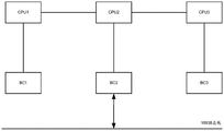
By applying the multiplexing data bus redundancy synchronous communication method, the modular system structure of the triple-modular redundancy computer is shown in fig. 7.
The communication bus chip has an output enable inhibit function and is controlled by the chip output inhibit hardware signal. The signal is connected to its corresponding CPU module through hardware. The CPU module numbers are 1, 2 and 3 respectively, only one host computer is provided, and the number 1 host computer is defaulted at the initial electrification. Working modes of 1553B communication bus chips of the three devices are BC modes, only the output prohibition signal of the host chip is low, and the bus output is enabled; the output of the other two chips is high, and the bus output is forbidden. If the host is abnormal, the host right is transferred from the machine No. 1 to the machine No. 2, at the moment, the machine No. 2 changes the output prohibition signal of the bus chip to be low, and simultaneously, the machine No. 1 changes the output prohibition signal of the bus chip to be high. Because the system has only one host at any time, the bus system is controlled by only one BC at any time, the control right can be seamlessly switched, at most, one message is abnormal, and the bus interface works uninterruptedly.
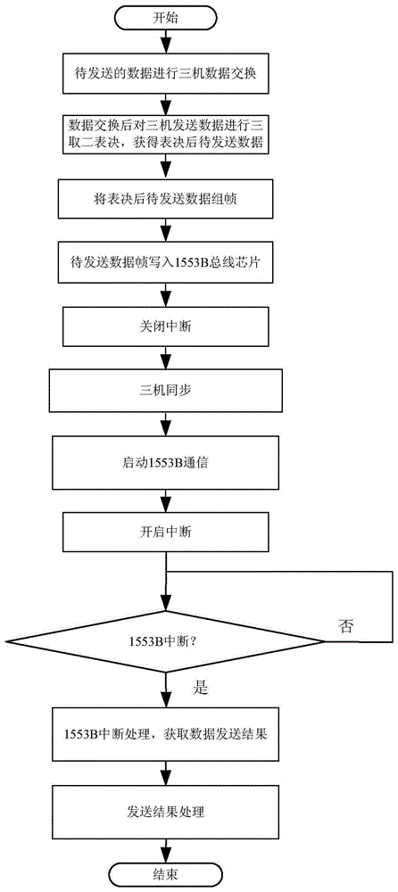
By applying the multiplexing data bus redundancy synchronous communication method, the process of sending data by the 1553B bus is shown in FIG. 8:
data exchange is carried out on data to be sent through a three-machine data exchange interface;
voting by two out of three after data exchange to obtain voted data;
the voted data is filled into a sending data 1553B message frame;
filling the combined 1553B message frame into a bus chip to prepare for starting bus communication;
the method needs to start bus communication and comprises the following steps: 1. closing the interrupt; 2. synchronizing the three machines; 3. starting 1553B bus communication; 4. starting an interrupt;
after waiting for 1553B bus communication interrupt return, reading out a state word of bus communication in the interrupt processing to obtain a data transmission result;
and carrying out corresponding processing according to the sending result.
By applying the multiplexing data bus redundancy synchronous communication method, the process of receiving data by the 1553B bus is shown in FIG. 9:
framing the acquired remote terminal data message, and writing the framed remote terminal data message into a 1553B bus chip;
and starting bus communication, wherein the starting step is the same as the process of sending data by the bus. Namely, the method comprises the following steps: 1. closing the interrupt; 2. synchronizing the three machines; 3. starting 1553B bus communication; 4. starting an interrupt;
after the 1553B bus communication interrupt returns, the bus communication data is read out in the interrupt processing, and the remote terminal data is obtained;
carrying out data exchange on received data;
voting the received data of the three-machine by two out of three after exchanging to obtain the received data after voting;
and correspondingly processing the received data.
According to the redundancy synchronous communication method for the multi-channel transmission data bus, interface hardware achieves complete triple modular redundancy and single point faults of the interface are completely eliminated. When the fault switching of the main computer is detected, the current task does not need to be interrupted, the task interruption caused by the recovery time required by the system when the bus communication interface is switched can be avoided, the serious consequence caused by the overlong failure time of the control system can be avoided, the reliability and the safety of the system can be improved, and the method can be suitable for the working environment with more severe task continuity.
In summary, the embodiments presented in connection with the figures are only preferred. Those skilled in the art can derive other alternative structures according to the design concept of the present invention, and the alternative structures should also fall within the scope of the solution of the present invention.