CN1125465C - Formation method and structure of word line decoder circuit in memory - Google Patents
Formation method and structure of word line decoder circuit in memory Download PDFInfo
- Publication number
- CN1125465C CN1125465C CN 98107762 CN98107762A CN1125465C CN 1125465 C CN1125465 C CN 1125465C CN 98107762 CN98107762 CN 98107762 CN 98107762 A CN98107762 A CN 98107762A CN 1125465 C CN1125465 C CN 1125465C
- Authority
- CN
- China
- Prior art keywords
- word line
- channel transistor
- regional
- metal oxide
- type
- Prior art date
- Legal status (The legal status is an assumption and is not a legal conclusion. Google has not performed a legal analysis and makes no representation as to the accuracy of the status listed.)
- Expired - Lifetime
Links
- 238000000034 method Methods 0.000 title claims abstract description 10
- 230000015572 biosynthetic process Effects 0.000 title 1
- 239000004065 semiconductor Substances 0.000 claims abstract description 27
- 229910044991 metal oxide Inorganic materials 0.000 claims description 44
- 150000004706 metal oxides Chemical class 0.000 claims description 44
- 108090000699 N-Type Calcium Channels Proteins 0.000 claims description 9
- 102000004129 N-Type Calcium Channels Human genes 0.000 claims description 9
- 238000010586 diagram Methods 0.000 description 7
- 238000002955 isolation Methods 0.000 description 3
- 108010075750 P-Type Calcium Channels Proteins 0.000 description 2
- 238000012986 modification Methods 0.000 description 2
- 230000004048 modification Effects 0.000 description 2
- XUIMIQQOPSSXEZ-UHFFFAOYSA-N Silicon Chemical compound [Si] XUIMIQQOPSSXEZ-UHFFFAOYSA-N 0.000 description 1
- 238000004519 manufacturing process Methods 0.000 description 1
- 239000002184 metal Substances 0.000 description 1
- 230000002040 relaxant effect Effects 0.000 description 1
- 229910052710 silicon Inorganic materials 0.000 description 1
- 239000010703 silicon Substances 0.000 description 1
Images



Landscapes
- Semiconductor Memories (AREA)
Abstract
Description
本发明有关于半导体存储器,特别有关于减少区域字线解码器的半导体面积。This invention relates to semiconductor memory, and more particularly to reducing the semiconductor area of a local wordline decoder.
参考图1,该图示出依据现有技术的二个区域字线解码器,而一区域字线解码器具有三个晶体管。如图1所示,其表示用来解码区域字线0的一电路100及用来解码区域字线1的一电路110。p型沟道晶体管(P1)101及n型沟道晶体管(N1)102在字线驱动输入107和一参考电位109之间以串联形式连接在一起。输入(mw1n0)104连接到晶体管101与102的栅极。输出(1w10)106连接到晶体管101及102的连接处。n型沟道晶体管(N11)103的漏极和源极分别连接于输出106和参考电位109。晶体管103的栅极连接到输入(w1drn)108,此输入(w1drn)108的信号与字线驱动输入107的信号反相。Referring to FIG. 1, this figure shows a two-area wordline decoder according to the prior art, while a one-area wordline decoder has three transistors. As shown in FIG. 1 , a circuit 100 for decoding local wordline 0 and a circuit 110 for decoding
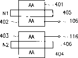
现参考图2,该图示出图1中电路的实际布置。晶体管(P1)101、(N1)102、(N11)103、(P2)111、(N2)112及(N21)113以二列三行方式排列。尺寸Y是由存储器单元间的距离所决定的。参考图3,其表示出晶体管N1和N2的更详细的布置。401和402为晶体管N1的有源区(AA)或n型区域(源极或漏极)。区域405为晶体管N1的金属氧化物栅极。403和404为晶体管N2的有源区(AA)或n型区域(源极或漏极)。区域406为晶体管N2的金属氧化物栅极。n型区域402和403分别连接到输出(1w10)106及输出(1w11)116。Reference is now made to FIG. 2 which shows the actual arrangement of the circuit in FIG. 1 . The transistors (P1) 101, (N1) 102, (N11) 103, (P2) 111, (N2) 112 and (N21) 113 are arranged in two columns and three rows. The dimension Y is determined by the distance between memory cells. Referring to Figure 3, a more detailed arrangement of transistors N1 and N2 is shown. 401 and 402 are the active area (AA) or n-type area (source or drain) of transistor N1.
美国专利5,446,698(McClure)针对区域字线的一多余全域字线而公开,但区域字线解码器的细节并没有被讨论。美国专利5,587,960(FERRIS)公开一具有副位线的半导体存储器,但是并没有讨论副字线解码器的细节。US Patent 5,446,698 (McClure) discloses a redundant global word line for local word lines, but the details of the local word line decoder are not discussed. US Patent 5,587,960 (FERRIS) discloses a semiconductor memory with sub-bit lines, but does not discuss the details of sub-word line decoders.
本发明的第一目的是提供一可减少存储器中区域字线解码器的半导体面积的方法和电路,用于在半导体存储器中的一第一区域字线解码器和第二区域字线解码器间共享一n型金属氧化物半导体,该方法包括步骤:提供具有一第一区域字线的一第一区域字线解码器;提供具有一第二区域字线的一第二区域字线解码器;提供一n型沟道金属氧化物半导体器件;将该n型沟道金属氧化物半导体器件连接于该第一区域字线和该第二区域字线之间;以及在该第一区域字线解码器和该第二区域字线解码器之间共享该n型沟道金属氧化物半导体器件。The first object of the present invention is to provide a method and circuit which can reduce the semiconductor area of the regional word line decoder in the memory, and is used between a first regional word line decoder and a second regional word line decoder in the semiconductor memory Sharing an n-type metal oxide semiconductor, the method includes the steps of: providing a first regional word line decoder with a first regional word line; providing a second regional word line decoder with a second regional word line; providing an n-channel metal oxide semiconductor device; connecting the n-channel metal oxide semiconductor device between the first regional word line and the second regional word line; and decoding the first regional word line The n-channel metal oxide semiconductor device is shared between the device and the second region word line decoder.
本发明的第二目的提供一种具有可供一第一区域字线解码器和第二区域字线解码器共享的一n型金属氧化物半导体的一字解码器电路,包括:一参考电位;一第一区域字线解码器,用来起动一第一区域字线,具有一输入(mw1n0)、输入(w1dr)及输出(1w10),该第一区域字线解码器起动该输出(1w10);一第二区域字线解码器,用来起动一第二区域字线,其具有一输入(mw1n1)、输入(w1dr)及输出(1w11),该第二区域字线解码器起动该输出(1w11);以及一n型金属氧化物半导体器件,它连接于该第一区域字线解码器的输出(1w10)和该第二区域字线解码器的输出(1w11)之间,且具有一输入(w1drn)。根据该解码电路,可减少存储器晶片的面积。The second object of the present invention is to provide a word decoder circuit with an n-type metal oxide semiconductor shared by a word line decoder in a first region and a word line decoder in a second region, comprising: a reference potential; A first regional wordline decoder for enabling a first regional wordline having an input (mw1n0), an input (w1dr) and an output (1w10), the first regional wordline decoder enabling the output (1w10) ; a second regional word line decoder for enabling a second regional word line having an input (mw1n1), input (w1dr) and output (1w11), the second regional word line decoder enabling the output ( 1w11); and an n-type metal oxide semiconductor device connected between the output (1w10) of the first regional word line decoder and the output (1w11) of the second regional word line decoder, and having an input (w1drn). According to this decoding circuit, the area of the memory chip can be reduced.
本发明的第三目的提供一种具有可供一第一区域字线解码器和第二区域字线解码器共享的一n型金属氧化物半导体的一字线解码器电路的结构,包括:一第一n型沟道晶体管,其具有一第一n型区域、第二n型区域及第一金属氧化物栅极,所述第一n型区域借助所述第一金属氧化物栅极而与所述第二n型区域隔离;一第二n型沟道晶体管,其具有一第三n型区域、第四n型区域及第二金属氧化物栅极,所述第三n型区域借助所述第二金属氧化物栅极而与所述第四n型区域隔离;以及一第三n型沟道晶体管,其具有该第二n型区域、第三n型区域及第三金属氧化物栅极,所述第二n型区域借助所述第三金属氧化物栅极而与所述第三n型区域隔离;一第一p型沟道晶体管,其具有一第一p型区域、第二p型区域及第一金属氧化物栅极;以及一第二p型沟道晶体管,其具有一第三p型区域、第四p型区域及第二金属氧化物栅极;其中所述第一p型沟道晶体管靠近所述第一n型沟道晶体管,所述第二p型沟道晶体管靠近所述第二n型沟道晶体管。根据该结构,可改善存储器单元的运用。The third object of the present invention provides a structure of a word line decoder circuit having an n-type metal oxide semiconductor shared by a first region word line decoder and a second region word line decoder, comprising: a The first n-type channel transistor has a first n-type region, a second n-type region and a first metal oxide gate, and the first n-type region is connected with the first metal oxide gate by means of the first metal oxide gate The second n-type region is isolated; a second n-type channel transistor has a third n-type region, a fourth n-type region and a second metal oxide gate, and the third n-type region is said second metal oxide gate isolated from said fourth n-type region; and a third n-channel transistor having said second n-type region, a third n-type region and a third metal oxide gate pole, the second n-type region is isolated from the third n-type region by the third metal oxide gate; a first p-type channel transistor has a first p-type region, a second A p-type region and a first metal oxide gate; and a second p-channel transistor having a third p-type region, a fourth p-type region and a second metal oxide gate; wherein the first A p-channel transistor is adjacent to the first n-channel transistor, and the second p-channel transistor is adjacent to the second n-channel transistor. According to this structure, utilization of the memory cell can be improved.
本发明上述的目的可借助去除具有三个晶体管的区域字线解码器中的一个晶体管,以及加入可供二个区域字线解码器共用的第五个晶体管来达到。因上述第五个晶体管被安置在二个已存在的晶体管之间而不会增加任何面积,所以被去除的两个晶体管所占用的面积可不再需要。The above object of the present invention can be achieved by eliminating one transistor in the local word line decoder having three transistors, and adding a fifth transistor which can be shared by two local word line decoders. Since the above-mentioned fifth transistor is placed between the two existing transistors without increasing any area, the area occupied by the removed two transistors is no longer needed.
为让本发明的上述目的、特征、和优点能更明显易懂,下文特举一较佳实施例,并配合所附附图,作详细说明如下,附图中,In order to make the above-mentioned purposes, features, and advantages of the present invention more obvious and understandable, a preferred embodiment is specifically cited below, together with the accompanying drawings, and described in detail as follows. In the drawings,
图1示出用以说明依据现有技术的字线解码器的电路图;FIG. 1 shows a circuit diagram illustrating a word line decoder according to the prior art;
图2示出用以说明图1中字线解码器的实际布置;Figure 2 shows the actual arrangement for illustrating the word line decoder in Figure 1;
图3示出用以说明图2的部分详细示意图;Fig. 3 shows a partial detailed schematic diagram for explaining Fig. 2;
图4示出用以说明本发明的高阶方框图;Figure 4 shows a high level block diagram illustrating the present invention;
图5示出用以说明依据本发明一较佳实施例的字线解码器的电路图;FIG. 5 shows a circuit diagram for illustrating a word line decoder according to a preferred embodiment of the present invention;
图6示出图5中电路的输入和输出信号图;Fig. 6 shows the input and output signal diagram of the circuit in Fig. 5;
图7示出用以说明图5中电路的实际字线解码器布置;以及Figure 7 shows the actual wordline decoder arrangement used to illustrate the circuit in Figure 5; and
图8示出用以说明图7的部分详细示意图。FIG. 8 shows a partial detailed schematic diagram for explaining FIG. 7 .
符号说明:Symbol Description:
100为用来解码区域字线0的电路、110为用来解码区域字线1的电路、101为晶体管(P1)、102为晶体管(N1)、103为晶体管(N11)、111为晶体管(P2)、112为晶体管(N2)、113为晶体管(N21)、104为主要字线输入φ(mw1n0)、106为区域字线输出φ(1w10)、107为字线驱动输入(w1dr)、108为字线反相驱动输入(w1drn)、109为参考电位、114为主要字线输入I(mw1n1)、116为区域字线输出I(1w11)、131为晶体管(N3)、501为第一区域字线解码器、502为第二区域字线解码器、503为NMOS器件、401和402为晶体管(N1)的有源区(AA)、405为晶体管N1的金属氧化物栅极、403和404为晶体管(N2)的有源区(AA)、406为晶体管(N2)的金属氧化物栅极、曲线1为主要字线输入φ(mw1n0)上的信号、曲线2为主要字线输入I(mw1n1)上的信号、曲线3为字线驱动输入(w1dr)107上的信号、曲线4为字线反相驱动输入(w1drn)108上的信号、曲线5为区域字线输出φ(1w10)106上的信号、曲线6为区域字线输出I(1w11)116的信号。100 is a circuit for decoding local word line 0, 110 is a circuit for decoding
实施例Example
参考图4,该图示出在一半导体存储器中第一区域字线解码器和第二区域字线解码器共用一n型沟道金属氧化物半导体(NMOS)器件。方块501为具有一第一区域字线(1w10)106做为输出的一第一区域字线解码器。方块502为具有一第二区域字线(1w11)116做为输出的一第二区域字线解码器。接下来,方块503为连接于上述第一区域字线(1w10)106和第二区域字线(1w11)116之间的NMOS器件。因此,方块503由第一区域字线解码器和第二区域字线解码器共用,其参与第一区域字线和第二区域字线的解码。Referring to FIG. 4, this figure shows that a first-region wordline decoder and a second-region wordline decoder share an n-channel metal-oxide-semiconductor (NMOS) device in a semiconductor memory. Block 501 is a first local word line decoder having a first local word line (1w10) 106 as output. Block 502 is a second local word line decoder having a second local word line (1w11) 116 as output. Next, block 503 is an NMOS device connected between the above-mentioned first regional word line ( 1w10 ) 106 and second regional word line ( 1w11 ) 116 . Therefore, block 503 is shared by the first regional word line decoder and the second regional word line decoder, which participates in the decoding of the first regional word line and the second regional word line.
现参考图5,该图示出依据本发明一较佳实施例的电路图。解码器500包括二个区域字线解码器501、502以及器件503。第一区域字线解码器501具有一主要字线输入φ(mw1n0)104、p型沟道晶体管(P1)101、n型沟道晶体管(N1)102及第一区域字线输出φ(1w10)106,用来将第一主要字线解码。第二区域字线解码器502具有一主要字线输入I(mw1n1)114、晶体管(P2)111、晶体管(N2)112及第二区域字线输出I(1w11)116,用来将第二主要字线解码。器件503为一n型沟道晶体管,它连接于输出(1w10)与输出(1w11)之间,并为这二个输出的解码所共享。Referring now to FIG. 5, this figure shows a circuit diagram according to a preferred embodiment of the present invention. The decoder 500 includes two local wordline decoders 501 , 502 and a device 503 . The first regional word line decoder 501 has a main word line input φ(mw1n0) 104, a p-type channel transistor (P1) 101, an n-type channel transistor (N1) 102 and a first regional word line output φ(1w10) 106, used to decode the first main word line. The second local word line decoder 502 has a main word line input I (mw1n1) 114, a transistor (P2) 111, a transistor (N2) 112 and a second local word line output I (1w11) 116, which are used to convert the second main word line Word line decoding. Device 503 is an n-channel transistor connected between output (1w10) and output (1w11) and shared by the decoding of these two outputs.
p型沟道晶体管(P1)101和n型沟道晶体管(N1)102以串联形式连接于字线驱动输入(w1dr)107及一参考电位109之间。p型沟道晶体管(P2)111与n型沟道晶体管(N2)112也具有相同的连接方式。晶体管101和102的栅极连接到输入104,而晶体管111及112的栅极连接到输入114。输出106连接到晶体管101和102的连接处。输出116连接到晶体管111和112的连接处。n型沟道晶体管(N3)131的源极和漏极分别连接到第一区域字输出φ(1w10)106和第二区域字输出I(1w11)116,而n型沟道晶体管(N3)131的栅极连接于字线反相驱动输入(w1drn)108。A p-channel transistor ( P1 ) 101 and an n-channel transistor ( N1 ) 102 are connected in series between a word line drive input ( w1dr ) 107 and a reference potential 109 . The p-channel transistor (P2) 111 and the n-channel transistor (N2) 112 also have the same connection method. The gates of
现参考图6,该图示出图5中电路的输入及输出信号。曲线1和2分别代表输入(mw1n0)104及输入(mw1n1)114上的信号,其中输入(mw1n1)114为一固定电位Vh。曲线3和4分别代表字线驱动输入(w1dr)107及字线反相驱动输入(w1drn)108上的信号。曲线5表示出由于图5中的电路解码结果,而使得输出(1w10)106在一周期间为一正电位。在本范围例中,因为区域字线解码器502没有被选择,所以曲线6显示输出(1w11)116为0电位。Reference is now made to FIG. 6, which shows the input and output signals of the circuit of FIG.
现参考图7,该图示出图5的电路在一硅晶片上的晶体管排列。晶体管(P1)101、(N1)102、(P2)111及(N2)112为正交排列,其中晶体管(P1)和(P2)在同一行,而晶体管(N1)及(N2)是在另外一相邻行。此外,晶体管(P1)及(N1)是在同一列上,而晶体管(P2)和(N2)是在另外一相邻列上。一n型晶体管(N3)131夹于晶体管(N1)和晶体管(N2)之间。值得注意的,是为节约空间,在本发明中已删除现有晶体管(N11)103及(N21)113所占的第三行。Referring now to FIG. 7, this figure shows the transistor arrangement of the circuit of FIG. 5 on a silicon wafer. Transistors (P1) 101, (N1) 102, (P2) 111 and (N2) 112 are arranged orthogonally, wherein transistors (P1) and (P2) are in the same row, and transistors (N1) and (N2) are in another an adjacent row. Furthermore, transistors (P1) and (N1) are on the same column, and transistors (P2) and (N2) are on another adjacent column. An n-type transistor (N3) 131 is sandwiched between the transistor (N1) and the transistor (N2). It should be noted that for saving space, the third row occupied by the existing transistors (N11) 103 and (N21) 113 has been deleted in the present invention.
参考图8,该图示出晶体管(N1)、(N2)及(N3)的详细布置图。区域401和402代表电晶(N1)的有源区(AA)或n型区域(源极和漏极),区域405为晶体管(N1)的金属氧化物栅极,其连接到输入(mw1n0)104。区域403和404为晶体管(N2)的有源区(AA)或n型区域(源极和漏极)。区域406为晶体管(N2)的金属氧化物栅极,其连接到输入(mw1n1)114。晶体管(N2)131利用区域402和403做为其源极和漏极而安置于区域(AA)或n型区域402和403之间。因为插入n型沟道晶体管N3,所以区域402和403不需有隔离程序,因此可放宽n型隔离规则以及可改善合格率。金属氧化物栅极407放置于区域402及403之间,成为晶体管(N3)的栅极。金属氧化物栅极407是连接输入(w1drn)108。n型区域402及403分别连接到输出(1w10)106和(1w11)116。因此晶体管N3不需要额外的空间,而每一区域字线解码器几乎只需用到二个晶体管所需的布置空间。Referring to Figure 8, this figure shows a detailed layout of transistors (N1), (N2) and (N3).
从图7和图8可明显了解,用来隔离n型区域的金属氧化物栅极彼此平行。同样地,n型区域也是彼此平行,并且平行于上述金属氧化物栅极。晶体管(P1)和(P2)的结构和上述n型沟道晶体管(N1)和(N2)相似,其具有对应于源极和漏极的p型区域及用来将此p型区域隔离的金属氧化物栅极。此外,p型沟道晶体管(P1)和(P2)和n型沟道晶体管(N1)和(N2)彼此靠近。It is obvious from FIG. 7 and FIG. 8 that the metal oxide gates used to isolate the n-type region are parallel to each other. Likewise, the n-type regions are also parallel to each other and parallel to the aforementioned metal oxide gate. Transistors (P1) and (P2) are similar in structure to the n-channel transistors (N1) and (N2) above, with p-type regions corresponding to the source and drain and metal to isolate the p-type regions oxide gate. Furthermore, p-channel transistors (P1) and (P2) and n-channel transistors (N1) and (N2) are close to each other.
本发明的优点是可减少区域字线解码器的尺寸,进而减少晶片面积及借助放宽n型隔离规则来改善存储器单元的运用,进而改善合格率。当半导体制程进入到0.35μm和0.25μm制程时,晶体管的尺寸比字线间距以更快速度缩小之际,上述本发明所提出的改善显得更为重要。因为需要很多解码器电路,所以需减少使用区域字线的解码器的尺寸。The invention has the advantages of reducing the size of the regional word line decoder, thereby reducing the chip area and improving the utilization of the memory unit by relaxing the n-type isolation rule, thereby improving the qualified rate. When the semiconductor manufacturing process enters the 0.35 μm and 0.25 μm process, the size of the transistor shrinks at a faster rate than the pitch of the word line, the improvement proposed by the above-mentioned invention becomes more important. Since many decoder circuits are required, the size of the decoder using the local word lines needs to be reduced.
虽然本发明已以一较佳实施例揭露如上,然而该实施例并非用以限定本发明,任何熟习此项技术的人员,在不脱离本发明的精神和范围的情况下,可对其做出各种更动与润饰,而本发明的保护范围以后附的权利所限定的为准。Although the present invention has been disclosed as above with a preferred embodiment, this embodiment is not intended to limit the present invention, any person skilled in the art can make changes to it without departing from the spirit and scope of the present invention. Various modifications and modifications, and the protection scope of the present invention shall prevail as defined by the appended rights.
Claims (11)
Priority Applications (1)
| Application Number | Priority Date | Filing Date | Title |
|---|---|---|---|
| CN 98107762 CN1125465C (en) | 1998-04-29 | 1998-04-29 | Formation method and structure of word line decoder circuit in memory |
Applications Claiming Priority (1)
| Application Number | Priority Date | Filing Date | Title |
|---|---|---|---|
| CN 98107762 CN1125465C (en) | 1998-04-29 | 1998-04-29 | Formation method and structure of word line decoder circuit in memory |
Publications (2)
| Publication Number | Publication Date |
|---|---|
| CN1233835A CN1233835A (en) | 1999-11-03 |
| CN1125465C true CN1125465C (en) | 2003-10-22 |
Family
ID=5219447
Family Applications (1)
| Application Number | Title | Priority Date | Filing Date |
|---|---|---|---|
| CN 98107762 Expired - Lifetime CN1125465C (en) | 1998-04-29 | 1998-04-29 | Formation method and structure of word line decoder circuit in memory |
Country Status (1)
| Country | Link |
|---|---|
| CN (1) | CN1125465C (en) |
Families Citing this family (3)
| Publication number | Priority date | Publication date | Assignee | Title |
|---|---|---|---|---|
| CN100454440C (en) * | 2002-07-31 | 2009-01-21 | 连邦科技股份有限公司 | Combined SRAM and mask ROM memory cell |
| CN106469563B (en) * | 2015-08-17 | 2018-12-18 | 旺宏电子股份有限公司 | Array Architecture with Region Decoders |
| KR102586179B1 (en) * | 2018-10-04 | 2023-10-10 | 에스케이하이닉스 주식회사 | Semiconductor device |
-
1998
- 1998-04-29 CN CN 98107762 patent/CN1125465C/en not_active Expired - Lifetime
Also Published As
| Publication number | Publication date |
|---|---|
| CN1233835A (en) | 1999-11-03 |
Similar Documents
| Publication | Publication Date | Title |
|---|---|---|
| US7280425B2 (en) | Dual gate oxide one time programmable (OTP) antifuse cell | |
| JP5035335B2 (en) | SRAM device | |
| US20090168483A1 (en) | Ultra low voltage and minimum operating voltage tolerant register file | |
| KR20180131416A (en) | Content addressable memory and semiconductor device | |
| US20060145266A1 (en) | Semiconductor integrated circuit | |
| US20120258593A1 (en) | Sram cell with t-shaped contact | |
| CN1125465C (en) | Formation method and structure of word line decoder circuit in memory | |
| US5896344A (en) | Local word line decoder for memory with 2 1/2 MOS devices | |
| US7872893B2 (en) | Semiconductor memory device | |
| US8674411B2 (en) | Semiconductor device employing circuit blocks having the same characteristics | |
| CN110400797B (en) | SRAM memory cell structure layout, SRAM memory cell structure and layout thereof | |
| US5227996A (en) | Semiconductor memory device having word line driver | |
| CN117375595A (en) | A switching structure that reduces the leakage current of parasitic body diodes of MOS transistors | |
| JPH11162173A (en) | A method and a structure of a local word line decoder circuit which has an n-type metal oxide semiconductor device in a memory and can be shared by a first local word line decoder and a second local word line decoder | |
| JP3301398B2 (en) | Semiconductor storage device | |
| JP2591907B2 (en) | Decode circuit for read-only semiconductor memory device | |
| US20250292848A1 (en) | Encoded read-only memory and decoder | |
| JP4509765B2 (en) | MOS type semiconductor integrated circuit device | |
| WO2025193337A1 (en) | Encoded read-only memory and decoder | |
| US6847579B2 (en) | Semiconductor memory device | |
| KR20030031435A (en) | Semiconductor device using scl circuit | |
| WO2025076674A1 (en) | Switch structure for reducing leakage current of parasitic body diode of mos transistor | |
| JPS59186196A (en) | Horizontal ratioless ROM | |
| JP3749294B2 (en) | Decoder circuit for semiconductor memory device | |
| TW201314689A (en) | Non-volatile memory programming method |
Legal Events
| Date | Code | Title | Description |
|---|---|---|---|
| C06 | Publication | ||
| PB01 | Publication | ||
| C10 | Entry into substantive examination | ||
| SE01 | Entry into force of request for substantive examination | ||
| C14 | Grant of patent or utility model | ||
| GR01 | Patent grant | ||
| ASS | Succession or assignment of patent right |
Owner name: TAIWAN SEMICONDUCTOR MFG Free format text: FORMER OWNER: WORLD ADVANCED INTEGRATED CIRCUIT STOCK-SHARING CO., LTD. Effective date: 20120529 |
|
| C41 | Transfer of patent application or patent right or utility model | ||
| TR01 | Transfer of patent right |
Effective date of registration: 20120529 Address after: Hsinchu Science Park, Taiwan, China Patentee after: Taiwan Semiconductor Mfg Address before: Hsinchu Science Park, Taiwan, China Patentee before: World Advanced Integrated circuit stock-sharing Co., Ltd. |
|
| CX01 | Expiry of patent term | ||
| CX01 | Expiry of patent term |
Granted publication date: 20031022 |