CN1126151C - 有硅化物层的半导体器件的制造方法 - Google Patents
有硅化物层的半导体器件的制造方法 Download PDFInfo
- Publication number
- CN1126151C CN1126151C CN98120147A CN98120147A CN1126151C CN 1126151 C CN1126151 C CN 1126151C CN 98120147 A CN98120147 A CN 98120147A CN 98120147 A CN98120147 A CN 98120147A CN 1126151 C CN1126151 C CN 1126151C
- Authority
- CN
- China
- Prior art keywords
- refractory metal
- metal film
- film
- nitrogen
- silicide layer
- Prior art date
- Legal status (The legal status is an assumption and is not a legal conclusion. Google has not performed a legal analysis and makes no representation as to the accuracy of the status listed.)
- Expired - Fee Related
Links
Images
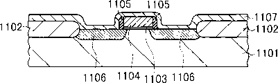
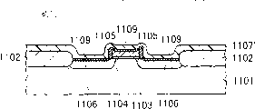


Classifications
-
- H—ELECTRICITY
- H10—SEMICONDUCTOR DEVICES; ELECTRIC SOLID-STATE DEVICES NOT OTHERWISE PROVIDED FOR
- H10D—INORGANIC ELECTRIC SEMICONDUCTOR DEVICES
- H10D30/00—Field-effect transistors [FET]
- H10D30/01—Manufacture or treatment
- H10D30/021—Manufacture or treatment of FETs having insulated gates [IGFET]
- H10D30/0212—Manufacture or treatment of FETs having insulated gates [IGFET] using self-aligned silicidation
-
- H—ELECTRICITY
- H10—SEMICONDUCTOR DEVICES; ELECTRIC SOLID-STATE DEVICES NOT OTHERWISE PROVIDED FOR
- H10D—INORGANIC ELECTRIC SEMICONDUCTOR DEVICES
- H10D64/00—Electrodes of devices having potential barriers
- H10D64/01—Manufacture or treatment
- H10D64/011—Manufacture or treatment of electrodes ohmically coupled to a semiconductor
- H10D64/0111—Manufacture or treatment of electrodes ohmically coupled to a semiconductor to Group IV semiconductors
- H10D64/0112—Manufacture or treatment of electrodes ohmically coupled to a semiconductor to Group IV semiconductors using conductive layers comprising silicides
-
- H—ELECTRICITY
- H10—SEMICONDUCTOR DEVICES; ELECTRIC SOLID-STATE DEVICES NOT OTHERWISE PROVIDED FOR
- H10D—INORGANIC ELECTRIC SEMICONDUCTOR DEVICES
- H10D64/00—Electrodes of devices having potential barriers
- H10D64/01—Manufacture or treatment
- H10D64/013—Manufacture or treatment of electrodes having a conductor capacitively coupled to a semiconductor by an insulator
- H10D64/01302—Manufacture or treatment of electrodes having a conductor capacitively coupled to a semiconductor by an insulator the insulator being formed after the semiconductor body, the semiconductor being silicon
- H10D64/01304—Manufacture or treatment of electrodes having a conductor capacitively coupled to a semiconductor by an insulator the insulator being formed after the semiconductor body, the semiconductor being silicon characterised by the conductor
- H10D64/01306—Manufacture or treatment of electrodes having a conductor capacitively coupled to a semiconductor by an insulator the insulator being formed after the semiconductor body, the semiconductor being silicon characterised by the conductor the conductor comprising a layer of silicon contacting the insulator, e.g. polysilicon
- H10D64/01308—Manufacture or treatment of electrodes having a conductor capacitively coupled to a semiconductor by an insulator the insulator being formed after the semiconductor body, the semiconductor being silicon characterised by the conductor the conductor comprising a layer of silicon contacting the insulator, e.g. polysilicon the conductor further comprising a non-elemental silicon additional conductive layer, e.g. a metal silicide layer formed by the reaction of silicon with an implanted metal
- H10D64/0131—Manufacture or treatment of electrodes having a conductor capacitively coupled to a semiconductor by an insulator the insulator being formed after the semiconductor body, the semiconductor being silicon characterised by the conductor the conductor comprising a layer of silicon contacting the insulator, e.g. polysilicon the conductor further comprising a non-elemental silicon additional conductive layer, e.g. a metal silicide layer formed by the reaction of silicon with an implanted metal the additional conductive layer comprising a silicide layer formed by the silicidation reaction between the layer of silicon with a metal layer which is not formed by metal implantation
-
- H—ELECTRICITY
- H10—SEMICONDUCTOR DEVICES; ELECTRIC SOLID-STATE DEVICES NOT OTHERWISE PROVIDED FOR
- H10D—INORGANIC ELECTRIC SEMICONDUCTOR DEVICES
- H10D64/00—Electrodes of devices having potential barriers
- H10D64/01—Manufacture or treatment
- H10D64/013—Manufacture or treatment of electrodes having a conductor capacitively coupled to a semiconductor by an insulator
- H10D64/01302—Manufacture or treatment of electrodes having a conductor capacitively coupled to a semiconductor by an insulator the insulator being formed after the semiconductor body, the semiconductor being silicon
- H10D64/01304—Manufacture or treatment of electrodes having a conductor capacitively coupled to a semiconductor by an insulator the insulator being formed after the semiconductor body, the semiconductor being silicon characterised by the conductor
- H10D64/01318—Manufacture or treatment of electrodes having a conductor capacitively coupled to a semiconductor by an insulator the insulator being formed after the semiconductor body, the semiconductor being silicon characterised by the conductor the conductor comprising a layer of alloy material, compound material or organic material contacting the insulator, e.g. TiN
- H10D64/0132—Manufacture or treatment of electrodes having a conductor capacitively coupled to a semiconductor by an insulator the insulator being formed after the semiconductor body, the semiconductor being silicon characterised by the conductor the conductor comprising a layer of alloy material, compound material or organic material contacting the insulator, e.g. TiN the conductor being a metallic silicide
-
- H—ELECTRICITY
- H10—SEMICONDUCTOR DEVICES; ELECTRIC SOLID-STATE DEVICES NOT OTHERWISE PROVIDED FOR
- H10D—INORGANIC ELECTRIC SEMICONDUCTOR DEVICES
- H10D64/00—Electrodes of devices having potential barriers
- H10D64/60—Electrodes characterised by their materials
- H10D64/66—Electrodes having a conductor capacitively coupled to a semiconductor by an insulator, e.g. MIS electrodes
- H10D64/661—Electrodes having a conductor capacitively coupled to a semiconductor by an insulator, e.g. MIS electrodes the conductor comprising a layer of silicon contacting the insulator, e.g. polysilicon having vertical doping variation
- H10D64/662—Electrodes having a conductor capacitively coupled to a semiconductor by an insulator, e.g. MIS electrodes the conductor comprising a layer of silicon contacting the insulator, e.g. polysilicon having vertical doping variation the conductor further comprising additional layers, e.g. multiple silicon layers having different crystal structures
- H10D64/663—Electrodes having a conductor capacitively coupled to a semiconductor by an insulator, e.g. MIS electrodes the conductor comprising a layer of silicon contacting the insulator, e.g. polysilicon having vertical doping variation the conductor further comprising additional layers, e.g. multiple silicon layers having different crystal structures the additional layers comprising a silicide layer contacting the layer of silicon, e.g. polycide gates
-
- H—ELECTRICITY
- H10—SEMICONDUCTOR DEVICES; ELECTRIC SOLID-STATE DEVICES NOT OTHERWISE PROVIDED FOR
- H10P—GENERIC PROCESSES OR APPARATUS FOR THE MANUFACTURE OR TREATMENT OF DEVICES COVERED BY CLASS H10
- H10P14/00—Formation of materials, e.g. in the shape of layers or pillars
- H10P14/40—Formation of materials, e.g. in the shape of layers or pillars of conductive or resistive materials
- H10P14/42—Formation of materials, e.g. in the shape of layers or pillars of conductive or resistive materials using a gas or vapour
- H10P14/44—Physical vapour deposition [PVD]
Landscapes
- Electrodes Of Semiconductors (AREA)
- Insulated Gate Type Field-Effect Transistor (AREA)
- Internal Circuitry In Semiconductor Integrated Circuit Devices (AREA)
Applications Claiming Priority (3)
| Application Number | Priority Date | Filing Date | Title |
|---|---|---|---|
| JP277604/1997 | 1997-10-09 | ||
| JP27760497A JP3248570B2 (ja) | 1997-10-09 | 1997-10-09 | 半導体装置の製造方法 |
| JP277604/97 | 1997-10-09 |
Publications (2)
| Publication Number | Publication Date |
|---|---|
| CN1214534A CN1214534A (zh) | 1999-04-21 |
| CN1126151C true CN1126151C (zh) | 2003-10-29 |
Family
ID=17585749
Family Applications (1)
| Application Number | Title | Priority Date | Filing Date |
|---|---|---|---|
| CN98120147A Expired - Fee Related CN1126151C (zh) | 1997-10-09 | 1998-10-09 | 有硅化物层的半导体器件的制造方法 |
Country Status (6)
| Country | Link |
|---|---|
| US (1) | US6127267A (fr) |
| EP (1) | EP0908935A3 (fr) |
| JP (1) | JP3248570B2 (fr) |
| KR (1) | KR100280244B1 (fr) |
| CN (1) | CN1126151C (fr) |
| TW (1) | TW389943B (fr) |
Families Citing this family (22)
| Publication number | Priority date | Publication date | Assignee | Title |
|---|---|---|---|---|
| TW452982B (en) | 1998-10-05 | 2001-09-01 | Seiko Epson Corp | Semiconductor device and method for producing the same |
| US6759315B1 (en) * | 1999-01-04 | 2004-07-06 | International Business Machines Corporation | Method for selective trimming of gate structures and apparatus formed thereby |
| JP2000332241A (ja) * | 1999-05-20 | 2000-11-30 | Nec Corp | 半導体装置の製造方法 |
| JP4774568B2 (ja) * | 1999-10-01 | 2011-09-14 | ソニー株式会社 | 半導体装置の製造方法 |
| US6281086B1 (en) * | 1999-10-21 | 2001-08-28 | Advanced Micro Devices, Inc. | Semiconductor device having a low resistance gate conductor and method of fabrication the same |
| JP3554514B2 (ja) * | 1999-12-03 | 2004-08-18 | 松下電器産業株式会社 | 半導体装置及びその製造方法 |
| US6767835B1 (en) | 2002-04-30 | 2004-07-27 | Advanced Micro Devices, Inc. | Method of making a shaped gate electrode structure, and device comprising same |
| US7943594B2 (en) * | 2002-07-10 | 2011-05-17 | Massachusetts Institute Of Technology | Solid-phase and solution-phase synthesis of glycosylphosphatidylinositol glycans |
| UY28886A1 (es) * | 2004-05-10 | 2005-12-30 | Boehringer Ingelheim Int | Anticuerpos que consisten en polipéptidos y derivados conprendiendo tres secuencias conteniendo respectivamente los siguientes números de seq. id: 1-3 y 4-6; 7-9 y 10-12 y 13-15 ó 16-18 |
| US7235472B2 (en) * | 2004-11-12 | 2007-06-26 | Infineon Technologies Ag | Method of making fully silicided gate electrode |
| CN100416778C (zh) * | 2005-07-20 | 2008-09-03 | 上海华虹Nec电子有限公司 | 超大规模集成电路难熔金属硅化物的形成方法 |
| JP2008244059A (ja) * | 2007-03-27 | 2008-10-09 | Renesas Technology Corp | 半導体装置の製造方法 |
| JP5423269B2 (ja) * | 2009-09-15 | 2014-02-19 | 富士通セミコンダクター株式会社 | 半導体装置とその製造方法 |
| US9076823B2 (en) * | 2013-09-11 | 2015-07-07 | Taiwan Semiconductor Manufacturing Company, Ltd. | Bi-layer metal deposition in silicide formation |
| WO2017026485A1 (fr) | 2015-08-11 | 2017-02-16 | 東レバッテリーセパレータフィルム株式会社 | Séparateur de batterie |
| JP6766411B2 (ja) | 2016-03-31 | 2020-10-14 | 東レ株式会社 | 電池用セパレータおよびその製造方法 |
| WO2017199468A1 (fr) | 2016-05-16 | 2017-11-23 | 株式会社アルバック | Procédé de formation de film de régulation des contraintes internes |
| EP3493296A4 (fr) | 2016-07-28 | 2020-04-29 | Toray Industries, Inc. | Corps enroulé multicouche |
| WO2018124176A1 (fr) | 2016-12-27 | 2018-07-05 | 東レ株式会社 | Séparateur de pile, corps d'électrode et pile rechargeable à électrolyte non aqueux |
| WO2018168835A1 (fr) | 2017-03-17 | 2018-09-20 | 東レ株式会社 | Séparateur de piles, corps d'électrode et pile secondaire à électrolyte non aqueux |
| JP2020047711A (ja) * | 2018-09-18 | 2020-03-26 | 株式会社アルバック | 記憶素子製造方法 |
| CN110850609A (zh) * | 2019-11-21 | 2020-02-28 | 中国电子科技集团公司第二十六研究所 | 一种低应力声光器件及其制备方法 |
Family Cites Families (10)
| Publication number | Priority date | Publication date | Assignee | Title |
|---|---|---|---|---|
| US4923822A (en) * | 1989-05-22 | 1990-05-08 | Hewlett-Packard Company | Method of fabricating a semiconductor device by capping a conductive layer with a nitride layer |
| US5326724A (en) * | 1991-12-27 | 1994-07-05 | Texas Instruments Incorporated | Oxide-capped titanium silicide formation |
| US5365111A (en) * | 1992-12-23 | 1994-11-15 | Advanced Micro Devices, Inc. | Stable local interconnect/active area silicide structure for VLSI applications |
| JP3280803B2 (ja) * | 1994-08-18 | 2002-05-13 | 沖電気工業株式会社 | 半導体装置及びその製造方法 |
| US5593924A (en) * | 1995-06-02 | 1997-01-14 | Texas Instruments Incorporated | Use of a capping layer to attain low titanium-silicide sheet resistance and uniform silicide thickness for sub-micron silicon and polysilicon lines |
| JP2850883B2 (ja) * | 1995-10-28 | 1999-01-27 | 日本電気株式会社 | 半導体装置の製造方法 |
| JP2900897B2 (ja) * | 1995-10-28 | 1999-06-02 | 日本電気株式会社 | 半導体装置の製造方法 |
| JP3734559B2 (ja) * | 1996-03-15 | 2006-01-11 | 富士通株式会社 | 半導体装置の製造方法 |
| US5902129A (en) * | 1997-04-07 | 1999-05-11 | Lsi Logic Corporation | Process for forming improved cobalt silicide layer on integrated circuit structure using two capping layers |
| US6022795A (en) * | 1998-05-07 | 2000-02-08 | United Microelectronics Corp. | Salicide formation process |
-
1997
- 1997-10-09 JP JP27760497A patent/JP3248570B2/ja not_active Expired - Fee Related
-
1998
- 1998-10-01 TW TW087116414A patent/TW389943B/zh active
- 1998-10-02 EP EP98118655A patent/EP0908935A3/fr not_active Withdrawn
- 1998-10-09 KR KR1019980042226A patent/KR100280244B1/ko not_active Expired - Fee Related
- 1998-10-09 US US09/168,670 patent/US6127267A/en not_active Expired - Fee Related
- 1998-10-09 CN CN98120147A patent/CN1126151C/zh not_active Expired - Fee Related
Also Published As
| Publication number | Publication date |
|---|---|
| JPH11121399A (ja) | 1999-04-30 |
| US6127267A (en) | 2000-10-03 |
| EP0908935A2 (fr) | 1999-04-14 |
| TW389943B (en) | 2000-05-11 |
| JP3248570B2 (ja) | 2002-01-21 |
| EP0908935A3 (fr) | 1999-09-08 |
| CN1214534A (zh) | 1999-04-21 |
| KR19990036981A (ko) | 1999-05-25 |
| KR100280244B1 (ko) | 2001-03-02 |
Similar Documents
| Publication | Publication Date | Title |
|---|---|---|
| CN1214534A (zh) | 有硅化物层的半导体器件的制造方法 | |
| CN1234156C (zh) | 绝缘膜的形成方法和半导体装置的制造方法 | |
| CN1291500C (zh) | 半导体器件及其制备方法 | |
| CN100352016C (zh) | 半导体器件及其制造方法 | |
| CN1222986C (zh) | 半导体装置的制造方法和半导体装置 | |
| CN1110007A (zh) | 具有接触结构的半导体器件及其制造方法 | |
| CN1282230C (zh) | 半导体装置的制造方法及半导体装置 | |
| CN1485891A (zh) | 半导体存储器件及其制造方法 | |
| CN1183580C (zh) | 半导体装置的制造方法和半导体装置 | |
| CN1118864C (zh) | 利用相变来制造半导体器件的方法 | |
| CN1107344C (zh) | 利用有选择的外延生长方法的半导体器件制造方法 | |
| CN1219771A (zh) | 半导体器件及其制造方法 | |
| CN1449585A (zh) | 半导体器件及其制造方法 | |
| CN1881548A (zh) | 半导体器件制造方法 | |
| CN1893114A (zh) | 具有铁电膜作为栅极绝缘膜的半导体器件及其制造方法 | |
| CN1284217C (zh) | 半导体器件的制造方法 | |
| CN1879209A (zh) | 半导体装置及其制造方法 | |
| CN1763973A (zh) | 半导体装置及其制造方法 | |
| CN1967787A (zh) | 基底绝缘膜的形成方法 | |
| CN1849705A (zh) | 用于分别优化在同一半导体芯片内的pmos和nmos晶体管的薄栅极电介质的方法以及由此制造的器件 | |
| CN1230769A (zh) | 半导体器件制造方法 | |
| CN1838434A (zh) | 半导体器件及其制造方法 | |
| CN1945835A (zh) | 半导体装置及其制造方法 | |
| CN1518090A (zh) | 半导体器件的制造方法 | |
| CN1237620C (zh) | 半导体装置和半导体装置的制造方法 |
Legal Events
| Date | Code | Title | Description |
|---|---|---|---|
| C10 | Entry into substantive examination | ||
| SE01 | Entry into force of request for substantive examination | ||
| C06 | Publication | ||
| PB01 | Publication | ||
| ASS | Succession or assignment of patent right |
Owner name: NEC ELECTRONICS TAIWAN LTD. Free format text: FORMER OWNER: NIPPON ELECTRIC CO., LTD. Effective date: 20030403 |
|
| C41 | Transfer of patent application or patent right or utility model | ||
| TA01 | Transfer of patent application right |
Effective date of registration: 20030403 Address after: Kanagawa, Japan Applicant after: NEC Corp. Address before: Tokyo, Japan Applicant before: NEC Corp. |
|
| C14 | Grant of patent or utility model | ||
| GR01 | Patent grant | ||
| C19 | Lapse of patent right due to non-payment of the annual fee | ||
| CF01 | Termination of patent right due to non-payment of annual fee |