CN112866169A - Transmission scheme for SC-FDMA with two DFT precoding levels - Google Patents
Transmission scheme for SC-FDMA with two DFT precoding levels Download PDFInfo
- Publication number
- CN112866169A CN112866169A CN202110368328.9A CN202110368328A CN112866169A CN 112866169 A CN112866169 A CN 112866169A CN 202110368328 A CN202110368328 A CN 202110368328A CN 112866169 A CN112866169 A CN 112866169A
- Authority
- CN
- China
- Prior art keywords
- data stream
- symbols
- mapping
- dft0
- fec
- Prior art date
- Legal status (The legal status is an assumption and is not a legal conclusion. Google has not performed a legal analysis and makes no representation as to the accuracy of the status listed.)
- Pending
Links
- 230000005540 biological transmission Effects 0.000 title description 8
- 238000000034 method Methods 0.000 claims abstract description 26
- 238000004891 communication Methods 0.000 claims abstract description 13
- 238000013507 mapping Methods 0.000 claims description 21
- 125000004122 cyclic group Chemical group 0.000 claims description 20
- 238000012937 correction Methods 0.000 claims description 10
- 238000010586 diagram Methods 0.000 description 24
- 238000003780 insertion Methods 0.000 description 11
- 230000037431 insertion Effects 0.000 description 11
- 230000003595 spectral effect Effects 0.000 description 7
- 230000001413 cellular effect Effects 0.000 description 4
- 230000000116 mitigating effect Effects 0.000 description 4
- 239000013256 coordination polymer Substances 0.000 description 3
- 230000000694 effects Effects 0.000 description 3
- 238000005516 engineering process Methods 0.000 description 3
- 239000000969 carrier Substances 0.000 description 2
- 230000002452 interceptive effect Effects 0.000 description 2
- 238000001228 spectrum Methods 0.000 description 2
- 230000007423 decrease Effects 0.000 description 1
- 238000013461 design Methods 0.000 description 1
- PCHJSUWPFVWCPO-UHFFFAOYSA-N gold Chemical compound [Au] PCHJSUWPFVWCPO-UHFFFAOYSA-N 0.000 description 1
- 239000010931 gold Substances 0.000 description 1
- 229910052737 gold Inorganic materials 0.000 description 1
- 230000001788 irregular Effects 0.000 description 1
- 230000007774 longterm Effects 0.000 description 1
- 238000012986 modification Methods 0.000 description 1
- 230000004048 modification Effects 0.000 description 1
- 230000010363 phase shift Effects 0.000 description 1
- 230000011664 signaling Effects 0.000 description 1
Images


Classifications
-
- H—ELECTRICITY
- H04—ELECTRIC COMMUNICATION TECHNIQUE
- H04L—TRANSMISSION OF DIGITAL INFORMATION, e.g. TELEGRAPHIC COMMUNICATION
- H04L27/00—Modulated-carrier systems
- H04L27/26—Systems using multi-frequency codes
- H04L27/2601—Multicarrier modulation systems
- H04L27/2626—Arrangements specific to the transmitter only
- H04L27/2627—Modulators
- H04L27/2634—Inverse fast Fourier transform [IFFT] or inverse discrete Fourier transform [IDFT] modulators in combination with other circuits for modulation
- H04L27/2636—Inverse fast Fourier transform [IFFT] or inverse discrete Fourier transform [IDFT] modulators in combination with other circuits for modulation with FFT or DFT modulators, e.g. standard single-carrier frequency-division multiple access [SC-FDMA] transmitter or DFT spread orthogonal frequency division multiplexing [DFT-SOFDM]
-
- H—ELECTRICITY
- H04—ELECTRIC COMMUNICATION TECHNIQUE
- H04B—TRANSMISSION
- H04B7/00—Radio transmission systems, i.e. using radiation field
- H04B7/02—Diversity systems; Multi-antenna system, i.e. transmission or reception using multiple antennas
- H04B7/04—Diversity systems; Multi-antenna system, i.e. transmission or reception using multiple antennas using two or more spaced independent antennas
- H04B7/0413—MIMO systems
- H04B7/0456—Selection of precoding matrices or codebooks, e.g. using matrices antenna weighting
-
- H—ELECTRICITY
- H04—ELECTRIC COMMUNICATION TECHNIQUE
- H04L—TRANSMISSION OF DIGITAL INFORMATION, e.g. TELEGRAPHIC COMMUNICATION
- H04L1/00—Arrangements for detecting or preventing errors in the information received
- H04L1/004—Arrangements for detecting or preventing errors in the information received by using forward error control
- H04L1/0041—Arrangements at the transmitter end
-
- H—ELECTRICITY
- H04—ELECTRIC COMMUNICATION TECHNIQUE
- H04L—TRANSMISSION OF DIGITAL INFORMATION, e.g. TELEGRAPHIC COMMUNICATION
- H04L1/00—Arrangements for detecting or preventing errors in the information received
- H04L1/004—Arrangements for detecting or preventing errors in the information received by using forward error control
- H04L1/0045—Arrangements at the receiver end
Landscapes
- Engineering & Computer Science (AREA)
- Computer Networks & Wireless Communication (AREA)
- Signal Processing (AREA)
- Physics & Mathematics (AREA)
- Discrete Mathematics (AREA)
- General Physics & Mathematics (AREA)
- Mathematical Physics (AREA)
- Mobile Radio Communication Systems (AREA)
- Transmitters (AREA)
Abstract
Embodiments of the present application relate to methods of operating a communication system. In described examples, the method of operating a wireless communication system includes receiving first and second parallel data streams. By having NDFT0A Discrete Fourier Transform (DFT) of size (510) converts the first data stream to a first frequency-domain data stream, where N isDFT0Is a positive integer. By having NDFT1The size (511) DFT converts the second data stream to a second frequency-domain data stream, where NDFT1Is a positive integer. The first and second frequency-domain data streams are mapped to respective subcarriers (512).
Description
The present application is a divisional application of the invention patent application entitled "transmission scheme for SC-FDMA with two DFT precoding levels", application No. 201680006733.3, filed 2016, 1, 22 days.
Background
The present invention relates generally to wireless communication systems, and more particularly to single carrier frequency domain multiple access (SC-FDMA) systems with multiple DFT precoding levels.
Increased data demand in cellular networks has led to the deployment of small cells that provide Long Term Evolution (LTE) connectivity for a number of users that is less than the number of users typically served by a macro cell. This allows both greater transmission/reception resource opportunities for the user and relieves the macro network of burden. The entire 3GPP release 10-12 puts a considerable focus on standardization efforts on the technical challenges of the Radio Access Network (RAN) of small cells. This is a difficult technical challenge especially for outdoor small cell deployments due to the irregular location of small cell sites such as lampposts, signposts, bus stops and traffic signals.
The LTE radio access technology, also known as evolved universal terrestrial radio access network (E-UTRAN), has been standardized by the 3GPP working group. Orthogonal Frequency Division Multiple Access (OFDMA) and SC-FDMA schemes are selected for the Downlink (DL) and Uplink (UL) of E-UTRAN, respectively. User Equipment (UE) is time and frequency multiplexed on a Physical Uplink Shared Channel (PUSCH) and a Physical Uplink Control Channel (PUCCH), and time and frequency synchronization between UEs ensures optimal intra-cell orthogonality. The LTE air interface provides the best spectral efficiency and cost tradeoff of the latest cellular network standards, and has therefore been widely adopted by operators as a unique 4G technology for Radio Access Networks (RANs), making it a robust and proven technology. Since the trend in RAN topology is to increase cell density by adding small cells in the vicinity of legacy macro cells, the associated backhaul link density increases accordingly, and the difference between RAN and backhaul wireless channels also decreases. Several special problems are associated with small cell sites, for exampleSuch as high reliability and 10-6Packet Error Rate (PER) requirements, sparse spectrum availability, critical latency, cost, and relaxed peak-to-average power ratio (PAPR). The behavior of the small cell site also differs from the RAN in that there is no handover, remote units do not connect and disconnect at the same rate as User Equipment (UE), and non line of sight (NLOS) Remote Units (RU) small cell sites are non-mobile.
Previous improvements in small cell topology have provided significant improvements in data throughput, but further improvements are possible.
Disclosure of Invention
In a first embodiment, a method of operating a wireless communication system includes receiving a first data stream and passing the first data stream having NDFT0A Discrete Fourier Transform (DFT) of size converts it to a first frequency-domain data stream, where N isDFT0Is a positive integer. The method further includes receiving a second data stream in parallel with the first data stream. By having NDFT1The sized DFT converts the second data stream to a second frequency-domain data stream, where NDFT1Is a positive integer. The first and second frequency-domain data streams are mapped to respective subcarriers.
In a second embodiment, a method of operating a wireless communication system includes receiving a parallel data stream having first and second portions. By having a size NDFT0Converts the first portion into a first time-domain data stream, where N is Inverse Discrete Fourier Transform (IDFT)DFT0Is a positive integer. By having a size NDFT1The IDFT of (a) converts the second portion into a second time-domain data stream, where N isDFT1Is a positive integer.
In a third embodiment, a method of operating a wireless communication system includes encoding a serial data stream with a Forward Error Correction (FEC) code to produce FEC encoded data. Mapping the FEC encoded data into a series of symbols. Phase pilot symbols are inserted into the series of symbols.
Drawings
Fig. 1 is a diagram of a wireless communication system having a cellular macro site hosting a backhaul point-to-multipoint (P2MP) Hub Unit (HU) serving a Remote Unit (RU) that relays communication between a small cell and a plurality of User Equipments (UEs).
Fig. 2 is a diagram of a subset of a frame configuration.
Fig. 3 is a diagram of a conventional baseband transmitter.
Fig. 4 is a table showing 50 predetermined Discrete Fourier Transform (DFT) or Inverse Discrete Fourier Transform (IDFT) sizes and their corresponding indices.
Fig. 5A is a diagram of a baseband transmitter with two separate DFT precoding stages.
Fig. 5B is a diagram of a baseband receiver with two separate IDFT decoding stages.
FIGS. 6A-6D are tables showing predetermined DFT/IDFT sizes for respective system bandwidths of 5MHz, 10MHz, 15MHz, and 20 MHz.
Fig. 7A is a diagram of a baseband transmitter with two separate and parallel DFT precoding stages.
Fig. 7B is a diagram of a baseband receiver with two separate and parallel IDFT decoding stages.
Fig. 8A is a diagram of a baseband transmitter with time domain phase pilot symbol insertion.
Fig. 8B is a diagram of a baseband receiver with Phase Noise Mitigation (PNM).
Fig. 8C is a diagram of a baseband transmitter with time-domain phase pilot symbol insertion and two separate DFT precoding stages.
Fig. 8D is a diagram of a baseband transmitter with time-domain phase pilot symbol insertion and two separate and parallel DFT precoding stages.
Fig. 9A is a diagram of a phase pilot symbol generator circuit that may be used in fig. 8A, 8C, or 8D.
Fig. 9B is a diagram showing phase pilot symbols inserted within 48 QAM symbols.
Detailed Description
Fig. 1 shows an NLOS Time Division Duplex (TDD) wireless backhaul system according to an example embodiment. The cellular macro site 100 hosts a macro base station. The macro site 100 also hosts a wireless backhaul Hub Unit (HU). The macro site 100 is connected to a small cell site, such as small cell site 104. Each small cell site is co-located with a small cell base station and a wireless backhaul Remote Unit (RU). The macro site 100 communicates with the small cell sites via backhaul links (e.g., backhaul link 110) through a point-to-multipoint (P2MP) wireless backhaul system. The base stations of the macro site 100 communicate directly with the UE 102 via the RAN link 112. However, the UE 106 communicates directly with the small cell base station of the small cell site 104 via the RAN access link 108. The RU of small cell site 104, in turn, communicates directly with the HU of macro cell site 100 via backhaul link 110. The system is designed to maximize spectral reuse. The backhaul link 110 design utilizes a Transmission Time Interval (TTI) based on 0.5ms slots to minimize latency and 5ms UL and DL frames for compatibility with TD-LTE. Alternative embodiments may use different frame durations and TTIs based on different slots.
Fig. 2 illustrates UL/ DL frame configurations 1, 3, and 5. Each frame has a duration of 5ms and is slot-based rather than subframe-based. Each frame has 10 (0-9) slots. Each slot has a duration of 0.5 ms. Of course, alternative embodiments may use different frame durations and different slot-based Transmission Time Intervals (TTIs). Here, D indicates a downlink slot, and U indicates an uplink slot. In each of the three UL/DL configurations, slot 3 is a special slot indicated by S. This fixed location of the special time slot ensures backward compatibility with TD-LTE frames. It advantageously permits always to find NLOS UL/DL configurations that are 100% compatible with any 5ms period TD-LTE UL/DL subframe configuration. For example, this prevents NLOS backhaul DL transmissions from interfering with TD-LTE RAN UL transmissions on the access link (when both are operating on the same frequency). In other words, it advantageously prevents a transmitter at a macrocell site 100 of one system from interfering with a receiver of a co-located system.
Fig. 3 is a diagram of a conventional baseband transmitter. In the present discussion, any reference to circuitry may include circuitry formed from hardware, software, or a combination of hardware and software. The baseband transmitter of fig. 3 receives a data signal and adds a Cyclic Redundancy Check (CRC) block. The data is then encoded or pre-coded by a Forward Error Correction (FEC) encoder and scrambled by a scrambling circuit. The scrambled data is mapped to the appropriate symbol constellation and converted to a parallel data stream. A Discrete Fourier Transform (DFT) pre-coding stage converts the data to the frequency domain and applies it to Subcarrier (SC) mapping circuitry along with control channel and other Physical (PHY) channel data. The parallel data stream is then converted back to time domain data and to a serial data stream. A cyclic prefix is appended to the serial data stream. The resulting output data of the time slot is conceptually represented on the right with time as the horizontal axis and frequency as the vertical axis. The slot is preferably 0.5ms in duration with seven SC-FDMA symbols. The first SC-FDMA symbol is a pilot signal that transmits a predefined frequency-domain signal to assist the receiver in performing channel estimation. The last six SC-FDMA symbols in time are used for the data channel. The bandwidth of the slot may be from 5MHz to 20MHz and include upper and lower subcarriers reserved for control channels at each end of the frequency band. The space between the control channel and the pilot signal/data channel indicates the subcarriers that may not be used. This may occur when a specific size DFT is not supported. Which frequently occurs when a small number of UEs or RUs are assigned to available radio resources and reduces spectral efficiency.
One problem with conventional DFT circuitry is that it must be limited to discrete sizes. This is because DFT operations are typically implemented in hardware due to high data throughput requirements. Of course, the same limitations apply to the receiver and its corresponding Inverse Discrete Fourier Transform (IDFT), as will be discussed in detail. Fig. 4 is a table showing 50 predetermined Discrete Fourier Transform (DFT) or Inverse Discrete Fourier Transform (IDFT) sizes and their corresponding indices. These predetermined sizes are provided by Texas Instruments Incorporated in the Keystone (Keystone) family of its system on a chip (SoC) products. When a single transmit link or a small number of transmit links are assigned to a large frequency band, it is possible that the entire spectrum cannot be filled and some subcarriers are not used for communication. For example, an LTE 20MHz system has 1200 subcarriers with a 15kHz subcarrier spacing. If the control channel (fig. 3) needs to include 12 subcarriers above and 12 below the data channel, 1176 subcarriers are still available for the data channel. The DFT index 41 (fig. 4) is used for the data channel, but the 24 subcarriers (1200-24-1152 ═ 24) remain unused. Therefore, the spectral efficiency of the communication system is less than optimal.
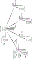
Fig. 5A is a diagram of a baseband transmitter according to a first embodiment with two separate DFT precoding stages. The baseband transmitter of fig. 5A receives a data signal and adds a Cyclic Redundancy Check (CRC) block 500. The data is then encoded or pre-encoded by a Forward Error Correction (FEC) encoder 502 and scrambled by a scrambling circuit 504. The scrambled data is mapped to the appropriate symbol constellation 506 and converted to a parallel data stream 508. Discrete Fourier Transform (DFT) circuits 510 and 511 convert the data to frequency domain signals and apply them to Subcarrier (SC) mapping circuit 512 along with control channel and other Physical (PHY) channel data. DFT circuit 510 uses a signal with NDFT0DFT index of 600 31. DFT circuit 511 using a DFT with NDFT1DFT index of 576. In overview, it allocates 1176 subcarriers to data channel 530 and all available subcarriers are used. The frequency domain data is applied to Subcarrier (SC) mapping circuit 512 along with control channels and other Physical (PHY) channel data. The parallel data stream is then converted back to time domain data 514 and to serial data stream 516. A cyclic prefix is appended to serial data stream 528. The resulting output data of the time slot 530 is conceptually represented on the right with time as the horizontal axis and frequency as the vertical axis. The upper portion of the data channel corresponds to N generated by DFT circuit 510DFT0Sub-carriers and the lower part of the data channel corresponds to N generated by DFT circuit 511DFT1A subcarrier. The embodiment of fig. 5A advantageously uses parallel DFT precoding stages 510 and 511 to fully use the available subcarriers, thereby maximizing spectral efficiency.
Fig. 5B is a diagram of a baseband receiver with two separate IDFT stages. Data 530 is applied to the baseband receiver and the Cyclic Prefix (CP)540 is removed. Serial to parallel circuit 542 converts the data into a parallel data stream that is applied to Fast Fourier Transform (FFT) circuit 544. The resulting frequency domain data is applied to a subcarrier demapping and equalization circuit 546. Here, the individual subcarriers are preferably equalized to compensate for the channel effect. Next, the equalized data is applied to an inverse discrete Fourier transformTransform (IDFT) circuits 548 and 549. IDFT circuitry 548 performs N corresponding to DFT circuitry 510DFT0600 transform. IDFT circuitry 549 performs N corresponding to DFT circuitry 511DFT1 Convert 576. The resulting time domain data is applied to a parallel to serial circuit 550. The resulting serial data stream is then applied to a symbol demapping circuit 552. Here, log-likelihood ratio (LLR) calculations are performed on the received and equalized QAM symbols to provide soft decision information for each information bit to an FEC decoder, such as a Turbo decoder. The resulting soft decision information is then descrambled 554 and applied to decoding circuitry 556. The resulting decoded data is then applied to a Cyclic Redundancy Check (CRC) circuit 558 to verify correct data reception.
The previous examples of fig. 5A and 5B advantageously utilize all 1200 subcarriers of a 20MHz bandwidth, with no unused or guard subcarriers. Data and control channel allocation sizes are specified as part of the air interface standard. Of course, other sizes of DFT and IDFT combinations are possible. For example, DFT circuit 510 may be used with N DFT01080, and the DFT circuitry 511 may use a DFT index 40 with NDFT1DFT index 11 of 96. Alternatively, DFT circuit 510 may be used with NDFT0The DFT index 37 of 960, and DFT circuitry 511 may use a DFT with N DFT1216 DFT index 18. In overview, however, the selected combinations each utilize 1176 subcarriers of the data channel 530.
Fig. 6A-6D are tables showing predetermined DFT/IDFT sizes for respective system bandwidths of 5MHz, 10MHz, 15MHz, and 20MHz, with 300, 600, 900, and 1200 system subcarriers, respectively. Embodiments preferably use the same table for DFT and IDFT allocations. Each row shows a respective PHY channel class and includes control channels, data channels, and unused or guard subcarrier allocations, as well as DFT0 and DFT1 sizes for the data channels. Each column shows various subcarrier allocations for a control channel having 2 or 4 Physical Resource Blocks (PRBs). There are four different control channel allocation sizes depending on the required amount of control information in each mode of operation. For maximum spectral efficiency, the sum of the control channel, data channel and guard subcarriers in each column should equal the system subcarriers of the corresponding system bandwidthThe total number of (a). N is a radical ofDFT0And NDFT1Is equal to the number of subcarriers in the data channel. The two selected DFT sizes of fig. 6A-6D of the parallel DFT precoding stages advantageously provide a minimum number of unused or guard subcarriers, thereby maximizing the spectral efficiency of the system. The previous examples of FIGS. 5A and 5B utilized N in the first column of FIG. 6D DFT0600 and NDFT1The assignment of 576. Furthermore, in some cases, only a single DFT and IDFT circuitry is necessary. For example, having NDFT0Only a single DFT pre-coding stage of 576 is necessary for a 10MHz bandwidth with 2 PRBs, as shown in the left column of fig. 6B. And has NDFT0Only a single DFT pre-coding stage of 1152 is necessary for a 20MHz bandwidth with 4 PRBs, as shown in the second column of fig. 6D. Finally, although only two DFT/IDFT sizes are provided by way of example, three or more DFT/IDFT sizes may be allocated to utilize all available subcarriers.
Fig. 7A is a diagram of a baseband transmitter according to a second embodiment with two separate and parallel DFT precoding stages. This embodiment provides two separate data channels each with its own respective transport block. Data channel 0 includes a CRC circuit 700 and an FEC encoder circuit 702, followed by a scrambling circuit 704. The scrambled data is symbol mapped by circuit 706 and applied to serial to parallel (S/P) circuit 708. The parallel data stream is then applied to a stream having a size NDFT0The DFT circuitry 710 as previously described. Data channel 1 is formed in parallel with data channel 0 and includes a CRC circuit 701 and an FEC encoder circuit 703, followed by a scrambling circuit 705. The scrambled data is symbol mapped by circuitry 707 and applied to S/P circuitry 709. The parallel data stream is then applied to a stream having a size NDFT1DFT circuitry 711 as previously described. The frequency domain data is applied to Subcarrier (SC) mapping circuit 712 along with control channels and other Physical (PHY) channel data. The parallel data stream is then converted back to time domain data 714 and to serial data stream 716. A cyclic prefix is appended to serial data stream 718. The resulting output data of time slot 730 is conceptually represented on the right with time as the horizontal axis and frequency as the vertical axis. Upper part (data letter)Lane 0) corresponds to N generated by DFT circuitry 710DFT0Sub-carriers and the lower part (data channel 2) corresponds to N generated by DFT circuit 711DFT1A subcarrier.
Fig. 7B is a diagram of a baseband receiver corresponding to the baseband transmitter of fig. 7A and having two separate and parallel IDFT stages. Data 730 is applied to the baseband receiver and the Cyclic Prefix (CP)740 is removed. Serial to parallel circuit 742 converts the data into a parallel data stream that is applied to Fast Fourier Transform (FFT) circuit 744. The resulting frequency domain data is applied to a subcarrier demapping and equalization circuit 746. Here, the individual subcarriers are preferably equalized to compensate for the channel effect. The equalized data is then applied to Inverse Discrete Fourier Transform (IDFT) circuits 748 and 749. IDFT circuitry 748 performs N corresponding to DFT circuitry 710 on data channel 0DFT0And (4) converting. IDFT circuitry 749 performs N corresponding to DFT circuitry 711 on data channel 1DFT1And (4) converting. The resulting time domain data is applied to parallel to serial circuits 750 and 751. The resulting serial data streams are each demapped by respective circuits 752 and 753. Here, log-likelihood ratio (LLR) calculations are performed on the received and equalized QAM symbols to provide soft decision information for each information bit to an FEC decoder (e.g., turbo decoder). The resulting soft decision information is then descrambled by respective circuits 754 and 755. The descrambled data streams are applied to respective decoding circuits 756 and 757. A Cyclic Redundancy Check (CRC) is performed on each data stream by respective circuits 758 and 759 to verify correct data reception.
The previous examples of fig. 7A and 7B advantageously utilize all subcarriers of a 5MHz to 20MHz bandwidth without expending additional hardware. The data and control channel allocation sizes are specified as part of the air interface standard so no additional software is required. The embodiments of fig. 7A and 7B are also suitable for separate data channels and their respective transport blocks.
Fig. 8A is a diagram of a baseband transmitter with time domain phase pilot symbol insertion. The baseband transmitter of fig. 8A receives a data signal and adds a Cyclic Redundancy Check (CRC) block 800. The data is then encoded or pre-coded by a Forward Error Correction (FEC) encoder 802 and scrambled by a scrambling circuit 804. The scrambled data is mapped to the appropriate symbol constellation 806. A Phase Pilot Symbol (PPS) generator 900 generates a sequence of phase pilot symbols that are inserted into the time domain data stream by phase pilot symbol insertion circuitry 808. The phase pilot symbols allow the receiver to estimate, track, and compensate for phase noise in the received QAM symbols. This achieves significant phase noise mitigation and is very important for advanced modulation schemes including 256-QAM or higher QAM. It is particularly advantageous in higher frequency bands, such as the 5GHz unlicensed band, the microwave band, and the millimeter wave band. The resulting data stream with phase pilot symbols is converted to a parallel data stream 810. Discrete Fourier Transform (DFT) circuitry 812 converts the data to the frequency domain and applies it to Subcarrier (SC) mapping circuitry 814 along with control channel and other Physical (PHY) channel data. The parallel data stream is then converted back to time domain data 816 and to a serial data stream 818. A cyclic prefix is appended to serial data stream 820.
Fig. 8B is a diagram of a baseband receiver that may be used with the baseband transmitter of fig. 8A. The data is applied to the baseband receiver and the Cyclic Prefix (CP)840 is removed. Serial to parallel circuit 842 converts the data into a parallel data stream that is applied to Fast Fourier Transform (FFT) circuit 844. The resulting frequency domain data is applied to a subcarrier demapping and equalization circuit 846. Here, the individual subcarriers are preferably equalized to compensate for the channel effect. The equalized data is then applied to an Inverse Discrete Fourier Transform (IDFT) circuit 848. IDFT circuitry 848 performs N corresponding to DFT circuitry 810IDFTAnd (4) converting. The resulting time domain data is applied to a parallel to serial circuit 850. The resulting serial data stream is then applied to Phase Noise Mitigation (PNM) circuitry 552. The PNM circuitry estimates and tracks the phase noise embedded in the received and equalized Quadrature Amplitude Modulation (QAM) symbols. The PNM circuitry uses the known phase pilot symbols 900 from the baseband transmitter to compensate for the embedded phase noise. The compensated QAM data stream is then applied to a symbol demapping circuit 854. The resulting information bits are then descrambled 856 and applied to decoding circuitry 858. The resulting decoded data is then applied to a Cyclic Redundancy Check (CRC) circuit 860 to verify correct data reception.
Fig. 8C is a diagram of a baseband transmitter with time-domain phase pilot symbol insertion with two separate DFT precoding stages. The precoded portion (800) and 806) of the baseband transmitter of fig. 8C operates as previously discussed with reference to fig. 8A. A Phase Pilot Symbol (PPS) generator 900 generates a sequence of phase pilot symbols that are inserted into the time domain data stream by phase pilot symbol insertion circuitry 808. The resulting data stream with phase pilot symbols is converted to a parallel data stream 810. Discrete Fourier Transform (DFT) circuits 812 and 813 convert the data to the frequency domain and apply it to Subcarrier (SC) mapping circuit 814 along with control channel and other Physical (PHY) channel data. DFT circuitry 812 performs NDFT0And (4) converting. DFT circuit 813 performs NDFT1And (4) converting. In overview, it allocates all available subcarriers to a data channel and all available subcarriers are used. The parallel data stream is then converted back to time domain data 816 and to a serial data stream 818. A cyclic prefix is appended to serial data stream 820.
Fig. 8D is a diagram of another embodiment of a baseband transmitter with time-domain phase pilot symbol insertion and two separate and parallel DFT precoding stages. As previously discussed with reference to fig. 7A, this embodiment provides two separate data channels each having its own respective transport block. Data channel 0 includes CRC circuit 800 and FEC encoder circuit 802, followed by scrambling circuit 804. The scrambled data is symbol mapped by circuitry 806 and applied to phase pilot insertion circuitry 808. Circuitry 808 inserts phase pilot symbols from PPS generator circuitry 900 into the serial data stream. Serial to parallel (S/P) circuit 810 converts this to a parallel data stream and applies it to a data stream having a size NDFT0DFT circuitry 812. Data channel 1 is formed in parallel with data channel 0 and includes CRC circuit 801 and FEC encoder circuit 803, followed by scrambling circuit 805. The scrambled data is symbol mapped by circuit 807 and applied to phase pilot insertion circuit 809. Circuitry 809 inserts phase pilot symbols from PPS generator circuitry 901 into the serial data stream. Serial to parallel (S/P) circuit 811 converts this to a parallel data stream and applies it to a data stream having a size NDFT1DFT circuitry 813. Will come from a numberThe resulting frequency domain data for channels 1 and 2 is applied to Subcarrier (SC) mapping circuit 814 along with control channel and other Physical (PHY) channel data. The parallel data stream is then converted back to time domain data 816 and to a serial data stream 818. A cyclic prefix is appended to the serial data stream 818.
Fig. 9A is a diagram of a Phase Pilot Symbol (PPS) generator circuit 900 or 901 that may be used in fig. 8A, 8C, or 8D. The PPS generator includes a pseudo-random noise (PN) generator circuit 902 that may be formed from one or more Linear Feedback Shift Registers (LFSRs) with appropriate feedback circuitry. The PN generator circuit 902 preferably generates a pseudo-random noise (PN) sequence, such as a gold code for a PPS symbol. The PPS generator includes a symbol mapper circuit 906 coupled to receive the PN sequence. The symbol mapper circuit 906 preferably bit maps the two PN sequences to Quadrature Phase Shift Keying (QPSK) symbols to form a PPS. Of course, the symbol mapper may be adapted to map the PN sequence bits to other symbols, such as QAM symbols. QPSK PPS is preferably generated at higher power than QAM data symbols to facilitate receiver phase noise mitigation under low SNR or poor channel conditions. The PPS generator also includes a seed circuit 904 coupled to receive the load signal. The active level of the load signal will initialize the sequence c at the beginning of each radio frameinitLoaded into the generator circuit 902. In a preferred embodiment, cinitCan be represented by the following equation [1 ]]And (4) defining.

Here, n isRUIs an index of a Remote Unit (RU) or other receiving unit as in FIG. 1, q is a binary codeword index, iDL,ULIs a binary index indicating a Downlink (DL) or Uplink (UL) sequence, and N is a cell ID of a wireless cell. Mark 2KIndicating the stage K of the LFSR receiving the initialization seed.
Fig. 9B is a diagram showing phase pilot symbols inserted within 48 QAM symbols. Inserting PPS to have a predetermined average length NPHPPhase pilot (PHP) block of (e.g., 48). Will NDFT/NPHPPhase pilot symbols are inserted into the PHP block. Preferably, each PPS is inserted such that NPHPThe/2-1 modulation symbol precedes PPS, and NPHPThe/2 modulation symbols are located after the PPS. For example, the left PHP block of fig. 9B includes 23 leading modulation symbols, one PPS, and 24 trailing modulation symbols, for a total of 48 symbols. Similarly, if the last PHP block has length NPHP,lastThen PPS is inserted such that NPHP,lastThe/2-1 modulation symbol precedes PPS, and NPHP,lastThe/2 modulation symbols are located after the PPS. In the example of fig. 9B, the PPS advantageously compensates for phase noise embedded in the QAM symbol stream with only a 2% overhead. The insertion of the PPS is preferably enabled or disabled independently for each RU or receiving unit through higher layer signaling.
Modifications are possible in the described embodiments, and other embodiments are possible within the scope of the claims. Embodiments may be implemented in software, hardware, or a combination of both.
Claims (20)
1. A method of operating a communication system, comprising:
receiving a first data stream;
by having NDFT0A Discrete Fourier Transform (DFT) of size converts the first data stream to a first frequency-domain data stream, where N isDFT0Is a positive integer;
receiving a second data stream in parallel with the first data stream;
by having NDFT1The sized DFT converts the second data stream to a second frequency-domain data stream, where NDFT1Is a positive integer; and
the first and second frequency-domain data streams are mapped to respective subcarriers.
2. The method of claim 1, comprising mapping the first and second frequency-domain data streams with other physical channel data to respective subcarriers.
3. The method of claim 1, comprising passing a beam having NFFTAn inverse fast Fourier transform of size converts the respective subcarriers to a time-domain data stream, where NFFTGreater than or equal to NDFT0And NDFT1The sum of (1).
4. The method of claim 3, comprising adding a cyclic prefix to the time-domain data stream.
5. The method of claim 1, comprising:
receiving an input data stream;
encoding the input data stream with a forward error correction code, FEC, to produce an FEC encoded data stream;
mapping the FEC encoded data stream into a plurality of data symbols; and
the first and second data streams are generated from the plurality of data symbols.
6. The method of claim 4, comprising scrambling the FEC encoded data stream prior to the mapping step.
7. The method of claim 1, comprising selecting NDFT0And NDFT1To minimize the number of unused subcarriers.
8. The method of claim 1, comprising:
receiving a first input data stream;
encoding the first input data stream with a first forward error correction code, FEC, to produce a first FEC encoded data stream;
mapping the first FEC encoded data stream into a first plurality of data symbols;
generating the first data stream from the first plurality of data symbols;
receiving a second input data stream in parallel with the first input data stream;
encoding the second input data stream with a second forward error correction code, FEC, to produce a second FEC encoded data stream;
mapping the second FEC encoded data stream into a second plurality of data symbols; and
generating the second data stream from the second plurality of data symbols.
9. The method of claim 8, comprising:
scrambling said first FEC encoded data stream prior to said step of mapping said first FEC encoded data stream; and
scrambling the second FEC encoded data stream prior to said step of mapping the second FEC encoded data stream.
10. A method of operating a communication system, comprising:
receiving first and second portions of a data stream in parallel;
by having a size NDFT0The Inverse Discrete Fourier Transform (IDFT) of (2) converts the first portion into a first time-domain data stream, where N isDFT0Is a positive integer; and
by having a size NDFT1The IDFT of (a) converts the second portion into a second time-domain data stream, where N isDFT1Is a positive integer.
11. The method of claim 10, comprising:
by having a size NFFTTo generate parallel subcarrier streams, where N isFFTIs a positive integer, and wherein NFFTGreater than or equal to NDFT0And NDFT1The sum of (1); and
the subcarriers are demapped and equalized to produce the first and second portions.
12. The method of claim 11, wherein NFFTGreater than NDFT0And NDFT1The sum of (1).
13. The method of claim 10, comprising:
demapping symbols of the first and second time domain data streams to generate a serial data stream;
FEC decoding a forward error correction code of the serial data stream; and
performing a cyclic redundancy check on the decoded serial data stream.
14. The method of claim 13, comprising descrambling the serial data stream prior to the decoding step.
15. The method of claim 10, comprising removing a cyclic prefix prior to the step of receiving first and second portions of a data stream.
16. The method of claim 10, comprising:
demapping symbols of the first time domain data stream to produce a first serial data stream;
FEC decoding a forward error correction code of the first serial data stream;
performing a cyclic redundancy check on the decoded first serial data stream;
demapping symbols of the second time domain data stream to produce a second serial data stream;
forward Error Correction (FEC) decoding the second serial data stream; and
performing a cyclic redundancy check on the decoded second serial data stream.
17. The method of claim 16, comprising:
descrambling said first serial data stream prior to said step of FEC decoding said first serial data stream; and
descrambling the second serial data stream prior to the step of FEC decoding the second serial data stream.
18. A method of operating a communication system, comprising:
mapping the first data stream into a first series of Quadrature Amplitude Modulation (QAM) symbols;
generating a first pseudo-random noise (PN) sequence;
mapping a plurality of bits of the first PN sequence to first phase pilot symbols;
inserting the first phase pilot symbols into the first series of QAM symbols;
by having N after the inserting stepDFT0A Discrete Fourier Transform (DFT) of size converts the first data stream to a first frequency-domain data stream, where N isDFT0Is a positive integer;
mapping the first frequency-domain data streams to respective first subcarriers; and
by having a size NFFTThe corresponding first subcarrier is converted into a first time-domain data stream by an Inverse Discrete Fourier Transform (IDFT), where NFFTIs a positive integer.
19. The method of claim 18, comprising generating the first PN sequence in response to a remote unit RU index, a codeword index, a cell identification, and at least one of a downlink DL or uplink UL index.
20. The method of claim 18, comprising:
mapping the second data stream into a second series of QAM symbols;
generating a second pseudo-random noise PN sequence;
mapping a plurality of bits of the second PN sequence to second phase pilot symbols;
inserting the second phase pilot symbols into the second series of QAM symbols;
by having NDFT1A Discrete Fourier Transform (DFT) of size to convert the second data stream to a second frequency-domain data stream, where NDFT1Is a positive integer; and
mapping the second frequency-domain data streams to respective second subcarriers.
Applications Claiming Priority (5)
| Application Number | Priority Date | Filing Date | Title |
|---|---|---|---|
| US201562107038P | 2015-01-23 | 2015-01-23 | |
| US62/107,038 | 2015-01-23 | ||
| US14/971,624 | 2015-12-16 | ||
| US14/971,624 US10454739B2 (en) | 2015-01-23 | 2015-12-16 | Transmission scheme for SC-FDMA with two DFT-precoding stages |
| CN201680006733.3A CN107912081B (en) | 2015-01-23 | 2016-01-22 | Transmission scheme for SC-FDMA with two DFT precoding stages |
Related Parent Applications (1)
| Application Number | Title | Priority Date | Filing Date |
|---|---|---|---|
| CN201680006733.3A Division CN107912081B (en) | 2015-01-23 | 2016-01-22 | Transmission scheme for SC-FDMA with two DFT precoding stages |
Publications (1)
| Publication Number | Publication Date |
|---|---|
| CN112866169A true CN112866169A (en) | 2021-05-28 |
Family
ID=56417928
Family Applications (2)
| Application Number | Title | Priority Date | Filing Date |
|---|---|---|---|
| CN201680006733.3A Active CN107912081B (en) | 2015-01-23 | 2016-01-22 | Transmission scheme for SC-FDMA with two DFT precoding stages |
| CN202110368328.9A Pending CN112866169A (en) | 2015-01-23 | 2016-01-22 | Transmission scheme for SC-FDMA with two DFT precoding levels |
Family Applications Before (1)
| Application Number | Title | Priority Date | Filing Date |
|---|---|---|---|
| CN201680006733.3A Active CN107912081B (en) | 2015-01-23 | 2016-01-22 | Transmission scheme for SC-FDMA with two DFT precoding stages |
Country Status (5)
| Country | Link |
|---|---|
| US (2) | US10454739B2 (en) |
| EP (1) | EP3300548B1 (en) |
| JP (3) | JP2018511194A (en) |
| CN (2) | CN107912081B (en) |
| WO (1) | WO2016118929A2 (en) |
Families Citing this family (9)
| Publication number | Priority date | Publication date | Assignee | Title |
|---|---|---|---|---|
| JP6509890B2 (en) | 2013-11-11 | 2019-05-08 | エルジー エレクトロニクス インコーポレイティド | Broadcast signal transmitting apparatus, broadcast signal receiving apparatus, broadcast signal transmitting method and broadcast signal receiving method |
| EP3379787B1 (en) * | 2017-03-22 | 2023-08-09 | Mitsubishi Electric R&D Centre Europe B.V. | Reference signal for phase tracking insertion |
| US10700907B2 (en) * | 2017-07-12 | 2020-06-30 | Qualcomm Incorporated | Waveform for millimeter wave new radio |
| US10841143B2 (en) * | 2017-12-12 | 2020-11-17 | Qualcomm Incorporated | Phase tracking reference signal for sub-symbol phase tracking |
| US11057261B2 (en) | 2018-12-26 | 2021-07-06 | Cable Television Laboratories, Inc. | Systems and methods for transmitting data via an electrical cable |
| CN110602748B (en) * | 2019-08-23 | 2022-11-29 | 北京紫光展锐通信技术有限公司 | Data receiving method and device, and control method and device |
| US12457068B2 (en) | 2020-07-17 | 2025-10-28 | Qualcomm Incorporated | NR-U for 6GHz band: PAPR reduction for cross CC transmission |
| US11916702B2 (en) * | 2021-12-20 | 2024-02-27 | Qualcomm Incorporated | Tone reservation for digital post distortion |
| KR20250008492A (en) * | 2023-07-07 | 2025-01-14 | 한국전자통신연구원 | Method and apparatus for designing signals immune to phase distortion |
Citations (3)
| Publication number | Priority date | Publication date | Assignee | Title |
|---|---|---|---|---|
| US20060262870A1 (en) * | 2005-05-19 | 2006-11-23 | Samsung Electronics Co., Ltd. | Apparatus and method for FT pre-coding of data and control signals to reduce PAPR in a multi-carrier wireless network |
| CN102098141A (en) * | 2009-12-10 | 2011-06-15 | 普天信息技术研究院有限公司 | Link transmission device and method in SC-FDMA (Single Carrier-Frequency Division Multiple Access) system and space time block code coder and method |
| US20140376465A1 (en) * | 2013-06-24 | 2014-12-25 | Electronics & Telecommunications Research Institute | Transmitting and receiving apparatuses for frequency division multiple access |
Family Cites Families (52)
| Publication number | Priority date | Publication date | Assignee | Title |
|---|---|---|---|---|
| JPS54134917A (en) * | 1978-04-12 | 1979-10-19 | Kokusai Denshin Denwa Co Ltd | Device for reducing sampled frequency |
| US7684568B2 (en) * | 2003-11-24 | 2010-03-23 | Intellon Corporation | Encrypting data in a communication network |
| KR101137329B1 (en) * | 2005-06-15 | 2012-04-19 | 엘지전자 주식회사 | Method and apparatus for allocating subcarriers in OFDMA |
| KR101306696B1 (en) * | 2005-11-10 | 2013-09-10 | 엘지전자 주식회사 | apparatus and method for transmitting data using a plurality of carriers |
| CN101379748A (en) * | 2006-02-10 | 2009-03-04 | 交互数字技术公司 | Method and apparatus for performing uplink transmission in a multiple-input multiple-output single carrier frequency division multiple access system |
| JP2007329588A (en) | 2006-06-06 | 2007-12-20 | Fujitsu Ltd | Transmitter and transmission method |
| US7916775B2 (en) * | 2006-06-16 | 2011-03-29 | Lg Electronics Inc. | Encoding uplink acknowledgments to downlink transmissions |
| KR100957311B1 (en) * | 2006-08-11 | 2010-05-13 | 삼성전자주식회사 | Uplink scheduling method and apparatus in mobile communication system |
| JP4965662B2 (en) * | 2006-10-31 | 2012-07-04 | クゥアルコム・インコーポレイテッド | Integrated design and centralized scheduling for dynamic SIMO, SU-MIMO and MU-MIMO operations for RL transmission |
| EP1928115A1 (en) * | 2006-11-30 | 2008-06-04 | Nokia Siemens Networks Gmbh & Co. Kg | Adaptive modulation and coding in a SC-FDMA system |
| US8451915B2 (en) * | 2007-03-21 | 2013-05-28 | Samsung Electronics Co., Ltd. | Efficient uplink feedback in a wireless communication system |
| JP4728301B2 (en) | 2007-08-14 | 2011-07-20 | 株式会社エヌ・ティ・ティ・ドコモ | User apparatus, transmission method, and communication system |
| KR101613893B1 (en) * | 2007-10-04 | 2016-04-20 | 삼성전자주식회사 | Method and apparatus for interleaving data in mobile telecommunication system |
| US9712279B2 (en) * | 2007-10-04 | 2017-07-18 | Samsung Electronics Co., Ltd. | Method and apparatus for interleaving data in a mobile communication system |
| US9363126B2 (en) * | 2007-12-21 | 2016-06-07 | Google Technology Holdings LLC | Method and apparatus for IFDMA receiver architecture |
| WO2009104679A1 (en) * | 2008-02-20 | 2009-08-27 | シャープ株式会社 | Wireless transmitter, wireless receiver, wireless communication system, and wireless transmission method |
| US9225575B2 (en) * | 2008-06-18 | 2015-12-29 | Center Of Excellence In Wireless Technology | Precoding for single transmission streams in multiple antenna systems |
| KR101497154B1 (en) * | 2008-06-26 | 2015-03-02 | 엘지전자 주식회사 | Apparatus and method for data transmission using transmission diversity in SC-FDMA system |
| KR101500754B1 (en) * | 2008-08-04 | 2015-03-10 | 엘지전자 주식회사 | How to transfer data in multiple RF systems |
| US8687735B2 (en) * | 2008-08-08 | 2014-04-01 | Sharp Kabushiki Kaisha | Wireless communication system, transmitter and receiver |
| KR20100019948A (en) * | 2008-08-11 | 2010-02-19 | 엘지전자 주식회사 | Method of transmitting data using spatial multiplexing |
| KR101440628B1 (en) * | 2008-08-11 | 2014-09-17 | 엘지전자 주식회사 | Apparatus and method for data transmission using transmission diversity in SC-FDMA system |
| CN102124686B (en) * | 2008-08-12 | 2015-01-14 | 爱立信电话股份有限公司 | Method and arrangement in a communication system |
| KR101549021B1 (en) * | 2008-08-20 | 2015-09-01 | 엘지전자 주식회사 | Precoding method for reduced uplink papr and appratus therefor |
| EP2509269B1 (en) * | 2008-09-19 | 2017-10-04 | Telefonaktiebolaget LM Ericsson (publ) | Signal transmission on mutiple component carriers in a telecommunication system |
| US8605571B2 (en) * | 2008-09-22 | 2013-12-10 | Panasonic Corporation | Radio communication device and signal division method |
| US8644397B2 (en) * | 2008-09-23 | 2014-02-04 | Qualcomm Incorporated | Efficient multiplexing of reference signal and data in a wireless communication system |
| US8406113B2 (en) * | 2008-10-17 | 2013-03-26 | Freescale Semiconductor, Inc. | Peak-to-average reduction of SC-FDMA signals with frequency mask |
| EP3651390B1 (en) * | 2008-11-14 | 2024-07-24 | Sun Patent Trust | Wireless communication terminal apparatus, and cluster constellation setting method |
| EP2356767A1 (en) * | 2008-11-27 | 2011-08-17 | Telefonaktiebolaget L M Ericsson (PUBL) | Methods and arrangements for peak to average power ratio reduction |
| EP2414952B1 (en) * | 2009-04-01 | 2016-09-28 | Qualcomm Incorporated | Managing transmissions among nodes communicating over a shared communication medium |
| AU2010248295B2 (en) * | 2009-05-11 | 2013-11-14 | Lg Electronics Inc. | Reference signal transmitting method and device in a multi-antenna system |
| JP2011097367A (en) * | 2009-10-29 | 2011-05-12 | Sharp Corp | Transmission apparatus, wireless communication system, control program of mobile station device and control program of base station apparatus |
| KR101733489B1 (en) * | 2010-01-17 | 2017-05-24 | 엘지전자 주식회사 | Apparatus and method of transmitting control information in wireless communication system |
| US8638880B2 (en) * | 2010-01-18 | 2014-01-28 | Telefonaktiebolaget Lm Ericsson (Publ) | Radio base station and user equipment and methods therein |
| KR101782647B1 (en) * | 2010-01-28 | 2017-09-28 | 엘지전자 주식회사 | Method and apparatus for encoding uplink conrtol information in wireless communication system |
| KR101802518B1 (en) * | 2010-03-03 | 2017-11-29 | 엘지전자 주식회사 | Method and apparatus of transmitting uplink conrtol information in wireless communication system |
| US8839078B2 (en) * | 2010-03-05 | 2014-09-16 | Samsung Electronics Co., Ltd. | Application layer FEC framework for WiGig |
| US9025428B2 (en) * | 2010-04-14 | 2015-05-05 | Qualcomm Incorporated | Allocating and receiving tones for a frame |
| JP2011259108A (en) * | 2010-06-07 | 2011-12-22 | Sharp Corp | Radio communications system, transmitter and transmission method |
| CN102960038B (en) * | 2010-08-04 | 2015-10-14 | 日电(中国)有限公司 | Signal to be sent in carrier wave communication system |
| US9319168B2 (en) * | 2011-06-22 | 2016-04-19 | Mitsubishi Electric Corporation | Transmitting apparatus, receiving apparatus, communication system, and communication method |
| WO2013022272A2 (en) * | 2011-08-11 | 2013-02-14 | Lg Electronics Inc. | Apparatus for transmitting and receiving downlink control information in a wireless access system and method thereof |
| US9203672B2 (en) * | 2012-05-13 | 2015-12-01 | Broadcom Corporation | Multi-channel support within single user, multiple user, multiple access, and/or MIMO wireless communications |
| US9203673B2 (en) * | 2012-05-13 | 2015-12-01 | Broadcom Corporation | Multi-channel support within single user, multiple user, multiple access, and/or MIMO wireless communications |
| WO2014046684A1 (en) * | 2012-09-24 | 2014-03-27 | Nokia Siemens Networks Oy | Frequency error correction for lte uplink comp |
| WO2014050584A1 (en) * | 2012-09-27 | 2014-04-03 | シャープ株式会社 | Terminal, communication method, and integrated circuit |
| WO2014136726A1 (en) * | 2013-03-04 | 2014-09-12 | 三菱電機株式会社 | Transmission apparatus, reception apparatus and communication system |
| EP2975790B1 (en) * | 2013-03-13 | 2019-02-20 | Mitsubishi Electric Corporation | Transmission device, reception device and communication system |
| JP6208340B2 (en) * | 2013-07-12 | 2017-10-04 | エルジー エレクトロニクス インコーポレイティド | Method and apparatus for transmitting and receiving signals in a wireless communication system |
| US9253428B2 (en) * | 2014-05-21 | 2016-02-02 | Arthur Webb Allison, III | Broadcasting system with digital television signals and metadata that modulate respective sets of OFDM carriers |
| US9497056B2 (en) * | 2014-06-09 | 2016-11-15 | Allen LeRoy Limberg | Conveying metadata by modulation of pilot carriers in COFDM broadcasting |
-
2015
- 2015-12-16 US US14/971,624 patent/US10454739B2/en active Active
-
2016
- 2016-01-22 WO PCT/US2016/014632 patent/WO2016118929A2/en not_active Ceased
- 2016-01-22 EP EP16740881.4A patent/EP3300548B1/en active Active
- 2016-01-22 CN CN201680006733.3A patent/CN107912081B/en active Active
- 2016-01-22 CN CN202110368328.9A patent/CN112866169A/en active Pending
- 2016-01-22 JP JP2017538965A patent/JP2018511194A/en active Pending
-
2019
- 2019-09-04 US US16/559,667 patent/US20200007376A1/en active Pending
-
2022
- 2022-09-09 JP JP2022143651A patent/JP2022172355A/en active Pending
-
2024
- 2024-12-27 JP JP2024231947A patent/JP2025041953A/en active Pending
Patent Citations (3)
| Publication number | Priority date | Publication date | Assignee | Title |
|---|---|---|---|---|
| US20060262870A1 (en) * | 2005-05-19 | 2006-11-23 | Samsung Electronics Co., Ltd. | Apparatus and method for FT pre-coding of data and control signals to reduce PAPR in a multi-carrier wireless network |
| CN102098141A (en) * | 2009-12-10 | 2011-06-15 | 普天信息技术研究院有限公司 | Link transmission device and method in SC-FDMA (Single Carrier-Frequency Division Multiple Access) system and space time block code coder and method |
| US20140376465A1 (en) * | 2013-06-24 | 2014-12-25 | Electronics & Telecommunications Research Institute | Transmitting and receiving apparatuses for frequency division multiple access |
Also Published As
| Publication number | Publication date |
|---|---|
| EP3300548A4 (en) | 2019-08-28 |
| US20160218905A1 (en) | 2016-07-28 |
| JP2025041953A (en) | 2025-03-26 |
| US10454739B2 (en) | 2019-10-22 |
| CN107912081B (en) | 2021-04-06 |
| JP2022172355A (en) | 2022-11-15 |
| EP3300548B1 (en) | 2023-05-10 |
| WO2016118929A3 (en) | 2018-02-22 |
| EP3300548A2 (en) | 2018-04-04 |
| CN107912081A (en) | 2018-04-13 |
| US20200007376A1 (en) | 2020-01-02 |
| JP2018511194A (en) | 2018-04-19 |
| WO2016118929A2 (en) | 2016-07-28 |
Similar Documents
| Publication | Publication Date | Title |
|---|---|---|
| CN107912081B (en) | Transmission scheme for SC-FDMA with two DFT precoding stages | |
| CN109565361B (en) | Method and wireless device for determining transport block size | |
| EP3560253B1 (en) | Physical downlink control channel design for 5g new radio | |
| US8743815B2 (en) | Method and base station for transmitting SA-preamble and method and user equipment for receiving SA-preamble | |
| US7782749B2 (en) | Method for mapping physical downlink control channel to resources and apparatus for transmitting/receiving the mapped physical downlink control channel in a wireless communication system | |
| JP5580398B2 (en) | Method and system for mapping pilot signals in multi-stream transmission | |
| CN103004163B (en) | Method and system for multiplexing reply signal and sounding reference signal | |
| JP5468606B2 (en) | Resource block mapping of symbols with repeated overlap | |
| EP3399677B1 (en) | Apparatus and device for adapting a symbol interval or subcarrier interval. | |
| EP3248424B1 (en) | High performance nlos wireless backhaul frame structure | |
| US20110194514A1 (en) | Method and apparatus of receiving data in wireless communication system | |
| US20080049851A1 (en) | Resource allocation including a dc sub-carrier in a wireless communication system | |
| US20210105164A1 (en) | Base station apparatus, terminal apparatus, and communication method | |
| WO2012074273A2 (en) | Method for allocating resources for uplink control information in a wireless communication system and terminal for same | |
| KR20120032469A (en) | Method for sending an uplink control signal on a wireless communications system and a device therefor | |
| KR20110073189A (en) | A wireless mobile communication system supporting multiple antennas, method and apparatus for transmitting uplink data and control information | |
| US20130114477A1 (en) | Method for transmitting response information in a wireless communication system, and apparatus for same | |
| CN113395147B (en) | Master station device, base station, and communication control method | |
| KR20260049854A (en) | MU-MIMO detection assistance | |
| WO2025051397A2 (en) | Devices and methods for reliable communication in a wireless network |
Legal Events
| Date | Code | Title | Description |
|---|---|---|---|
| PB01 | Publication | ||
| PB01 | Publication | ||
| SE01 | Entry into force of request for substantive examination | ||
| SE01 | Entry into force of request for substantive examination |