CN113672019B - Dynamic bias high PSRR low dropout regulator - Google Patents
Dynamic bias high PSRR low dropout regulator Download PDFInfo
- Publication number
- CN113672019B CN113672019B CN202110947240.2A CN202110947240A CN113672019B CN 113672019 B CN113672019 B CN 113672019B CN 202110947240 A CN202110947240 A CN 202110947240A CN 113672019 B CN113672019 B CN 113672019B
- Authority
- CN
- China
- Prior art keywords
- current
- terminal
- source
- current source
- gate
- Prior art date
- Legal status (The legal status is an assumption and is not a legal conclusion. Google has not performed a legal analysis and makes no representation as to the accuracy of the status listed.)
- Active
Links
Images


Classifications
-
- G—PHYSICS
- G05—CONTROLLING; REGULATING
- G05F—SYSTEMS FOR REGULATING ELECTRIC OR MAGNETIC VARIABLES
- G05F1/00—Automatic systems in which deviations of an electric quantity from one or more predetermined values are detected at the output of the system and fed back to a device within the system to restore the detected quantity to its predetermined value or values, i.e. retroactive systems
- G05F1/10—Regulating voltage or current
- G05F1/46—Regulating voltage or current wherein the variable actually regulated by the final control device is DC
- G05F1/56—Regulating voltage or current wherein the variable actually regulated by the final control device is DC using semiconductor devices in series with the load as final control devices
- G05F1/561—Voltage to current converters
Landscapes
- Engineering & Computer Science (AREA)
- Physics & Mathematics (AREA)
- Electromagnetism (AREA)
- General Physics & Mathematics (AREA)
- Radar, Positioning & Navigation (AREA)
- Automation & Control Theory (AREA)
- Amplifiers (AREA)
- Continuous-Control Power Sources That Use Transistors (AREA)
Abstract
动态偏置高PSRR低压差线性稳压器,涉及集成电路技术,本发明包括误差放大器、功率管,功率管的栅端和误差放大器的输出端连接,功率管的电流输出端作为末级输出端连接负载阻抗单元,其特征在于,末级输出端通过电阻连接参考点,参考点通过第七电流源接地,功率管的栅端连接电流放大器的输入端,电流放大器的输出端连接参考点,参考点与误差放大器的负性输入端连接;一个动态偏置电路的第一输入端接参考点,动态偏置电路的第二输入端接功率管的栅端,动态偏置电路的输出端接误差放大器的偏置信号端。本发明偏置电路的结构较现有改善PSRR的电路结构简单,并且在中高频时依然有较高的PSRR值。
The dynamic bias high PSRR low dropout linear regulator relates to integrated circuit technology. The invention includes an error amplifier, a power tube, the gate terminal of the power tube is connected to the output terminal of the error amplifier, and the current output terminal of the power tube is used as the output terminal of the final stage. Connecting the load impedance unit, it is characterized in that, the output end of the final stage is connected to the reference point through a resistor, the reference point is grounded through the seventh current source, the grid end of the power tube is connected to the input end of the current amplifier, and the output end of the current amplifier is connected to the reference point, the reference point The point is connected to the negative input terminal of the error amplifier; the first input terminal of a dynamic bias circuit is connected to the reference point, the second input terminal of the dynamic bias circuit is connected to the gate terminal of the power transistor, and the output terminal of the dynamic bias circuit is connected to the error Amplifier bias signal terminal. The structure of the bias circuit of the present invention is simpler than the existing circuit structure for improving PSRR, and still has a higher PSRR value at medium and high frequencies.
Description
技术领域technical field
本发明涉及集成电路技术。The present invention relates to integrated circuit technology.
背景技术Background technique
低压差线性稳压器一方面由于它面积较小,另一方面它的性能优势包括压降低、高PSRR、带宽大、输出纹波电压小等,这些特点使得它被广泛应用于便携式电子设备当中。Low dropout linear regulator is widely used in portable electronic devices because of its small area, and its performance advantages include voltage drop, high PSRR, wide bandwidth, and small output ripple voltage. .
低压差线性稳压器一个重要的作用是可以隔绝外部供电电源的噪声,从而为所驱动的电路提供干净的电源。在高精度的电路系统中,这一点尤为重要。因此设计一个高电源抑制比的低压差线性稳压器是必要的。传统的低压差线性稳压器实现高的PSRR是通过增加低频增益实现的,即需要高增益的运放,如图1,但该方法只是在低频段获得了较好的PSRR特性,在中高频段完全依靠片外电容提高PSRR。还有利用前馈技术,引入前馈通路,通过适当调节,消除反馈通路中的噪声,从而提高了PSRR,结构如图2所示。但该结构引入了额外的放大器,使得电路功耗增加,设计变得复杂。因此,根据存在的问题,如何设计一种在中高频段仍具有高PSRR的简易结构的低压差线性稳压器是值得考虑的。An important function of the low dropout linear regulator is to isolate the noise of the external power supply, thereby providing a clean power supply for the driven circuit. This is especially important in high-precision circuit systems. Therefore, it is necessary to design a low-dropout linear regulator with a high power supply rejection ratio. The traditional low-dropout linear regulator achieves high PSRR by increasing the low-frequency gain, that is, a high-gain operational amplifier is required, as shown in Figure 1, but this method only obtains better PSRR characteristics in the low frequency band, and in the middle and high frequency segment relies entirely on off-chip capacitors to improve PSRR. In addition, the feedforward technology is used to introduce the feedforward path, and through proper adjustment, the noise in the feedback path is eliminated, thereby improving the PSRR. The structure is shown in Figure 2. However, this structure introduces an additional amplifier, which increases the power consumption of the circuit and complicates the design. Therefore, according to the existing problems, it is worth considering how to design a low-dropout linear regulator with a simple structure that still has high PSRR in the middle and high frequency bands.
发明内容Contents of the invention
针对以上缺陷,本发明所要解决的技术问题是,提出一种动态偏置高PSRR低压差线性稳压器电路,使系统可以在较宽的频率范围获得较好的PSRR值。In view of the above defects, the technical problem to be solved by the present invention is to propose a dynamic bias high PSRR low dropout linear regulator circuit, so that the system can obtain better PSRR values in a wider frequency range.
本发明解决所述技术问题采用的技术方案是,动态偏置高PSRR低压差线性稳压器,包括误差放大器(2)、功率管(MP),功率管(MP)的栅端和误差放大器(2)的输出端连接,功率管(MP)的电流输出端作为末级输出端连接负载阻抗单元,其特征在于,The technical solution that the present invention solves described technical problem adopts is, dynamic bias high PSRR low dropout linear regulator, comprises error amplifier (2), power tube (MP), the gate terminal of power tube (MP) and error amplifier ( 2) is connected to the output end of the power tube (MP), and the current output end of the power tube (MP) is connected to the load impedance unit as the final stage output end, and it is characterized in that,
末级输出端通过电阻(6)连接参考点,参考点通过第七电流源(7)接地,功率管(MP)的栅端连接电流放大器(4)的输入端,电流放大器(4)的输出端连接参考点,参考点与误差放大器(2)的负性输入端连接;The output end of the final stage is connected to the reference point through the resistor (6), the reference point is grounded through the seventh current source (7), the grid end of the power transistor (MP) is connected to the input end of the current amplifier (4), and the output of the current amplifier (4) The terminal is connected to the reference point, and the reference point is connected to the negative input terminal of the error amplifier (2);
一个动态偏置电路(3)的第一输入端接参考点,动态偏置电路(3)的第二输入端接功率管(MP)的栅端,动态偏置电路(3)的输出端接误差放大器的偏置信号端。The first input terminal of a dynamic bias circuit (3) is connected to the reference point, the second input terminal of the dynamic bias circuit (3) is connected to the gate terminal of the power transistor (MP), and the output terminal of the dynamic bias circuit (3) is connected to Error Amplifier Bias Signal Terminal.
所述动态偏置电路(3)包括:The dynamic bias circuit (3) includes:
第一偏置MOS管(Mc),其源端接高电平,漏端作为动态偏置电路(3)的第二输入端接功率管(MP)的栅端,栅端接第三十电流源(I30)的电流输入端,功率管(MP)的栅端通过第一电阻(Rd)接第三十电流源(I30)的电流输入端,第三十电流源(I30)的电流输出端接地;The first bias MOS tube (Mc), its source terminal is connected to a high level, and the drain terminal is used as a dynamic bias circuit (3). The second input terminal of the dynamic bias circuit (3) is connected to the gate terminal of the power transistor (MP), and the gate terminal is connected to the 30th current. The current input terminal of the source (I30), the gate terminal of the power transistor (MP) is connected to the current input terminal of the thirtieth current source (I30) through the first resistor (Rd), and the current output terminal of the thirtieth current source (I30) grounding;
第十MOS管(M10),其源端接第三十一电流源(I31)的电流输出端,栅端接第一偏置MOS管(Mc)的栅端,漏端接第三十二电流源的电流输出端;The tenth MOS transistor (M10), its source terminal is connected to the current output terminal of the thirty-first current source (I31), the gate terminal is connected to the gate terminal of the first bias MOS transistor (Mc), and the drain terminal is connected to the thirty-second current source The current output terminal of the source;
第十一MOS管(M11),其源端接地,漏端作为动态偏置电路(3)的输出端和栅端相接;The eleventh MOS tube (M11), its source end is grounded, and the drain end is connected with the gate end as the output end of the dynamic bias circuit (3);
第十二MOS管(M12),其源端接第三十三电流源(I33)的电流输出端,漏端接第三十二电流源(I32)的电流输出端,栅端接电容(C)的一端,电容(C)的另一端作为动态偏置电路(3)的第一输入端接参考点;The twelfth MOS tube (M12), its source terminal is connected to the current output terminal of the thirty-third current source (I33), the drain terminal is connected to the current output terminal of the thirty-second current source (I32), and the gate terminal is connected to the capacitor (C ), the other end of the capacitor (C) is used as the first input terminal of the dynamic bias circuit (3) to connect to the reference point;
第三十一电流源(I31)、第三十二电流源(I32)、第三十三电流源(I33)的电流输入端接高电平。The current input terminals of the thirty-first current source ( I31 ), the thirty-second current source ( I32 ), and the thirty-third current source ( I33 ) are connected to a high level.
第二偏置MOS管(Md),其源端接高电平,栅端和漏端接功率管(MP)的栅端。The source terminal of the second bias MOS transistor (Md) is connected to a high level, and the gate terminal and drain terminal are connected to the gate terminal of the power transistor (MP).
所述电流放大器包括一个放大MOS管(mp1)和第四十电流源(I40),放大MOS管(mp1)的栅端接功率管的栅端,漏端通过第四十电流源(I40)接地,源端接高电平。The current amplifier includes an amplifying MOS transistor (mp1) and a fortieth current source (I40), the gate terminal of the amplifying MOS transistor (mp1) is connected to the grid end of the power transistor, and the drain terminal is grounded through the fortieth current source (I40) , the source is terminated high.
本发明的有益效果为,本发明的低压差线性稳压器,与现有提高PSRR的低压差线性稳压器相比,引入了动态偏置技术,使得在负载变化时,系统的全部零极点跟随负载变化,即环路中的零点、其它极点能够自适应的跟随输出极点变化,使得系统在全负载范围具有较大的带宽并且维持稳定,本发明偏置电路的结构较现有改善PSRR的电路结构简单,并且在中高频时依然有较高的PSRR值。The beneficial effect of the present invention is that the low dropout linear voltage regulator of the present invention, compared with the existing low dropout linear voltage regulator that improves PSRR, introduces dynamic bias technology, so that when the load changes, all zero poles of the system Follow the load change, that is, the zero point and other poles in the loop can adaptively follow the change of the output pole, so that the system has a larger bandwidth and maintains stability in the full load range. The structure of the bias circuit of the present invention improves PSRR compared with the existing ones. The circuit structure is simple, and it still has a high PSRR value at medium and high frequencies.
附图说明Description of drawings
图1为高增益运放改善低频PSRR低压差线性稳压器电路图。Figure 1 is a circuit diagram of a high-gain op amp improving low-frequency PSRR low-dropout linear regulator.
图2为前馈技术提高PSRR低压差线性稳压器电路图。Figure 2 is a circuit diagram of a low-dropout linear voltage regulator that improves PSRR with feed-forward technology.
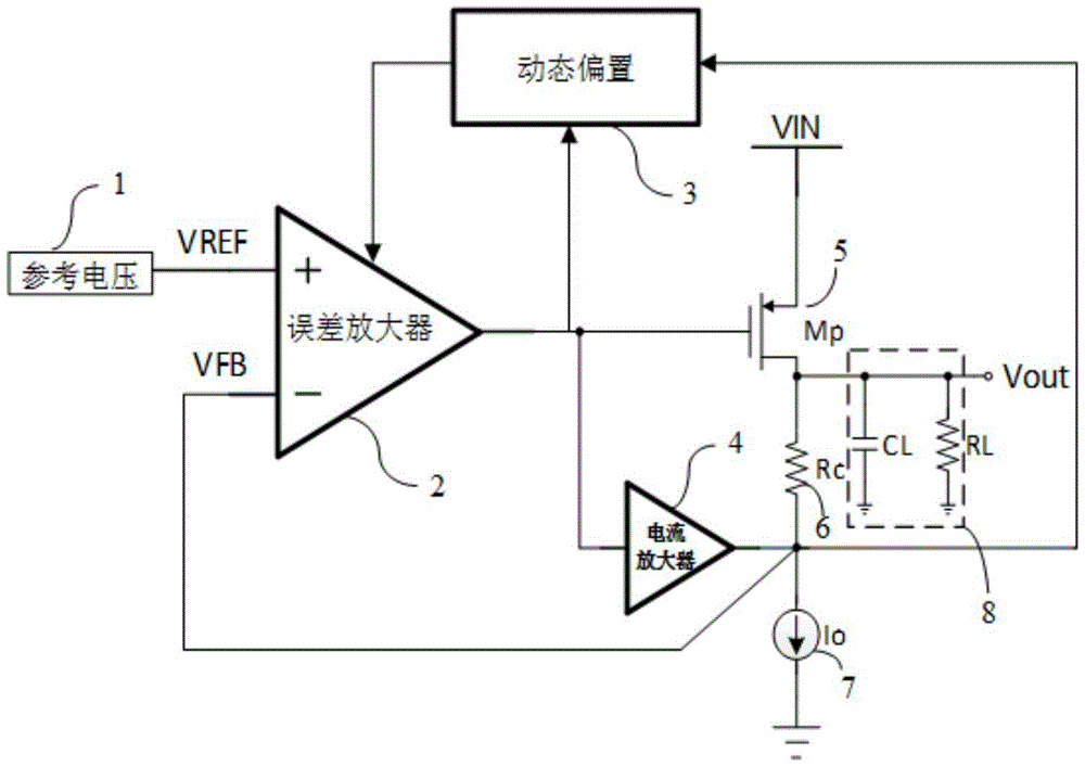
图3为动态偏置高PSRR低压差线性稳压器电路图。Figure 3 is a circuit diagram of a dynamic bias high PSRR low dropout linear regulator.
图4为实施例1的电路图。FIG. 4 is a circuit diagram of
图5为实施例2的电路图。FIG. 5 is a circuit diagram of
具体实施方式detailed description
如图3所示,本发明的动态偏置高PSRR低压差线性稳压器包括:参考电压单元1、误差放大器单元2、动态偏置电路3、电流放大器单元4、PMOS功率管Mp单元5、电阻Rc单元6、第七电流源I70单元7和负载阻抗单元8。误差放大器的输出端接功率管Mp的栅极和电流放大器的输入,误差放大器的正端接参考电压VREF,误差放大器的负端接反馈电压VFB,所述PMOS功率管源极接电源电压VIN,漏极与电阻Rc的一端、负载阻抗的一端接输出电压Vout,所述负载阻抗的另一端接地,所述电阻Rc的另一端、第七电流源I70的一端、电流放大器的输出接电压VFB,所述第七电流源I70的另一端接地,所述动态偏置电路的输入接电压VFB,输出接误差放大器和功率管的栅极。As shown in Figure 3, the dynamic bias high PSRR low dropout linear regulator of the present invention comprises:
为方便对照附图理解,以下以图中的标记作为器件的简称,例如,MOS管M1简写为M1。For the convenience of understanding with reference to the accompanying drawings, the symbols in the drawings are used as abbreviations of the devices below, for example, the MOS transistor M1 is abbreviated as M1.
图4示出了第一个实施例,误差放大器单元2包括MOS管M0、M1、M2、M3、M4、M5、M6、M7、M8、M9,电阻R1、R2、Ro1,电流源I20。MOS管M0的栅极接参考电压,源极与MOS管M1的源极接MOS管M2的漏极,漏极接MOS管M3的源极和电阻R1的一端,所述MOS管M1的栅极接VFB,漏极接MOS管M4的源极和电阻R2的一端,所述电阻R1和电阻R2的另一端接电源VIN,所述MOS管M3、M4的栅极接vbp,M3的漏极接电阻Ro1的一端和MOS管M5的漏极、源极、MOS管M6的栅极,M4的漏极、电阻Ro1的另一端、M6的漏极接Vo1,所述MOS管M5、M6的源极分别接MOS管M7、M8的漏极,所述MOS管M2、M7、M8的源极接地,栅极接vbn,所述MOS管M9的栅极接Vo1,源极接地,漏极和电流源I20的一端接Vo2,所述电流源I20的另一端接VIN。4 shows the first embodiment, the
本发明的动态偏置电路单元3包括MOS管Mc、M10、M11、M12,电阻Rd,电容C以及电流源I30、I31、I32、I33。所述MOS管Mc的栅极、电流源I30的一端、电阻Rd的一端、MOS管M10的栅极接Vc,MOS管Mc的漏极、电阻Rd的另一端接Vo2,所述电流源I30的另一端接地,所述MOS管M10的漏极、MOS管M12的漏极、MOS管M11的栅极和漏极和电流源I32的一端接vbn,所述电流源I32的另一端接地,MOS管M10的源极接电流源I31的一端,所述电流源I31的另一端接VIN,所述MOS管M12的栅极接电容C的一端,源极接电流源I33的一端,所述电流源I33的另一端接VIN,所述电容C的另一端接VFB。The dynamic
本发明的电流放大器4的一种简单实现方式包括PMOS管mp1、电流源I40,其中MOS管mp1是功率管Mp按宽度缩小一定倍数的同类型PMOS管。所述PMOS管mp1的栅极接Vo2,源极接VIN,漏极与电流源I40的一端接VFB,所述电流源I40的另一端接地。A simple implementation of the
电流源I32为误差放大器的第一级提供静态偏置,(I20-I30)为第二级提供静态偏置,电流源I70为功率管提供静态偏置。当负载电流接近零时,电流源I70、I30、I32、I20都很小,Vo2接近VIN,Mp、Mc趋近关断,rout很大,输出点为主极点;此时Mc、M10未能打开,IMc、I31为零。Vo1和Vo2处极点频率相当并远远高于主极点频率,系统带宽内只有单一极点。随着负载电流增加,一条快通路和一条慢通路共同对偏置电流有动态影响。快通路:负载电流增加,由于有限环路带宽和Mp栅较大寄生电容原因Vo2尚未反应,则VFB下降ΔVFB,由电容的高通特性,ΔVFB快速经电容C耦合到M12栅级上,此时M12打开,I33叠加到Ibiasn。慢通路:负载电流增加,经环路反应到Vo2点,Mc打开,调整流过M9的电流,从而使ro2骤降,I31叠加到Ibiasn,IMc、Ibiasn、mp1管的漏电流随负载电流增加,故ro1、ro2、rout减小,gm1、gm2、Gmp增加,ro1的最大值被限制在Ro1的一半。ro1、ro2、rout分别是误差放大器第一级、第二级及功率极的输出阻抗,gm1、gm2、Gmp分别为各级跨导。所以,Pout向高频移动、Po1向高频移动的速度要落后于Po2被移到很高频率点上速度。当电流继续增加直到M10、M12完全打开:Ibiasn恒定,IMc继续增加,gm1、ro1不变、ro2减少且之后随电流增加而减少的速度变慢、rout减小到最小drop voltage后则不再减少。The current source I32 provides a static bias for the first stage of the error amplifier, (I20-I30) provides a static bias for the second stage, and the current source I70 provides a static bias for the power tube. When the load current is close to zero, the current sources I70, I30, I32, and I20 are very small, Vo2 is close to VIN, Mp, Mc are close to off, r out is very large, and the output point is the main pole; at this time, Mc and M10 cannot Open, IMc, I31 are zero. The pole frequencies at Vo1 and Vo2 are equal and much higher than the dominant pole frequency, and there is only a single pole within the system bandwidth. A fast path and a slow path together have a dynamic effect on the bias current as the load current increases. Fast path: The load current increases. Due to the limited loop bandwidth and the large parasitic capacitance of the Mp gate, Vo2 has not yet responded, and the VFB drops by ΔV FB . Due to the high-pass characteristics of the capacitor, ΔV FB is quickly coupled to the M12 gate through the capacitor C. When M12 is open, I33 is superimposed to Ibiasn. Slow path: The load current increases, the loop reacts to Vo2 point, Mc opens, adjusts the current flowing through M9, so that r o2 drops suddenly, I31 is superimposed on Ibiasn, and the leakage current of IMc, Ibiasn, and mp1 tubes increases with the load current , so r o1 , r o2 , r out decrease, g m1 , g m2 , G mp increase, and the maximum value of r o1 is limited to half of Ro1. r o1 , r o2 , and r out are the output impedances of the first stage, the second stage, and the power pole of the error amplifier respectively, and g m1 , g m2 , and G mp are the transconductances of each stage respectively. Therefore, the speed of Pout moving to high frequency and Po1 moving to high frequency lags behind the speed of Po2 being moved to a high frequency point. When the current continues to increase until M10 and M12 are fully opened: Ibiasn is constant, IMc continues to increase, g m1 and r o1 remain unchanged, r o2 decreases and then decreases with the increase of current, and r out decreases to the minimum drop voltage will no longer decrease.
图5为第二个实施例,和图4相比,其动态偏置电路增加了MOS管Md。所述MOS管Md的栅极与漏极接Vo2,源极接VIN。较图4结构而言,图5增加的MOS管Md作VIN的前馈通路,使得系统的高频段PSRR特性变得更好,同时,IMd随着负载电流的增加而增加,ro2和gm2变化速度更快,故Po2移动到高频的速度变快,防止由于Po2移动的较慢而使得系统带宽减小致使系统在中频段的电源抑制性能变差。FIG. 5 shows the second embodiment. Compared with FIG. 4, the dynamic bias circuit has an added MOS tube Md. The gate and drain of the MOS transistor Md are connected to Vo2, and the source is connected to VIN. Compared with the structure in Figure 4, the MOS transistor Md added in Figure 5 is used as the feedforward path of VIN, which makes the PSRR characteristics of the high-frequency band of the system better. At the same time, IMd increases with the increase of the load current, r o2 and g m2 The speed of change is faster, so the speed of Po2 moving to high frequency becomes faster, preventing the system's power supply suppression performance in the mid-frequency band from deteriorating due to the slow movement of Po2 and the reduction of the system bandwidth.
通过以上分析,负载变化时,系统的全部零极点跟随变化,使得系统在全负载范围具有较大的带宽并且维持稳定,这样就可以在较宽的频率保持较高的PSRR。Through the above analysis, when the load changes, all the poles and zeros of the system follow the change, so that the system has a larger bandwidth and remains stable in the full load range, so that a higher PSRR can be maintained at a wider frequency.
Claims (3)
Priority Applications (1)
| Application Number | Priority Date | Filing Date | Title |
|---|---|---|---|
| CN202110947240.2A CN113672019B (en) | 2021-08-18 | 2021-08-18 | Dynamic bias high PSRR low dropout regulator |
Applications Claiming Priority (1)
| Application Number | Priority Date | Filing Date | Title |
|---|---|---|---|
| CN202110947240.2A CN113672019B (en) | 2021-08-18 | 2021-08-18 | Dynamic bias high PSRR low dropout regulator |
Publications (2)
| Publication Number | Publication Date |
|---|---|
| CN113672019A CN113672019A (en) | 2021-11-19 |
| CN113672019B true CN113672019B (en) | 2022-12-06 |
Family
ID=78543537
Family Applications (1)
| Application Number | Title | Priority Date | Filing Date |
|---|---|---|---|
| CN202110947240.2A Active CN113672019B (en) | 2021-08-18 | 2021-08-18 | Dynamic bias high PSRR low dropout regulator |
Country Status (1)
| Country | Link |
|---|---|
| CN (1) | CN113672019B (en) |
Families Citing this family (4)
| Publication number | Priority date | Publication date | Assignee | Title |
|---|---|---|---|---|
| CN115079765B (en) * | 2022-08-23 | 2022-11-15 | 上海韬润半导体有限公司 | Linear voltage regulator and integrated circuit device including the same |
| CN115857617B (en) * | 2022-11-24 | 2026-05-01 | 佛山大学 | CAFVF-based anti-radiation self-bias low-dropout voltage regulator circuit |
| CN116560446B (en) * | 2023-06-25 | 2025-12-02 | 无锡鸿恩泰科技有限公司 | A fully integrated LDO circuit for high-current applications and its operation method |
| CN120386418B (en) * | 2025-05-23 | 2026-04-28 | 江苏鑫康微电子科技有限公司 | High power supply rejection ratio and low dropout linear regulator circuit with dynamic bias current |
Family Cites Families (15)
| Publication number | Priority date | Publication date | Assignee | Title |
|---|---|---|---|---|
| FR2881537B1 (en) * | 2005-01-28 | 2007-05-11 | Atmel Corp | STANDARD CMOS REGULATOR WITH LOW FLOW, HIGH PSRR, LOW NOISE WITH NEW DYNAMIC COMPENSATION |
| US7417416B2 (en) * | 2005-10-27 | 2008-08-26 | International Business Machines Corporation | Regulator with load tracking bias |
| CN101364119A (en) * | 2008-07-07 | 2009-02-11 | 武汉大学 | Wide Dynamic Range Low Dropout Linear Regulator |
| EP2533126B1 (en) * | 2011-05-25 | 2020-07-08 | Dialog Semiconductor GmbH | A low drop-out voltage regulator with dynamic voltage control |
| US9134743B2 (en) * | 2012-04-30 | 2015-09-15 | Infineon Technologies Austria Ag | Low-dropout voltage regulator |
| US9235222B2 (en) * | 2012-05-17 | 2016-01-12 | Rf Micro Devices, Inc. | Hybrid regulator with composite feedback |
| US9671803B2 (en) * | 2013-10-25 | 2017-06-06 | Fairchild Semiconductor Corporation | Low drop out supply asymmetric dynamic biasing |
| CN105700601B (en) * | 2014-11-24 | 2018-08-24 | 深圳市中兴微电子技术有限公司 | A kind of LDO linear voltage regulators |
| CN107797599B (en) * | 2017-10-31 | 2019-09-03 | 中国电子科技集团公司第五十八研究所 | LDO circuit with dynamic compensation and fast transient response |
| US10571945B2 (en) * | 2018-02-21 | 2020-02-25 | Atlazo, Inc. | Low power regulator circuits, systems and methods regarding the same |
| US11036247B1 (en) * | 2019-11-28 | 2021-06-15 | Shenzhen GOODIX Technology Co., Ltd. | Voltage regulator circuit with high power supply rejection ratio |
| CN111290460B (en) * | 2020-02-25 | 2021-08-06 | 电子科技大学 | A Low Dropout Linear Regulator with High Power Supply Rejection Ratio and Fast Transient Response |
| CN111522389B (en) * | 2020-04-01 | 2024-08-16 | 博流智能科技(南京)有限公司 | Wide-input low-dropout linear voltage stabilizing circuit |
| CN111880596B (en) * | 2020-07-07 | 2022-01-18 | 芯创智(北京)微电子有限公司 | Dynamic bias circuit applied to ultralow static current LDO |
| CN112947656B (en) * | 2021-01-27 | 2022-09-27 | 浙江大学 | Low quiescent current, off-chip capacitor LDO with dynamically optimized power supply rejection ratio |
-
2021
- 2021-08-18 CN CN202110947240.2A patent/CN113672019B/en active Active
Also Published As
| Publication number | Publication date |
|---|---|
| CN113672019A (en) | 2021-11-19 |
Similar Documents
| Publication | Publication Date | Title |
|---|---|---|
| TWI434166B (en) | Method and apparatus for overshoot and undershoot errors correction in analog low dropout regulators | |
| CN108776506B (en) | A High Stability Low Dropout Linear Regulator | |
| CN100495281C (en) | Low-voltage-difference voltage-stablizer | |
| KR101238296B1 (en) | Compensation technique providing stability over broad range of output capacitor values | |
| CN110837268B (en) | Two-stage low dropout linear regulator with low noise and high power supply rejection ratio | |
| CN111273724B (en) | Stability-compensated linear voltage regulator and design method thereof | |
| US20030102851A1 (en) | Low dropout voltage regulator with non-miller frequency compensation | |
| CN111176358B (en) | Low-power-consumption low-dropout linear voltage regulator | |
| CN101105696A (en) | Voltage buffer circuit for linear potentiostat | |
| CN113672019A (en) | Dynamic bias high PSRR low dropout regulator | |
| JPH07212185A (en) | Analog filter circuit | |
| KR20040066050A (en) | Regulated cascode structure for voltage regulators | |
| CN115542996B (en) | A low-dropout linear regulator with high power supply rejection ratio and its control method | |
| CN111290460B (en) | A Low Dropout Linear Regulator with High Power Supply Rejection Ratio and Fast Transient Response | |
| CN110320963A (en) | Low-dropout linear voltage-regulating circuit | |
| CN115097894A (en) | Push-pull type LDO (low dropout regulator) with high power supply rejection ratio and without off-chip capacitor | |
| CN107422774A (en) | LDO on a kind of piece of low pressure fast transient response | |
| CN116501116B (en) | A linear regulator with high power supply rejection ratio and a voltage regulation method. | |
| CN113467559A (en) | Adaptive dynamic zero compensation circuit applied to LDO (low dropout regulator) | |
| CN117111670A (en) | A compensation circuit and low dropout linear voltage regulator | |
| CN109194326B (en) | Circuit for improving power supply rejection ratio of linear stabilized power supply | |
| CN116225118B (en) | An LDO circuit based on PN complementary current-compensated power supply ripple feedforward | |
| CN116466785B (en) | LDO circuit with low noise and high PSR | |
| CN114326904A (en) | Linear voltage stabilizer | |
| CN118519488A (en) | A low-dropout linear regulator with wide bandwidth and high PSR and no external capacitor |
Legal Events
| Date | Code | Title | Description |
|---|---|---|---|
| PB01 | Publication | ||
| PB01 | Publication | ||
| SE01 | Entry into force of request for substantive examination | ||
| SE01 | Entry into force of request for substantive examination | ||
| CB02 | Change of applicant information |
Address after: No. 2201 and 2301, floor 22-23, building 1, No. 1800, middle section of Yizhou Avenue, high tech Zone, China (Sichuan) pilot Free Trade Zone, Chengdu, Sichuan 610041 Applicant after: Chengdu Hua Microelectronics Technology Co.,Ltd. Address before: 610000 22 / F, building 1, No. 1800, middle section of Yizhou Avenue, hi tech Zone, Chengdu City, Sichuan Province Applicant before: CHENGDU SINO MICROELECTRONICS TECHNOLOGY Co.,Ltd. |
|
| CB02 | Change of applicant information | ||
| GR01 | Patent grant | ||
| GR01 | Patent grant |