Detailed Description
(1) Photosensitive body
The photoreceptor of the present invention comprises at least a laminated photosensitive layer in which a charge generation layer containing a charge generation substance and a charge transport layer containing a charge transport substance are laminated in this order on a substrate,
the charge generating substance is oxytitanium phthalocyanine having at least diffraction peaks at bragg angles (2 theta + -0.2 DEG) of 7.3 DEG, 9.4 DEG, 11.6 DEG, 24.2 DEG and 27.3 DEG in an X-ray diffraction spectrum using CuK alpha rays,
the laminated photosensitive layer is characterized by having a maximum absorption (lambda) at a wavelength of 800-850 nm in a spectral absorption spectrummax) And the minimum absorbance of the light with a wavelength of 400-800 nm is taken as 0Peak intensity at wavelength 780nm (Abs) at the time of correction780nm) And peak intensity (Abs) at wavelength 860nm860nm) Abs ratio of (A)860nm/Abs780nmIs 0.6 to 1.2 inclusive.
When the photosensitive layer of the photoreceptor of the present invention has the spectral absorption spectrum described above, λ max of the phthalocyanine dye has strong absorption on the long wavelength side, which indicates that the intermolecular interaction of the phthalocyanine dye is strong.
When the photosensitive layer is exposed to external light, an amount corresponding to absorbed light energy is activated into an excited state, and the more stable the excited state, the greater the influence on the image. Therefore, it is considered how a structure which can be quickly deactivated from the excited state to the ground state can be formed, but the light fastness of the photosensitive layer is affected.
The photoreceptor of the present invention is presumed to have the spectral absorption spectrum described above, and charges in an excited state exposed to external light move between pi-pi bonds of the phthalocyanine dye, and are easily and rapidly deactivated in a ground state, resulting in formation of a photosensitive layer having good light resistance.
That is, the photoreceptor of the present invention is characterized in that the laminated photosensitive layer containing a specific oxytitanium phthalocyanine as a charge generating substance on the substrate has a specific spectral absorption spectrum.
First, the oxytitanium phthalocyanine and the laminated photosensitive layer (hereinafter, also referred to as "photosensitive layer") will be described, and then the photoreceptor and the image forming apparatus including the photoreceptor will be described.
< oxytitanium phthalocyanine >
In the present invention, oxytitanium phthalocyanine used as a charge generating substance has at least diffraction peaks at bragg angles (2 θ ± 0.2 °) of 7.3 °, 9.4 °, 11.6 °, 24.2 ° and 27.3 ° in an X-ray diffraction spectrum using CuK α line.
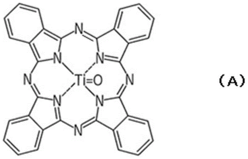
The oxytitanium phthalocyanine is represented by the following formula (A).
[ solution 1]
The oxytitanium phthalocyanine represented by the formula (A) can be produced by a known synthesis method described in, for example, Frank H, Moser and Arthur L.Thomas, "Phthalocyanine Componed", Reinhold Publishing Corporation (New York) in 1963, Japanese patent application laid-open Nos. 6-293769, 2003-18534, 7-271073 and Frank H.
The present inventors have confirmed that the excellent effects of the present invention can be obtained regardless of the starting material and method of synthesis as long as the oxytitanium phthalocyanine having the above-described X-ray diffraction spectrum characteristics is used. However, as described later, a halogen such as chlorine contained in oxytitanium phthalocyanine may adversely affect the charging performance of the photoreceptor, and the oxytitanium phthalocyanine is preferably derived from a raw material containing no halogen such as chlorine.
The following exemplifies the synthesis method. However, the following synthetic route is an example, and is not limited thereto.
A titanium alkoxide such as phthalonitrile and titanium tetrabutoxide is reacted in the presence of urea while stirring at 150 ℃ for at least 5 hours or more. After the reaction is finished, the obtained product is filtered to obtain the generated oxytitanium phthalocyanine. Using alcohols such as methanol, ethanol, n-propanol, butanol; chlorine-based hydrocarbons such as dichloroethane and chloroform; ethers such as dimethyl ether, diethyl ether and tetrahydrofuran; the obtained product is washed with a solvent such as ketone, e.g., acetone or methyl ethyl ketone, to obtain oxytitanium phthalocyanine. Since oxytitanium phthalocyanine is insoluble in these solvents and impurities adhering to the oxytitanium phthalocyanine are dissolved, the residue of impurities can be reduced to the limit by repeating washing.
Furthermore, after dichlorotitanium phthalocyanine is synthesized by heating and melting phthalonitrile and titanium tetrachloride or by heating reaction in an appropriate solvent such as α -chloronaphthalene, oxytitanium phthalocyanine is obtained by hydrolysis with alkali or water.
Further, oxytitanium phthalocyanine is obtained by subjecting titanium tetraalkoxide such as isoindoline and titanium tetrabutoxide to a heating reaction in an appropriate solvent such as N-methylpyrrolidone. The oxytitanium phthalocyanine may contain a phthalocyanine derivative in which a hydrogen atom of a benzene ring of the phthalocyanine derivative is substituted with a substituent such as chlorine, fluorine, nitro, cyano, or sulfo.
The thus-obtained oxytitanium phthalocyanine is treated with an organic solvent immiscible with water such as dichloroethane in the presence of water, whereby a crystalline oxytitanium phthalocyanine used as a charge generating substance in the present invention can be obtained.
As a method of treating the crystal (crystal conversion method), for example: a method of swelling oxytitanium phthalocyanine in water and treating it with an organic solvent, a method of adding water to an organic solvent without performing a swelling treatment and charging oxytitanium phthalocyanine powder therein, and the like.
As a method for swelling oxytitanium phthalocyanine in water, for example, oxytitanium phthalocyanine is dissolved in concentrated sulfuric acid 10 to 30 times in volume, and when insoluble substances appear, the insoluble substances are removed by filtration or the like, and precipitated in water after cooling. Next, the obtained oxytitanium phthalocyanine is filtered with ion-exchanged water or the like to remove an acid, and the washing operation is repeated until the obtained product is neutral to obtain a wet cake (also referred to as "wet paste").
When the oxytitanium phthalocyanine is swollen in water, a known stirring and dispersing device such as a homomixer, a paint mixer, a ball mill, a sand mill or the like can be used.
Thus, amorphous oxytitanium phthalocyanine (low-crystalline oxytitanium phthalocyanine) can be converted into oxytitanium phthalocyanine crystals having a specific diffraction peak.
More specifically, a crystal conversion method of oxytitanium phthalocyanine will be described.
Specifically, the amorphous oxytitanium phthalocyanine (low-crystalline titanyl phthalocyanine) in the wet cake form is not dried, and the intended crystal form can be obtained by mixing and stirring in the presence of water and an organic solvent.
The organic solvent used herein may be tetrahydrofuran alone, or a mixed solvent with toluene, methylene chloride, carbon disulfide, o-dichlorobenzene, and one selected from 1, 1, 2-trichloroethane, as long as the desired crystal form is obtained.
Further, the oxytitanium phthalocyanine of the present invention can be obtained by stirring the amorphous oxytitanium phthalocyanine of the wet cake for a sufficient period of time or grinding the amorphous oxytitanium phthalocyanine by mechanical strain.
Examples of the apparatus used for the treatment include a homogenizing mixer, a dispersing mixer, a disperser, a stirrer, a ball mill, a sand mill, an attritor, an ultrasonic dispersing apparatus, and the like, in addition to a general stirring apparatus. After the treatment, the extract may be filtered by a known method, washed with methanol, ethanol, water or the like, and separated.
In the present invention, the oxytitanium phthalocyanine used as the charge generating substance preferably has an average particle diameter D (50%) of 0.15 to 0.3. mu.m.
For example, when a coating liquid for forming a charge generation layer, which will be described later, is dispersed, oxytitanium phthalocyanine is pulverized (crushed) and the average particle diameter thereof is less than 0.15 μm, the generation efficiency of the carrier is lowered, and the sensitivity of the photoreceptor tends to be deteriorated, and further, since the occupancy ratio of the dye during dispersion is too high, coating defects are easily generated during film formation, and stable charges are hardly generated during long-term use. On the other hand, if the average particle size exceeds 0.3 μm, the particle size distribution tends to deteriorate during long-term storage, and coating defects tend to occur during film formation of the charge generation layer.
More preferably, the oxytitanium phthalocyanine has an average particle diameter of 0.18 to 0.28. mu.m.
The method for measuring the average particle diameter is described in detail in examples.
< photosensitive layer >
The photosensitive layer of the photoreceptor of the present invention has a maximum absorption (. lamda.) at a wavelength of 800 to 850nm in a spectral absorption spectrummax) And a peak intensity (Abs) at a wavelength of 780nm when the peak intensity is corrected with the minimum absorbance at a wavelength of 400 to 800nm as 0780nm) And peak intensity (Abs) at wavelength 860nm860nm) Abs ratio of (A)860nm/Abs780nmIs 0.6 to 1.2 inclusive.
When the maximum absorption (. lamda.max) is less than the wavelength of 800nm, light resistance and reduction in charging due to repeated use may be deteriorated. On the other hand, even if the maximum absorption (. lamda.max) exceeds 850nm, the light resistance is sometimes lowered, and therefore, it is preferable to fall within the range specified in the present invention.
The preferred wavelength of maximum absorption is 800 to 830 nm.
Further, if the ratio of the peak intensity is less than 0.6, the light resistance is particularly poor, and it is necessary to introduce an ultraviolet absorber into the Charge Transport Layer (CTL). This is considered to be because the maximum absorption (. lamda.max) is shifted to a low wavelength and the peak intensity ratio becomes small, so that the interaction between oxytitanium phthalocyanines is weakened, and when exposed to strong external light, residual carriers generated in the charge generation layer upon repeated electrical fatigue exposure are not inactivated and remain. On the contrary, if the ratio of the peak intensities exceeds 1.2, the maximum absorption (λ max) shifts to a low wavelength, and the repeated VL (surface potential) rise becomes large.
The ratio of the peak intensities is preferably 0.75 to 1.
The spectral absorption spectrum (absorbance) of the photosensitive layer can be controlled by adjusting the conditions (dispersion method, dispersion time, medium diameter, medium amount, and material of the medium) for synthesizing the charge generating substance and dispersing the coating liquid for forming the charge generating layer.
In the synthetic route of the charge generating substance, it is important to reduce impurities as much as possible. For example, it is important to lower the sulfate ion concentration in the deacidification step in a washing state closer to ph7.0, and when impurities remain in this step, it is difficult to adjust the maximum absorption (λ max) of the absorption spectrum to the long wavelength side. The presence of impurities leads to a crystal structure in which the interaction between phthalocyanines is weak, and therefore, it is important to maintain stable electrical characteristics over a long period of use.
Further, the amount of impurities remaining can be reduced by selecting the crystallization conditions and the crystallization solvent in the crystallization step of oxytitanium phthalocyanine. The addition of toluene as a crystallization solvent can enhance the cleaning of impurities, but the addition of a high boiling point solvent increases the amount of solvent remaining in the crystals, and may affect the properties thereof. It is preferable to suppress impurities in the synthesis step and reduce the residual solvent.
On the other hand, the adjustment of the allocation condition by the dispersion may be performed.
The distribution is performed by using a crushing device with spherical media with the media diameter of 0.1-3.0 mm, preferably 0.1-2.0 mm. When the medium diameter is larger than 2.0mm, the pulverization efficiency tends to be lowered. Therefore, the maximum absorption (. lamda.max) cannot be adjusted within the range specified in the present invention, or the phthalocyanine occupies an excessively large proportion due to the prolonged dispersion time, and there is no problem such as deterioration in the characteristics, reduction in the particle diameter, and generation of aggregates.
Further, the pulverization efficiency also varies depending on the material of the medium, and the optimum conditions are influenced by the phthalocyanine dye, so that it is necessary to select optimum dispersion conditions for each material. If the maximum absorption wavelength is within the predetermined range of the present invention, the adjustment from the synthesis step, the adjustment from the distribution condition, and the like are not particularly limited, and the effects described in the present invention can be maintained.
< electrophotographic photoreceptor >
The photoreceptor of the present invention includes at least a laminated photosensitive layer in which a charge generation layer containing a charge generation substance and a charge transport layer containing a charge transport substance are sequentially laminated on a substrate.
The photoreceptor of the present invention will be described below with reference to the drawings, but the present invention is not limited thereto.
Fig. 2 is a schematic cross-sectional view showing the configuration of a main part of a photoreceptor (laminated photoreceptor) F01 according to the present invention.
The laminated photoreceptor F01 includes a photosensitive layer in which a primer layer F21, a charge generation layer F22 containing a charge generation substance, and a charge transport layer F23 containing a charge transport substance are sequentially laminated on a substrate F1. In the figure, Fa denotes the photoreceptor surface.
< substrate F1>
The substrate (also referred to as "conductive substrate" or "conductive support") has a function as an electrode of the photoreceptor and a function as a support member, and the constituent material thereof is not particularly limited as long as it is a material used in the art.
Specific examples thereof include metal materials such as aluminum, aluminum alloys, copper, zinc, stainless steel, and titanium; and polymer materials such as polyethylene terephthalate, nylon, and polystyrene, hard paper, glass, and the like, the surfaces of which are laminated with a metal foil, subjected to a metal vapor deposition treatment, or subjected to vapor deposition or coating with a layer of a conductive polymer, a conductive compound such as tin oxide, indium oxide, and the like. Among them, aluminum is preferable in terms of ease of processing, and aluminum alloys such as JIS3003 series, JIS5000 series, and JIS6000 series are particularly preferable.
The shape of the conductive support is not limited to the cylindrical shape (drum shape) as shown in fig. 3, and may be a sheet shape, a cylindrical shape, an annular band shape, or the like.
The surface of the conductive support may be subjected to an anodic oxide film treatment, a surface treatment with chemicals, hot water, or the like, a coloring treatment, or a diffuse reflection treatment such as roughening of the surface, as necessary, in order to prevent interference fringes due to laser light, within a range that does not affect the image quality.
< undercoat layer F21>
The photoreceptor of the present invention preferably includes an undercoat layer (also referred to as an "intermediate layer") between the substrate and the laminated photosensitive layer.
In general, the undercoat layer uniformly coats the surface of the substrate to improve the film-forming property of the laminated photosensitive layer, suppress the peeling of the photosensitive layer from the conductive support, and improve the adhesion between the substrate and the photosensitive layer. Specifically, it is possible to prevent charge from being injected from the substrate into the photosensitive layer, prevent the chargeability of the photosensitive layer from being lowered, and prevent fogging (so-called blackening) of an image.
The undercoat layer can be formed, for example, by dissolving or dispersing a binder resin in an appropriate solvent to prepare a coating liquid for the undercoat layer, applying the coating liquid to the surface of the substrate, and drying to remove the organic solvent.
Examples of the binder resin include acetal resin, polyamide resin, polyurethane resin, polyester resin, acrylic resin, epoxy resin, phenol resin, melanin resin, and polyurethane resin. The binder resin requires the following characteristics: does not dissolve, swell, or the like a solvent used in forming the photoreceptor layer on the undercoat layer; excellent adhesion to the conductive support; among the binder resins, polyamide resins are preferred because of their flexibility, and polyamide resins containing an alcohol-soluble nylon resin and a piperazine compound are particularly preferred.
Examples of the alcohol-soluble nylon resin include those obtained by chemically modifying nylon such as nylon 6, nylon 66, nylon 610, nylon 11, nylon 12, and other homo-or co-polymerized nylon, and N-alkoxymethyl-modified nylon.
Further, a curing agent for crosslinking the binder resin may be used as the cured film. As the curing agent, blocked isocyanates are preferable from the viewpoint of storage stability and electrical characteristics of the coating liquid.
Examples of the solvent include lower alcohols such as water, methanol, ethanol, n-propanol, isopropanol, n-butanol, 2-butanol, and isobutanol; ketones such as acetone, cyclohexanone, and 2-butanone; ethers such as tetrahydrofuran, dioxane, ethylene glycol, and diethyl ether; halogenated hydrocarbons such as methylene chloride and vinyl chloride. These solvents may be used alone or in combination of two or more selected from the solubility of the binder resin, the surface smoothness of the undercoat layer, and the like.
Among these solvents, non-halogen organic solvents can be suitably used in consideration of global environment.
The coating liquid for forming an undercoat layer may contain metal oxide particles. The metal oxide particles can easily adjust the volume resistance value of the undercoat layer, can further suppress injection of charges into the charge generation layer, and can maintain the electrical characteristics of the photoreceptor in various environments.
Examples of the material that can be used for the metal oxide particles include titanium oxide, aluminum hydroxide, and tin oxide.
The ratio (A/B) of the total mass A of the binder resin and the metal oxide particles to the mass B of the solvent in the coating liquid for forming the undercoat layer is, for example, preferably about 1/99 to 30/70, and particularly preferably about 2/98 to 40/60.
The ratio (C/D) of the mass C of the binder resin to the mass D of the metal oxide particles is, for example, preferably about 90/10 to 1/99, and particularly preferably about 70/30 to 5/95.
The method of applying the coating liquid for the undercoat layer may be appropriately selected from the most suitable methods in consideration of the physical properties of the coating liquid, productivity, and the like, and examples thereof include a spray coating method, a bar coating method, a roll coating method, a blade coating method, a ring coating method, a dip coating method, and the like.
Among them, the dip coating method is a method in which a substrate is dipped in a coating bath filled with a coating liquid and then pulled up at a constant speed or a speed that changes gradually, and thus a layer is formed on the surface of the substrate, which is relatively simple and advantageous in terms of productivity and cost, and thus can be suitably used for manufacturing a photoreceptor. In the apparatus used in the dip coating method, a coating liquid dispersing apparatus typified by an ultrasonic wave generating apparatus may be provided in order to stabilize the dispersibility of the coating liquid.
The solvent in the coating film can be removed by natural drying, or can be forcibly removed by heating.
The temperature in such a drying step is not particularly limited as long as it is a temperature at which the solvent used can be removed, but is preferably about 50 to 140 ℃, and more preferably about 80 to 130 ℃.
When the drying temperature is less than 50 ℃, the drying time may become long, and the solvent may not be sufficiently evaporated and may remain in the photoreceptor layer. Further, if the drying temperature exceeds about 140 ℃, the electrical characteristics of the photoreceptor upon repeated use deteriorate, and the resulting image deteriorates.
Such temperature conditions are common not only in the undercoat layer, but also in the layer formation of a photosensitive layer or the like described later and other processes.
The thickness of the primer layer is not particularly limited, but is preferably 0.01 to 20 μm, and more preferably 0.05 to 10 μm.
When the film thickness of the undercoat layer is less than 0.01 μm, sufficient effects of the blocking property of electron injection from the conductive substrate side and the countermeasure against interference fringes due to light scattering may not be obtained. On the other hand, if the film thickness of the undercoat layer exceeds 20 μm, the sensitivity change during continuous printing becomes large, and further the change in image density becomes large.
< Charge generating layer F22>
The charge generating layer has a function of generating charges by absorbing light irradiated from a light emitting device such as a beam of a semiconductor laser in an electrophotographic device such as an image forming apparatus, and contains a charge generating substance as a main component and may contain a binder resin or an additive as needed.
The above-mentioned oxytitanium phthalocyanine is used as the charge generating substance, and other charge generating substances known in the art may be used in combination as long as the effect is not impaired, and the photoreceptor of the present invention is improved in characteristics according to the content of oxytitanium phthalocyanine, so that the content is preferably at least 80% as large as possible.
As a method for forming the charge generating layer, a method is preferred in which a charge generating substance is dispersed in a binder resin solution obtained by mixing a binder resin with a solvent by a conventionally known method, and a coating liquid for the charge generating layer is applied to the undercoat layer. This method will be explained below.
Examples of the other charge generating substance include other metal phthalocyanines such as α -type, β -type, Y-type, and amorphous oxytitanium phthalocyanine and gallium having a crystal form different from that of the oxytitanium phthalocyanine, monoazo dyes, azo dyes such as bisazo dyes and trisazo dyes, indigo dyes such as indigo and thioindigo, perylene dyes such as perylene imide and perylene anhydride, polycyclic quinone dyes such as anthraquinone and pyrenequinone, phthalocyanine dyes such as metal phthalocyanines and metal-free phthalocyanines such as oxytitanium phthalocyanine, squarylium pigments, pyrylium salts, Thiopyrylium salts, organic conductive materials such as triphenylmethane pigments, and inorganic photoconductive materials such as selenium and amorphous silicon, and substances having appropriate exposure sensitivity can be selected and used as appropriate.
The binder resin is not particularly limited, and a resin having adhesive properties used in the technical field and the binder resins exemplified in the primer layer can be used, and a binder resin having excellent compatibility with a charge generating substance is preferable.
Specifically, there may be mentioned polyester, polystyrene, polyurethane, phenol resin, alkyd resin, melamine resin, epoxy resin, silicone resin, acrylic resin, methacrylic resin, polycarbonate, polyarylate, phenoxy resin, polyvinyl butyral (PVB), polyvinyl formal, and copolymer resins containing two or more of the repeating units constituting these resins. Examples of the copolymer resin include insulating resins such as vinyl chloride-vinyl acetate copolymer resin, vinyl chloride-vinyl acetate-maleic anhydride copolymer resin, and acrylonitrile-styrene copolymer resin. These binder resins may be used singly or in combination of two or more.
In the present invention, the binder resin is preferably a resin obtained by acetalization of 2 or more kinds of aldehydes with polyvinyl alcohol, and has a weight average molecular weight of 6 to 20 ten thousand.
When the weight average molecular weight is less than 6 ten thousand, the oxytitanium phthalocyanine of the present invention tends to be poor in dispersibility, to cause a problem in film-forming property, and to cause a problem in dispersion stability during long-term storage. On the other hand, if the weight average molecular weight exceeds 20 ten thousand, the viscosity of the dispersion coating liquid increases, and the crystal system of oxytitanium phthalocyanine collapses.
More preferably, the weight average molecular weight is in the range of 8 to 12 ten thousand.
The weight average molecular weight can be measured by a known method.
Examples of the solvent include: halogenated hydrocarbons such as dichloromethane and dichloroethane; ketones such as acetone, methyl ethyl ketone, and cyclohexanone; esters such as ethyl acetate and butyl acetate; ethers such as Tetrahydrofuran (THF) and dioxane; alkyl ethers of ethylene glycol such as 1, 2-dimethoxyethane; aromatic hydrocarbons such as benzene, toluene, and xylene; aprotic polar solvents such as N, N-dimethylformamide and N, N-dimethylacetamide. These solvents may be used singly or in combination of two or more.
Among these solvents, non-halogen organic solvents can be suitably used in consideration of global environment.
Similarly to the undercoat layer, a dispersing machine such as a paint shaker, a ball mill, or a sand mill may be used to dissolve or disperse the charge generating substance in the binder resin solution. In this case, it is preferable to appropriately set the dispersion conditions so that impurities are not mixed into the coating liquid due to abrasion or the like from the container and members constituting the dispersion machine.
The ratio (E/F) of the mass E of the charge generating substance to the mass F of the binder resin is, for example, preferably about 80/20 to 55/45.
If the ratio (E/F) exceeds 80/20, that is, if the mass E of the charge generating substance becomes large, the charge generating substance becomes excessive and the dispersion stability in the binder resin deteriorates. On the other hand, if the ratio (E/F) is less than 55/45, i.e., the mass E of the charge generating substance becomes small, the charge generating efficiency decreases and the sensitivity deteriorates.
More preferably, the ratio is about 60/40 to 70/30.
The thickness of the charge generation layer is not particularly limited, but is preferably 0.05 to 5 μm, and more preferably 0.1 to 1 μm.
When the film thickness of the charge generation layer is less than 0.05 μm, the efficiency of light absorption decreases, and the sensitivity of the photoreceptor decreases. On the other hand, if the film thickness of the charge generation layer exceeds 5 μm, the sensitivity of the photoreceptor decreases at a stage where the charge transfer in the charge generation layer becomes a rate-limiting step in the process of eliminating the charge on the surface of the photoreceptor layer.
< Charge transport layer F23>
The charge transport layer has a function of receiving charges generated by the charge generating substance and transporting the charges to the surface (Fa in fig. 2) of the photoreceptor, contains a charge transport substance and a binder resin, and contains an additive as necessary.
The charge transport material is not particularly limited, and a compound used in the art can be used.
Specific examples thereof include carbazole derivatives, pyrene derivatives, oxazole derivatives, oxadiazole derivatives, thiazole derivatives, thiadiazole derivatives, triazole derivatives, imidazole derivatives, imidazolidinone derivatives, imidazoline derivatives, bisimidazoline derivatives, styryl compounds, hydrazone compounds, polycyclic compounds, indole derivatives, pyrazoline derivatives, oxazolone derivatives, benzimidazole derivatives, quinazoline derivatives, benzofuran derivatives, acridine derivatives, phenazine derivatives, aminostilbene derivatives, triarylamine derivatives, phenylenediamine derivatives, stilbene derivatives, diphenylamine derivatives, dibenzozine derivatives, and polymers having a group derived from these compounds in the main or side chain (poly-N-vinylcarbazole, poly-1-vinylpyrene, ethylcarbazole-formaldehyde resin, oxadiazole derivatives, thiazole derivatives, thiadiazole derivatives, triazole derivatives, imidazole derivatives, imidazolone derivatives, imidazoline derivatives, bisimidazoline derivatives, acridine derivatives, phenazine derivatives, triarylamine derivatives, phenylenediamine derivatives, stilbene derivatives, diphenylamine derivatives, dibenzozine derivatives, and polymers having a group derived from these compounds in the main or side chain (poly-N-vinylcarbazole, poly-1-vinylpyrene, ethylcarbazole-formaldehyde resin, and oxadiazole derivatives, Triphenylmethane polymers, poly-9-vinyl anthracene polymers), polysilanes, and the like. These charge transport materials may be used singly or in combination of two or more.
Among these charge transport materials, the triene amine dimer compound represented by the general formula (1) and the stilbene derivative represented by the general formula (2) described below are particularly preferable.
The triene amine dimer compound is represented by the general formula (1):
[ solution 2]
In the formula, Ar1And Ar2Are identical or different, optionally substituted alkynyl or optionally substituted heterocycle-derived 2-valent radicals, Ar3And Ar4Is the same or different and may have a substituted aryl group or may have a substituted heterocyclic group, R1And R2The same or different is an alkyl group, m and n are integers of 1 to 4, a and b are the same or different and are a hydrogen atom, a halogen atom, an alkyl group, a fluoroalkyl group, an alkoxy group or an amino group which may have a substituent, and in the case where m or n is 2 or more, two a or b bonded to adjacent positions are combined with each other to form a methylenedioxy group, an ethylenedioxy group, a tetramethylene group or a butadienyl group.
Examples of the triene amine dimer compound of the general formula (1) include compounds described in japanese patent No. 4604083, and can be synthesized by the method described in the above publication.
Specifically, Ar used in examples is1And Ar2Is p-phenylene, Ar3And Ar4Is phenyl, R1And R2A triene amine dimer compound (triene amine compound) of the formula (a) wherein a and b are methyl groups, the number of atoms n and m is 1.
The stilbene derivative is represented by the general formula (2):
[ solution 3]
In the formula, R1、R2、R5And R6The same or different alkyl, alkoxy, aryl, aralkyl or halogen atoms, m, n, p and q are the same or different and are integers of 0-3, wherein R is1And R2When they are the same group, m and n are different integers, and R is5And R6When the radicals are identical, p and q are different integers, R3And R4The same or different, is a hydrogen atom or an alkyl group.
Examples of stilbene derivatives of the general formula (2) include compounds described in Japanese patent No. 3272257, and these stilbene derivatives can be synthesized by the methods described in these publications.
Specifically, R used in examples1、R2、R5And R6Is methyl, R3And R4Stilbene derivatives (stilbene compounds) of formula (b) which are hydrogen atoms, the number of atoms n and p being 1, the number of atoms m and q being 1.
For the substituent R of the general formula (2)1、R2、R5And R6The description is given.
Examples of the alkyl group include alkyl groups having 1 to 6 carbon atoms such as a methyl group, an ethyl group, a n-propyl group, an isopropyl group, a n-butyl group, an isobutyl group, a sec-butyl group, a tert-butyl group, a n-pentyl group, and a n-hexyl group.
Examples of the alkoxy group include alkoxy groups having 1 to 6 carbon atoms such as a methoxy group, an ethoxy group, a n-propoxy group, an isopropoxy group, a tert-butoxy group, a n-pentoxy group, and a n-hexoxy group.
Examples of the aryl group include aryl groups such as phenyl, naphthyl, anthryl, phenanthryl, fluorenyl, biphenyl, and ortho-terphenyl.
Examples of the aralkyl group include aralkyl groups such as a benzyl group, a phenethyl group, a benzhydryl group, and a trityl group.
Examples of the halogen atom include fluorine, chlorine, bromine, and iodine.
Substituent R1、R2、R5And R6When the number of atoms m, n, p and q in (A) is 2 or more, the substituents may be different from each other, for example, the substituent R1When the number m of atoms in (b) is 2, the same benzene ring may be substituted with different groups such as methyl and ethyl groups and methyl and ethoxy groups.
As substituent R of the general formula (1)3And R4Examples of the alkyl group of (b) include alkyl groups having 1 to 3 carbon atoms such as a methyl group, an ethyl group, an n-propyl group, and an isopropyl group.
As a method for forming the charge transport layer, a method in which a charge transport material is dispersed in a binder resin solution obtained by mixing a binder resin in a solvent by a conventionally known method and a coating liquid for the charge transport layer is applied to the charge generation layer is preferable. This method will be explained below.
The binder resin is not particularly limited, and a resin having adhesive properties used in the art can be used, and a resin having excellent compatibility with a charge transport material is preferable.
Specifically, there may be mentioned vinyl polymer resins such as polymethyl methacrylate, polystyrene and polyvinyl chloride, copolymer resins thereof, resins such as polycarbonate, polyester carbonate, polysulfone, phenoxy resin, epoxy resin, silicone resin, polyarylate, polyamide, polyether, polyurethane, polyacrylamide, phenol resin and polyphenylene ether, and thermosetting resins obtained by partially crosslinking these resins. These binder resins may be used singly or in combination of two or more.
Wherein the polystyrene, polycarbonate, polyarylate and polyphenylene ether have a volume resistance value of 1013Since Ω or more is excellent in electrical insulation properties and also excellent in film forming properties, potential characteristics, etc., polycarbonate is particularly preferable.
Examples of the solvent include: aromatic hydrocarbons such as benzene, toluene, xylene, and monochlorobenzene; halogenated hydrocarbons such as dichloromethane and dichloroethane; ethers such as tetrahydrofuran, dioxane, and dimethoxymethyl ether; and aprotic polar solvents such as N, N-dimethylformamide. Further, a solvent such as alcohol, acetonitrile or methyl ethyl ketone may be added as necessary. These solvents may be used singly or in combination of two or more.
Among these solvents, non-halogen organic solvents can be suitably used in consideration of global environment.
The charge transport layer may contain an additive within a range not to hinder the effects of the present invention.
Examples of the additive include ultraviolet absorbers for improving light resistance, and specifically, the perinone dyes used in examples.
However, the addition of the additive to the charge transport layer forms a trap for charge transport, adversely affects the characteristics of the photoreceptor, and is about 1 to 10 parts by mass relative to the charge transport material.
The ratio (G/H) of the mass G of the charge transport material to the mass H of the binder resin is, for example, preferably about 10/12 to 10/30.
The film thickness of the charge transport layer is not particularly limited, but is preferably 5 to 50 μm, and more preferably about 10 to 40 μm.
If the film thickness of the charge transport layer is less than 5 μm, the charge retention ability of the surface of the photoreceptor is lowered. On the other hand, when the film thickness of the charge transport layer exceeds 50 μm, the resolution of the photoreceptor is lowered.
(2) Image forming apparatus 100
An image forming apparatus of the present invention includes at least: the photoreceptor of the present invention; a charging unit for charging the photoreceptor; an exposure unit that exposes the charged photoreceptor to form an electrostatic latent image; a developing unit that develops the electrostatic latent image formed by the exposure to form a toner image (visualized); a transfer unit that transfers the toner image formed by the development onto a recording medium; a fixing unit that fixes the transferred toner image on a recording medium to form an image; a cleaning unit for removing and recovering the residual toner on the photoreceptor; and a charge removing unit for removing the surface charges remaining on the photoreceptor.
Hereinafter, an image forming apparatus and an operation thereof according to the present invention will be described with reference to the drawings, but the present invention is not limited to the following description.
Fig. 3 is a schematic side view showing a configuration of a main part of image forming apparatus 100 according to the present invention.
The image forming apparatus (laser printer) 100 of fig. 3 includes the photoreceptor 1 (corresponding to F01 of fig. 2) of the present invention, an exposure unit (semiconductor laser) 31, a charging unit (charger) 32, a developing unit (developer) 33, a transfer unit (transfer charger) 34, a conveying belt (not shown), a fixing unit (fixer) 35, and a cleaning unit (cleaner) 36. Reference numeral 51 denotes a recording medium (recording paper or transfer paper).
Photoreceptor 1 is rotatably supported by the main body of image forming apparatus 100, and is driven by a drive unit, not shown, to rotate in the direction of arrow 41 around rotation axis 44. The driving unit includes, for example, a motor and a reduction gear, and transmits its driving force to a conductive support body constituting a core of the photoreceptor 1, thereby driving the photoreceptor 1 to rotate at a predetermined circumferential speed. A charging unit (charger) 32, an exposure unit 31, a developing unit (developer) 33, a transfer unit (transfer charger) 34, and a cleaning unit (cleaner) 36 are provided in this order along the outer peripheral surface of the photoreceptor 1 from the upstream side toward the downstream side in the rotational direction of the photoreceptor 1 indicated by an arrow mark 41.
The charger 32 is a charging unit that uniformly charges the outer peripheral surface of the photoreceptor 1 (corresponding to the photoreceptor F01 in fig. 2) at a predetermined potential. Examples of the charging means include a non-contact charging system such as a corona charging system using a charging charger, and a contact charging system such as a charging roller or a charging brush.
The exposure unit 31 includes a semiconductor laser as a light source, and irradiates the surface of the photoreceptor 1 between the charger 32 and the developer 33 with a laser beam output from the light source, thereby exposing the outer peripheral surface of the charged photoreceptor 1 in accordance with image information. The light is repeatedly scanned in the extending direction of the rotation axis 44 of the photoreceptor 1 as the main scanning direction, and images are formed thereon to sequentially form electrostatic latent images on the surface of the photoreceptor 1. That is, the charge amount of the photoreceptor 1 uniformly charged by the charger 32 is different between the irradiation and non-irradiation of the laser beam, and an electrostatic latent image is formed.
The developing unit 33 is a developing unit that develops an electrostatic latent image formed on the surface of the photoreceptor 1 by exposure with a developer (toner), and includes: a developing roller 33a provided to face the photoreceptor 1 and configured to supply toner to an outer peripheral surface of the photoreceptor 1; and a housing 33b that supports the developing roller 33a to be rotatable about a rotation axis parallel to the rotation axis 44 of the photoreceptor 1 and accommodates a developer containing toner in an inner space thereof.
The transfer belt unit 34 is a transfer unit that transfers a toner image, which is a visible image formed on the outer peripheral surface of the photoreceptor 1 by development, from the direction of the arrow 42 to a transfer sheet 51, which is a recording medium provided between the photoreceptor 1 and the transfer belt unit 34, by a transport unit, not shown. The transfer charger 34 is, for example, a contact type transfer unit including a charging unit that applies an electric charge having a polarity opposite to that of the toner to the transfer sheet 51 to transfer the toner image to the transfer sheet 51.
The cleaner 36 is a cleaning unit that removes and collects the toner remaining on the outer peripheral surface of the photoreceptor 1 after the transfer operation by the transfer charger 34, and the cleaner 36 includes a cleaning blade 36a that peels off the toner remaining on the outer peripheral surface of the photoreceptor 1, and a collection case 36b that contains the toner peeled off by the cleaning blade 36 a. The cleaner 36 is provided together with a non-illustrated neutralization lamp.
Further, in the image forming apparatus 100, a fixing device 35 is provided on the downstream side of the transfer sheet 51 conveyed between the photoreceptor 1 and the transfer belt unit 34, and the fixing device 35 is a fixing unit for fixing the transferred image. The fixing device 35 includes: a heating roller 35a having a heating unit not shown; and a pressure roller 35b that is provided opposite to the pressure roller 35a and is pressed against the heat roller 35a to form a contact portion.
Reference numeral 37 denotes a separation unit that separates the transfer sheet and the photoreceptor, and reference numeral 38 denotes a housing that houses the above units of the image forming apparatus.
The image forming operation by the image forming apparatus 100 is performed as follows.
First, when the photoreceptor 1 is rotationally driven in the direction of the arrow 41 by the driving unit, the surface of the photoreceptor 1 is uniformly charged to a positive predetermined potential by the charger 32 provided on the upstream side in the rotational direction of the photoreceptor 1 from the imaging point of the light by the exposure unit 31.
Next, the surface of the photoreceptor 1 is irradiated with light corresponding to image information from the exposure unit 31. The photoreceptor 1 removes the surface charge of the portion irradiated with light by this exposure, and forms an electrostatic latent image by a difference between the surface potential of the portion irradiated with light and the surface potential of the portion not irradiated with light.
The developing device 33 is provided on the downstream side in the rotation direction of the photoreceptor 1 with respect to the light imaging point of the exposure unit 31, and supplies toner to the surface of the photoreceptor 1 on which the electrostatic latent image is formed, develops the electrostatic latent image, and forms a toner image.
In synchronization with the exposure of the photoreceptor 1, the transfer paper 51 is supplied between the photoreceptor 1 and the transfer charger 34. The supplied transfer paper 51 is supplied with a charge having a polarity opposite to that of the toner by the transfer charger 34, and the toner image formed on the surface of the photoreceptor 1 is transferred onto the transfer paper 51.
The transfer sheet 51 on which the toner image is transferred is conveyed to the fixing device 35 by the conveyance unit, and is heated and pressed when passing through the contact portion between the heating roller 35a and the pressing roller 35b of the fixing device 35, whereby the toner image is fixed to the transfer sheet 51 as a stable image. The transfer sheet 51 on which the image is formed in this way is discharged to the outside of the image forming apparatus 100 by the conveyance unit.
On the other hand, after the transfer of the toner image by the transfer charger 34, the toner remaining on the surface of the photoreceptor 1 is separated and collected from the surface of the photoreceptor 1 by the cleaner 36. The charge on the surface of the photoreceptor 1 from which the toner has been removed in this way is removed by the light from the charge removing lamp, and the electrostatic latent image on the surface of the photoreceptor 1 disappears. Then, the photoreceptor 1 is further rotationally driven, and a series of operations from charging again are repeated to continuously form an image.
The image forming apparatus 100 is a monochrome image forming apparatus (printer), and may be, for example, an intermediate transfer type color image forming apparatus capable of forming a color image. Specifically, a so-called tandem type full-color image forming apparatus may be configured such that a plurality of electrophotographic photoreceptors each having a toner image formed thereon are arranged in parallel in a predetermined direction (for example, the horizontal direction H or the substantially horizontal direction H). The image forming apparatus 100 may be another color image forming apparatus, a copying machine, a multi-functional peripheral, or a facsimile apparatus.
[ examples ]
The present invention will be specifically described below with reference to production examples, comparative production examples, examples and comparative examples, but the present invention is not limited to the following examples as long as the gist of the present invention is not exceeded.
As described below, in examples 1 to 6, 8 to 10 and comparative examples 1 to 6, charge generating coating liquids prepared in production examples 1 to 6 and comparative production examples 1 to 3 were prepared as charge generating substances, respectively, and a coating liquid for forming an undercoat layer, a coating liquid for forming a charge generating layer and a coating liquid for forming a charge transporting layer were applied to a substrate in this order to prepare a laminated photoreceptor F01 of fig. 2 in which an undercoat layer F21, a charge generating layer F22 and a charge transporting layer F23 were sequentially laminated on a substrate F1.
A laminated photoreceptor was produced in the same manner as in example 1, except that in example 7, the undercoat layer F21 was not formed.
< Synthesis of oxytitanium phthalocyanine >
Production example 1
30 parts of 1, 3-diiminoisoindoline and 210 parts of sulfolane are mixed, heated and stirred at 180 ℃ under a nitrogen stream, and 21 parts of titanium tetrabutoxide are added dropwise. After completion of the dropping, the mixture was stirred at 180 ℃ for 6 hours to react. After the reaction, the reaction mixture was allowed to cool, and the precipitate was filtered, and the resulting precipitate powder was washed with chloroform, then carefully washed with methanol, washed several times with hot water at 85 ℃ and dried to obtain crude oxytitanium phthalocyanine.
5 parts of the obtained crude oxytitanium phthalocyanine subjected to the hot water washing treatment are stirred in 100 parts of sulfuric acid at 3 to 5 ℃ to be slowly dissolved and filtered. When the reaction temperature exceeds 5 ℃, phthalocyanine may be decomposed, and therefore, the temperature control is carried out to 5 ℃ or lower.
The resulting sulfuric acid solution was stirred in 3500 parts of ice water and added dropwise in small amounts each time. During this time, the temperature of the ice water was controlled to 5 ℃ or lower at all times. The precipitated crystals were filtered, and then, suspension washing was repeated with a washing liquid to obtain a wet cake of the aimed oxytitanium phthalocyanine. From the result of pH measurement of the washing liquid 6.8, it can be confirmed that the deacidification washing was completed.
To the obtained wet cake, 150 parts of tetrahydrofuran was added, and the mixture was stirred at room temperature by a homomixer at 2200rpm, and after 1 hour, filtration under reduced pressure was immediately carried out. The crystals obtained on the filtration apparatus were washed with tetrahydrofuran to obtain 9 parts of a wet cake of tetrahydrofuran. This was dried under reduced pressure (5mmHg) at 70 ℃ for two days to obtain 8 parts of oxytitanium phthalocyanine crystals. Further, the obtained 3g of oxytitanium phthalocyanine crystal was subjected to a second crystallization treatment with tetrahydrofuran again, and dried under reduced pressure to obtain the oxytitanium phthalocyanine crystal of production example 1.
3 parts by mass of the obtained oxytitanium phthalocyanine and 2 parts by mass of a polyvinyl butyral (PVB) resin (product name: BX-1, manufactured by waterlogging chemical Co., Ltd.) As a binder resin were added to 32 parts by mass of cyclohexanone and 128 parts by mass of methyl ethyl ketone As a medium, and glass beads (product name: BZ-1, manufactured by As-one Co., Ltd., bead diameter: 1mm) were used to prepare 20g of a coating liquid for forming a charge generation layer by performing a dispersion treatment for 0.5 hour with a paint mixer.
The X-ray diffraction spectrum of the solid of the obtained coating liquid for forming a charge generation layer was measured under the following conditions using the following apparatus. The X-ray diffraction spectrum of the dried solid of the coating liquid corresponds to the X-ray diffraction spectrum of the oxytitanium phthalocyanine contained therein.
An X-ray diffraction apparatus: manufactured by japan society, model number: ATX-G (for thin film structure evaluation)
voltage: 50kV
Current: 300mA
Starting angle: 5.0 degree
Stopping angle: 30.0 degree
Step angle: 0.02 degree
Measuring time: 5 degree/min
The measuring method comprises the following steps: theta/2 theta scanning method
FIG. 4 is a graph showing the X-ray diffraction spectrum pattern of oxytitanium phthalocyanine of production example 1, from which it was confirmed that the oxytitanium phthalocyanine had diffraction peaks at Bragg angles of 7.3 °, 9.4 °, 11.6 °, 24.2 ° and 27.3 °. The X-ray diffraction spectrum pattern of oxytitanium phthalocyanine was measured in the same manner as described below.
The average particle diameter D (50%) of the oxytitanium phthalocyanine was measured with respect to the obtained coating liquid for forming a charge generation layer using a laser diffraction particle size distribution measuring apparatus (model: Microtrac MT-3000II, manufactured by Nikkiso K.K.).
As a result, it was found that the average particle diameter D (50%) of the oxytitanium phthalocyanine of production example 1 was 0.26. mu.m. The average particle diameter D (50%) of oxytitanium phthalocyanine was measured in the same manner as described below.
Production example 2
Heating and stirring 40g of phthalonitrile, 18g of titanium tetrachloride and 500ml of alpha-chloronaphthalene at 200-250 ℃ for 3 hours in a nitrogen atmosphere, cooling to 100-130 ℃, filtering while hot, and washing with 200ml of alpha-chloronaphthalene heated to 100 ℃ to obtain a crude dichlorotitanium phthalocyanine product. The obtained crude product was washed with 200ml of α -chloronaphthalene at room temperature and then with 200ml of methanol, further washed with methanol 500ml in suspension for 5 times, and then washed with hot water several times, and then dried to obtain crude oxytitanium phthalocyanine.
5 parts of the obtained crude oxytitanium phthalocyanine subjected to hot water washing treatment are stirred in 100 parts of sulfuric acid at 3-5 ℃ to be slowly dissolved and filtered. When the reaction temperature exceeds 5 ℃, phthalocyanine may be decomposed, and therefore, the temperature control is carried out to 5 ℃ or lower.
The resulting sulfuric acid solution was stirred in 3500 parts of ice water and added dropwise in small amounts each time. During this time, the temperature of the ice water was controlled to 5 ℃ or lower at all times. The precipitated crystals were filtered, and then, suspension washing was repeated with a washing liquid to obtain a wet cake of the aimed oxytitanium phthalocyanine. From the result of pH measurement of the washing liquid, 6.9, it can be confirmed that the deacidification washing was completed.
Tetrahydrofuran as a crystallization solvent was added to the obtained wet cake, and the mixture was stirred at 2200rpm for 1 hour at room temperature by a homomixer and then filtered. After washing with methanol, oxytitanium phthalocyanine is obtained. Further, with THF: toluene ═ 5: 5, the second crystallization treatment was performed again, and the crystals were dried under reduced pressure to obtain oxytitanium phthalocyanine crystals of production example 2.
The charge generation layer forming coating solution of production example 2 was prepared in the same manner as in production example 1, except that the oxytitanium phthalocyanine crystal of production example 2 was used instead of the oxytitanium phthalocyanine crystal of production example 1.
The X-ray diffraction spectrum of the dried solid of the obtained coating liquid for forming a charge generation layer was measured in the same manner as in production example 1, and it was confirmed that the coating liquid had a predetermined diffraction peak according to the present invention.
(production example 3)
In production example 2, 20g of a coating liquid for forming a charge generation layer was prepared in the same manner As in production example 2, except that glass beads (trade name: BZ-01, manufactured by As-one Co., Ltd., bead diameter: 0.1mm) were used As a dispersion medium and dispersed for 0.75 hours by a paint mixer.
The X-ray diffraction spectrum of the dried solid of the obtained coating liquid for forming a charge generation layer was measured in the same manner as in production example 1, and it was confirmed that the coating liquid had a predetermined diffraction peak according to the present invention.
Production example 4
In production example 1, 20g of a coating liquid for forming a charge generation layer was prepared in the same manner As in production example 1, except that glass beads (trade name: BZ-01, manufactured by As-one Co., Ltd., bead diameter: 0.1mm) were used for dispersion.
The X-ray diffraction spectrum of the dried solid of the obtained coating liquid for forming a charge generation layer was measured in the same manner as in production example 1, and it was confirmed that the coating liquid had a predetermined diffraction peak according to the present invention.
Production example 5
In production example 2, 20g of a coating liquid for forming a charge generation layer was prepared in the same manner as in production example 2, except that a polyvinyl butyral (PVB) resin (trade name: BM-2, manufactured by waterlogging chemical Co., Ltd.) was used as a binder resin and the mixture was dispersed for 0.5 hour by a paint shaker.
The X-ray diffraction spectrum of the dried solid of the obtained coating liquid for forming a charge generation layer was measured in the same manner as in production example 1, and it was confirmed that the coating liquid had a predetermined diffraction peak according to the present invention.
(production example 6)
In production example 1, 20g of a coating liquid for forming a charge generation layer was prepared in the same manner As in production example 1, except that glass beads (trade name: BZ-1, manufactured by As-one Co., Ltd., bead diameter: 0.1mm) were used As a dispersion medium and dispersed for 0.75 hours by a paint mixer.
The X-ray diffraction spectrum of the dried solid of the obtained coating liquid for forming a charge generation layer was measured in the same manner as in production example 1, and it was confirmed that the coating liquid had a predetermined diffraction peak according to the present invention.
Comparative production example 1
Heating and stirring 40g of phthalonitrile, 18g of titanium tetrachloride and 500ml of alpha-chloronaphthalene at 200-250 ℃ for 3 hours in a nitrogen atmosphere, cooling to 100-130 ℃, filtering while hot, and washing with 200ml of alpha-chloronaphthalene heated to 100 ℃ to obtain a crude dichlorotitanium phthalocyanine product. The obtained crude product was washed with 200ml of α -chloronaphthalene at room temperature and then with 200ml of methanol, further washed with methanol 500ml in suspension for 5 times, and then washed with hot water several times, and then dried to obtain crude oxytitanium phthalocyanine.
5 parts of the obtained crude oxytitanium phthalocyanine subjected to hot water washing treatment are stirred in 100 parts of sulfuric acid at 3-5 ℃ to be slowly dissolved and filtered. When the reaction temperature exceeds 5 ℃, phthalocyanine may be decomposed, and therefore, the temperature control is carried out to 5 ℃ or lower.
The resulting sulfuric acid solution was stirred in 3500 parts of ice water and added dropwise in small amounts each time. During this time, the temperature of the ice water was controlled to 5 ℃ or lower at all times. The precipitated crystals were filtered, and then, suspension washing was repeated with a washing liquid to obtain a wet cake of the aimed oxytitanium phthalocyanine. From the result of pH measurement of the washing liquid 6.2, it can be confirmed that the deacidification washing was completed.
Tetrahydrofuran as a crystallization solvent was added to the obtained wet cake, and the mixture was stirred at 2200rpm for 1 hour at room temperature by a homomixer and then filtered. After washing with methanol, oxytitanium phthalocyanine is obtained. Further, with THF: toluene ═ 9: the mixed solvent of 1 was subjected to the second crystallization treatment again, and dried under reduced pressure to obtain oxytitanium phthalocyanine crystals of comparative production example 1.
The coating liquid for forming a charge generation layer of comparative production example 1 was prepared in the same manner as in production example 1, except that the oxytitanium phthalocyanine crystal of comparative production example 1 was used instead of the oxytitanium phthalocyanine crystal of production example 1.
The X-ray diffraction spectrum of the dried solid of the obtained coating liquid for forming a charge generation layer was measured in the same manner as in production example 1, and it was confirmed that the coating liquid had a predetermined diffraction peak according to the present invention.
Comparative production example 2
In comparative production example 1, 20g of a coating liquid for forming a charge generation layer was prepared in the same manner As in comparative production example 1, except that glass beads (trade name: BZ-1, manufactured by As-one Co., Ltd., bead diameter: 0.1mm) were used for dispersion in the preparation of the coating liquid for forming a charge generation layer.
The X-ray diffraction spectrum of the dried solid of the obtained coating liquid for forming a charge generation layer was measured in the same manner as in production example 1, and it was confirmed that the coating liquid had a predetermined diffraction peak according to the present invention.
Comparative production example 3
In production example 5, 20g of a coating liquid for forming a charge generation layer was prepared in the same manner As in production example 5, except that glass beads (trade name: BZ-2, manufactured by As-one Co., Ltd., bead diameter: 0.2mm) were used As a dispersion medium and dispersed for 1.0 hour by a paint mixer.
The X-ray diffraction spectrum of the dried solid of the obtained coating liquid for forming a charge generation layer was measured in the same manner as in production example 1, and it was confirmed that the coating liquid had a predetermined diffraction peak according to the present invention.
(example 1)
(formation of undercoat layer)
3kg of a coating liquid for forming an undercoat layer was prepared by adding 3 parts by mass of titanium oxide (trade name: TS-043, manufactured by Showa Denko K.K.) and 2 parts by mass of copolyamide (nylon) (trade name: CM8000, manufactured by Toray corporation) to 25 parts by mass of methanol, and subjecting the mixture to a dispersion treatment with a paint stirrer (disperser) for 8 hours. Subsequently, the coating bath was filled with the obtained coating solution by a dip coating method, specifically, an aluminum drum substrate having a diameter of 30mm and a length of 357mm was dipped in the coating solution, and then pulled up and dried to form an undercoat layer having a film thickness of 1.0 μm.
(formation of Charge generating layer)
Similarly to the formation of the undercoat layer, the charge generation layer formation coating solution obtained in production example 1 was applied to the surface of the undercoat layer by a dip coating method. Specifically, the coating bath was filled with the obtained coating liquid for forming a charge generation layer, and the drum-shaped substrate having a bottom coat layer formed thereon was immersed in the coating liquid, and then pulled out and naturally dried to form a charge generation layer having a film thickness of 0.2 μm.
(formation of Charge transport layer)
As the charge transport material, 10 parts by mass of triphenylamine compound (TPD) represented by the following structural formula (a) (product name: D2448, manufactured by Tokyo chemical industry Co., Ltd.), [ chemical formula 4]
And 20 parts by mass of Z-type polycarbonate (trade name: TS2020, manufactured by Denko chemical industries, Ltd.) as a binder resin were added with 104 parts by mass of tetrahydrofuran, and the mixture was stirred and mixed to prepare 3kg of a coating liquid for forming a charge transport layer.
Next, similarly to the formation of the undercoat layer, the surface of the charge generation layer is coated with the charge transport layer forming coating liquid by a dip coating method. Specifically, the coating bath was filled with the obtained coating liquid for forming a charge transport layer, the drum-shaped substrate on which the charge generation layer was formed was immersed in the coating liquid, and then the drum-shaped substrate was pulled out and dried at 130 ℃ for 1 hour to form a charge transport layer having a thickness of 25 μm.
Thus, the photosensitive member F1 shown in fig. 2 was produced.
The photosensitive layer of the photoreceptor thus obtained was peeled off, and its light absorption spectrum was measured in a wavelength region of 400 to 900nm using an ultraviolet-visible SPECTROPHOTOMETER (UV-VIS SPECTROPHOTOMETER, model: UV-2450, manufactured by Shimadzu corporation).
The obtained spectroscopic absorption spectrum is shown in fig. 1.
According to the spectroscopic absorption spectrum, the absorption peak at the wavelength 833nm is maximum, and the ratio of the peak intensity at the wavelength 780nm to the peak intensity at the wavelength 860nm when the minimum absorbance at the wavelengths 400 to 800nm is corrected as 0 is 0.99.
(examples 2 to 6)
Photoreceptors F1 of examples 2 to 6 were produced in the same manner as in example 1, except that the coating liquids for charge generation layer formation obtained in production examples 2 to 6 were used as the coating liquids for charge generation layer formation, respectively.
(example 7)
Photoreceptor F1 of example 7 was produced in the same manner as in example 1, except that the undercoat layer was not formed on the aluminum drum substrate.
(example 8)
Photoreceptor F1 of example 8 was produced in the same manner as in example 4, except that 1 part by mass of an ultraviolet absorber (violet cyclic ketone dye, product name: Orange HG, manufactured by c.i. solvent Orange, inc.) was added to the charge transport layer forming coating liquid.
(example 9)
As the charge transporting substance of the charge transporting layer, except that the following structural formula (b) is used: [ solution 5]
Photoreceptor F1 of example 9 was produced in the same manner as in example 2 except for the stilbene compounds shown.
The compound represented by the formula (b) is synthesized in advance by the method described in japanese patent No. 3272257.
(example 10)
As the charge transporting substance of the charge transporting layer, except that the following structural formula (c) is used:
[ solution 6]
A photoreceptor F1 of example 10 was produced in the same manner as in example 2 except for using the butadiene-based compound (1, 1-bis (p-diethylphenyl) -4, 4-biphenyl-1, 3-butadiene, product name: T-405, manufactured by Kaisha chemical Co., Ltd.).
Comparative examples 1 to 2
Photoreceptors F1 of comparative examples 1 to 2 were produced in the same manner as in example 1, except that the coating liquids for charge generation layer formation obtained in comparative production examples 1 to 2 were used as the coating liquids for charge generation layer formation, respectively.
Comparative example 3
Photoreceptor F1 of comparative example 3 was produced in the same manner as in comparative example 1, except that 1 part by mass of an ultraviolet absorber (violet cyclic ketone dye, product name: Orange HG, manufactured by c.i. solvent Orange, inc.) was added to the charge transport layer forming coating liquid.
Comparative example 4
Photoreceptor F1 of comparative example 4 was produced in the same manner as in comparative example 1, except that 3 parts by mass of an ultraviolet absorber (product name: orange hg, manufactured by violet cyclic ketone dye, c.i. solvetorange, ge and chemical industries, ltd.) was added to the charge transport layer forming coating liquid.
Comparative example 5
A photoreceptor F1 of comparative example 5 was produced in the same manner as in comparative example 1, except that a butadiene-based compound represented by the structural formula (c) (Kaishiki chemical Co., Ltd.; product name: T-405) was used as the charge transporting material of the charge transporting layer.
Comparative example 6
Photoreceptor F1 of comparative example 6 was produced in the same manner as in example 1, except that the coating liquid for charge generation layer formation obtained in comparative production example 3 was used as the coating liquid for charge generation layer formation.
[ evaluation ]
The photoreceptors F01 produced in examples 1 to 10 and comparative examples 1 to 5 in the following items were evaluated using a test copier (product name: MX-2600, manufactured by Sharpu Co., Ltd.) modified from a digital copier.
[ evaluation 1]
The photoreceptor (drum) to be evaluated was wrapped in a light-shielding paper, a window of 10mm × 30mm was opened in the light-shielding paper, and the sheet was exposed to a fluorescent lamp with an illuminance of 400Lux for 0.5 hour, and then halftone printing was performed by a copying machine for testing. The images before and after light exposure were evaluated in comparison with the printed results before light exposure.
The obtained results were visually evaluated according to the following criteria.
VG: the influence on the image cannot be confirmed.
G: only the ID (Image Density) of the exposed portion slightly increases, but the influence is slight and there is no problem in actual use
B: the influence of the exposed part is clear, and the film cannot be practically used
[ evaluation 2]
A photoreceptor (drum) to be evaluated was set in a copying machine for testing, the process of charging, exposure and charge removal was repeated 600,000 times under a low humidity (NL) environment (temperature 25 ℃/RH 10%), the initial charge potential and the charge potential after electrification fatigue were measured, and the difference Δ V was calculated0As an index of the decrease in electrification in a low-humidity environment.
The obtained results were judged according to the following criteria.
VG: very good (0. ltoreq. DELTA.V)0<60)
G: good (60 is less than or equal to delta V)0<80)
NB: slightly better (80 ≤ Δ V)0<100)
B: not good (100. ltoreq. DELTA.V)0)
[ evaluation 3]
A photoreceptor (drum) to be evaluated was set in a copying machine for test, and the process of charging only, exposure, and neutralization was repeated 600,000 times under a high humidity (NH) environment (temperature 25 ℃/rh 85%), and the initial sensitivity potential and the sensitivity potential after the electrification fatigue were measured to measure the surface potential difference Δ VL.
The obtained results were judged according to the following criteria.
VG: very good (0 ≦ Δ VL | <30)
G: good (30 ≦ Δ VL | <60)
NB: slightly better (60 ≦ Δ VL | <75)
B: not good (75 ≦ Δ VL |)
[ comprehensive evaluation ]
Based on the results of the evaluations 1 to 4, comprehensive judgment was performed according to the following criteria.
VG: evaluation 1 to 4 all VG
G: among the evaluations 1 to 4, evaluation B was not performed
B: among the determinations in evaluations 1 to 4, there is a determination B
The evaluation results obtained are shown in table 1 together with the main constituent materials of the photoreceptor and the physical properties thereof.
[ Table 1]
It is: titanium tetrabutoxide
It is a new method for preparing the compound: ultraviolet absorber (added in a mass ratio to the charge transport material)
The following is apparent from Table 1.
(1) According to the results of evaluation 1, the photoreceptors of the conventional photoreceptors (comparative examples 1 to 6) having a charge generation layer containing oxytitanium phthalocyanine satisfying the requirements of the spectral absorption spectrum of the present invention as a charge generation substance (examples 1 to 10) were remarkably improved in light resistance
(2) Further, the peak intensity ratio Abs of the spectral absorption spectrum of oxytitanium phthalocyanine is satisfied860nm/Abs780nmThe photoreceptors having the requirements of 0.75 to 1 (examples 1, 3 and 6) had further improved light resistance as compared with the photoreceptors not satisfying the requirements (examples 2, 4 and 5)
(3) According to the results of evaluation 2, Δ V in a low humidity environment can be more effectively reduced compared to the photoreceptor having an undercoat layer between an aluminum substrate and a charge generation layer (example 1) and the photoreceptor not having an undercoat layer (example 7)0
(4) According to the results of evaluation 3, the photoreceptor (example 1) satisfying the requirement that the average particle diameter D (50%) of oxytitanium phthalocyanine is 0.15 to 0.3 μm can suppress Δ VL in a high-humidity environment, as compared with the photoreceptors (examples 5 and 6) not satisfying the requirement
(5) Even if the peak intensity ratio Abs of the absorption spectrum of oxytitanium phthalocyanine is not satisfied860nm/Abs780nmThe photoreceptor having the requirements of 0.75 to 1 (example 4) can also be improved in light resistance by using an additive (ultraviolet absorber) for improving light resistance in combination with the charge transport layer (example 8)
However, since the charge transport layer is added with an additive to form a charge transport trap and Δ VL deteriorates in a high-humidity environment, one of the requirements for satisfying the peak intensity ratio of the spectral absorption spectrum described above is more stable for a long period of time as the charge transport material (6), and the photoreceptor using the triene amine dimer compound represented by the general formula (1) (example 2) and the photoreceptor using the stilbene derivative represented by the general formula (2) (example 9) are superior in the effect of reducing Δ V0 in a low-humidity environment and the effect of suppressing Δ VL in a high-humidity environment and have a tendency to be slightly inferior in light resistance as compared with the photoreceptor using a compound which is a normal charge transport material (example 10) (this tendency can be confirmed even in comparison between comparative example 1 and comparative example 5)
However, as in the above (5), by using oxytitanium phthalocyanine having a spectral absorption spectrum peak intensity in a more preferable range, light fastness can be sufficiently improved and Δ V can be provided0And extremely good Δ VL, and has stable image characteristics over a long period of time
The present invention is not limited to the above-described embodiments, and can be implemented in various other embodiments. The embodiments referred to are therefore only examples in all respects and should not be understood as limiting. The scope of the invention is indicated by the appended claims, and is not intended to be limited in any way within the scope of the specification. Further, variations and modifications falling within the equivalent scope of the claims are within the scope of the present invention.
Description of the reference numerals
F01 laminated electrophotographic photoreceptor
F1 base (conductive support)
F21 undercoat (intermediate layer)
F22 Charge generating layer
F23 Charge transport layer
Fa photoreceptor surface
31 Exposure unit (semiconductor laser)
32 with electric unit (with electric appliance)
33 developing unit (developing device)
33a developing roller
33b housing
34 transfer unit (transfer printing belt electric appliance)
35 fixing unit (fuser)
35a heating roller
35b pressure roller
36 cleaning unit (Cleaner)
36a cleaning blade
36b recovery case
37 separation unit
38 casing
41. 42 arrow head
44 axis of rotation
51 recording medium (recording paper or transfer paper)
100 image forming apparatus (laser printer)