CN1137384C - Test head for microstructures with interface - Google Patents
Test head for microstructures with interface Download PDFInfo
- Publication number
- CN1137384C CN1137384C CNB981239684A CN98123968A CN1137384C CN 1137384 C CN1137384 C CN 1137384C CN B981239684 A CNB981239684 A CN B981239684A CN 98123968 A CN98123968 A CN 98123968A CN 1137384 C CN1137384 C CN 1137384C
- Authority
- CN
- China
- Prior art keywords
- contact
- feed
- contact element
- detection head
- hole
- Prior art date
- Legal status (The legal status is an assumption and is not a legal conclusion. Google has not performed a legal analysis and makes no representation as to the accuracy of the status listed.)
- Expired - Lifetime
Links
- 238000012360 testing method Methods 0.000 title description 85
- 238000001514 detection method Methods 0.000 claims abstract description 65
- 238000009413 insulation Methods 0.000 claims description 10
- 229920001971 elastomer Polymers 0.000 claims description 5
- 239000000806 elastomer Substances 0.000 claims description 5
- 239000000463 material Substances 0.000 claims description 5
- 238000005452 bending Methods 0.000 claims description 2
- 239000004020 conductor Substances 0.000 claims description 2
- 238000006073 displacement reaction Methods 0.000 claims 1
- NJPPVKZQTLUDBO-UHFFFAOYSA-N novaluron Chemical compound C1=C(Cl)C(OC(F)(F)C(OC(F)(F)F)F)=CC=C1NC(=O)NC(=O)C1=C(F)C=CC=C1F NJPPVKZQTLUDBO-UHFFFAOYSA-N 0.000 claims 1
- 238000000034 method Methods 0.000 description 15
- 230000008569 process Effects 0.000 description 14
- 238000007689 inspection Methods 0.000 description 7
- 238000004519 manufacturing process Methods 0.000 description 5
- 230000007704 transition Effects 0.000 description 5
- 239000004065 semiconductor Substances 0.000 description 4
- 238000010586 diagram Methods 0.000 description 3
- 239000013013 elastic material Substances 0.000 description 3
- 238000002474 experimental method Methods 0.000 description 3
- 230000008901 benefit Effects 0.000 description 2
- 230000005484 gravity Effects 0.000 description 2
- 239000012811 non-conductive material Substances 0.000 description 2
- 241001422033 Thestylus Species 0.000 description 1
- 239000000853 adhesive Substances 0.000 description 1
- 230000001070 adhesive effect Effects 0.000 description 1
- 239000000919 ceramic Substances 0.000 description 1
- 238000013461 design Methods 0.000 description 1
- 238000010292 electrical insulation Methods 0.000 description 1
- 238000005516 engineering process Methods 0.000 description 1
- 239000011521 glass Substances 0.000 description 1
- 239000007788 liquid Substances 0.000 description 1
- 238000012423 maintenance Methods 0.000 description 1
- 230000013011 mating Effects 0.000 description 1
- 239000002184 metal Substances 0.000 description 1
- 238000012986 modification Methods 0.000 description 1
- 230000004048 modification Effects 0.000 description 1
- 238000003825 pressing Methods 0.000 description 1
- 230000002787 reinforcement Effects 0.000 description 1
- 230000008439 repair process Effects 0.000 description 1
- 239000000523 sample Substances 0.000 description 1
- 238000000926 separation method Methods 0.000 description 1
- 239000010703 silicon Substances 0.000 description 1
- 229910052710 silicon Inorganic materials 0.000 description 1
- 239000007779 soft material Substances 0.000 description 1
- 229920002994 synthetic fiber Polymers 0.000 description 1
- 235000012431 wafers Nutrition 0.000 description 1
Images

Classifications
-
- G—PHYSICS
- G01—MEASURING; TESTING
- G01R—MEASURING ELECTRIC VARIABLES; MEASURING MAGNETIC VARIABLES
- G01R1/00—Details of instruments or arrangements of the types included in groups G01R5/00 - G01R13/00 and G01R31/00
- G01R1/02—General constructional details
- G01R1/06—Measuring leads; Measuring probes
- G01R1/067—Measuring probes
- G01R1/073—Multiple probes
- G01R1/07307—Multiple probes with individual probe elements, e.g. needles, cantilever beams or bump contacts, fixed in relation to each other, e.g. bed of nails fixture or probe card
- G01R1/07357—Multiple probes with individual probe elements, e.g. needles, cantilever beams or bump contacts, fixed in relation to each other, e.g. bed of nails fixture or probe card with flexible bodies, e.g. buckling beams
-
- H—ELECTRICITY
- H01—ELECTRIC ELEMENTS
- H01R—ELECTRICALLY-CONDUCTIVE CONNECTIONS; STRUCTURAL ASSOCIATIONS OF A PLURALITY OF MUTUALLY-INSULATED ELECTRICAL CONNECTING ELEMENTS; COUPLING DEVICES; CURRENT COLLECTORS
- H01R12/00—Structural associations of a plurality of mutually-insulated electrical connecting elements, specially adapted for printed circuits, e.g. printed circuit boards [PCB], flat or ribbon cables, or like generally planar structures, e.g. terminal strips, terminal blocks; Coupling devices specially adapted for printed circuits, flat or ribbon cables, or like generally planar structures; Terminals specially adapted for contact with, or insertion into, printed circuits, flat or ribbon cables, or like generally planar structures
- H01R12/70—Coupling devices
- H01R12/71—Coupling devices for rigid printing circuits or like structures
- H01R12/712—Coupling devices for rigid printing circuits or like structures co-operating with the surface of the printed circuit or with a coupling device exclusively provided on the surface of the printed circuit
- H01R12/714—Coupling devices for rigid printing circuits or like structures co-operating with the surface of the printed circuit or with a coupling device exclusively provided on the surface of the printed circuit with contacts abutting directly the printed circuit; Button contacts therefore provided on the printed circuit
Landscapes
- Physics & Mathematics (AREA)
- General Physics & Mathematics (AREA)
- Measuring Leads Or Probes (AREA)
- Testing Of Individual Semiconductor Devices (AREA)
- Tests Of Electronic Circuits (AREA)
- Testing Or Measuring Of Semiconductors Or The Like (AREA)
Abstract
一种检测头,包括一检测电检测件之紧密相邻排列的检测点的接触装置,具有多个与一检测装置电连接并设于至少一个导引件,最好是两导板的馈入通孔中的接触体元件,其中每一接触体元件都在导引件的与其相配的各馈入通孔中可轴向位移,它们的一端指向连接元件的一个接触位置,另一端指向检测件的一个相应检测点。接触体元件靠止动件阻止其从馈入通孔中滑出,而连接元件则和接触装置成可拆卸连接。
A detection head, including a contact device for detecting closely adjacent detection points of an electrical detection element, having a plurality of feed-in channels electrically connected to a detection device and arranged on at least one guide, preferably two guide plates The contact element in the hole, wherein each contact element is axially displaceable in the corresponding feed-through holes of the guide, one end of which points to a contact position of the connecting element, and the other end points to the detection part A corresponding detection point. The contact element is prevented from sliding out of the feed-through hole by the stopper, and the connecting element is detachably connected with the contact device.
Description
本发明涉及一种具有与一被测电气元件的检测点,特别是排列紧邻的检测点相接触的装置的检测头。The invention relates to a test head having means for contacting test points of an electrical component to be tested, especially closely arranged test points.
这里申请类型的检测头是用来同时接触一电构件的多个、紧密相邻排列的检测点,例如一个半导体结构元件的检测点。检测头包括多个针形,由一种弹性材料制成的接触体元件,这种接触体元件在检测过程中各与其相配的检测点一起被带入装置。接触体元件是接触装置的一部分。在接触体元件放于检测点上或者检测点放于接触体元件上时,通过接触体元件的失去挠力和/或失去弹性便在垂直于其长度伸展方向产生了接触力。接触体元件被安置于两个相互隔开距离的导板的馈入通孔中。由于接触元件的功能,接触体元件必须在导板的馈入通孔中被轴向可移动的放置。为避免接触体元件在检测头处于准备就绪位置上,例如在两个检测过程之间,由于重力原因从馈入通孔掉出来,德国专利DE 23 64 786提供了,在接触体元件的端部区域加上一支撑头解决方案,该支撑头的外尺寸大于馈入通孔的净宽度。在上导板的背靠检测件的一面安置了一个盖体馈入通孔的反向支座,当检测头被转动时靠其帮助阻止了接触体元件从馈入通孔中掉出。此反向支座与接触装置死性相连,因此调换接触体元件(若绝对需要的)只有花很大代价才有可能,因为为此必须拿掉接触装置的反向支座和破坏掉两部分相互支撑的固定物。由于接触体元件之间相对大的距离不再能接触在紧密空间排列的、小的检测点,正如举例来说它们在半导体元件的检测件中常出现的那样。Test heads of the type claimed here are used to simultaneously contact a plurality of closely adjacent test points of an electrical component, for example test points of a semiconductor component. The test head comprises a plurality of needle-shaped, contact elements made of an elastic material which are each brought into the device with its associated test point during the test. The contact body element is part of the contact device. When the contact element is placed on the test point or the test point is placed on the contact element, a contact force is generated perpendicular to its longitudinal extension by the loss of flexibility and/or loss of elasticity of the contact element. The contact element is seated in the feed-through openings of two guide plates spaced apart from one another. Due to the function of the contact element, the contact body element must be placed axially displaceable in the feed-through hole of the guide plate. In order to prevent the contact element from falling out of the feed-through hole due to gravity when the test head is in the ready position, for example between two test processes,
因此,本发明的目的是提供一种检测头,在这种检测头中接触体元件是紧密相邻排列的并且容易调换。It is therefore an object of the present invention to provide a test head in which the contact elements are arranged in close proximity and are easily interchangeable.
为解决所述任务推荐一种检测头,其特点为,藉助于止动件,保证了接触体元件不从馈入通孔中掉出,和连接元件和接触装置靠固定物以可拆卸相互连接。由此将连接元件从接触装置分离或反过来,使得两部分之一可以方便地调换。其次,连接元件与接触装置的分离,使得从接触装置面对连接元件那一边对接触体元件进行维护和修理工作提供了方便。更进一步,使得作为检测装置一部分的接触体元件用于不同接触装置成为可能,由此就给出了万能通用性。“不同”接触装置可能在主要方面具有同一结构,而其差别主要在于接触体元件的空间排列,该排列布局与某检测件的检测点的排列和/或者接触体元件的数目相适应。因此连接元件应对不同检测件都适用。为了使在馈入通孔中可轴向位移安置的接触体元件在准备就绪位置时,例如在两个检测过程之间,不能从馈入通孔中掉出,安置了使接触体元件保证不被丢失的止动件。To solve the stated task a test head is proposed, which is characterized in that, by means of a stop, it is ensured that the contact element does not fall out of the feed-in through-hole, and that the connection element and the contact device are detachably connected to each other by means of fixtures . This separates the connecting element from the contact device or vice versa, so that one of the two parts can easily be exchanged. Secondly, the separation of the connection element from the contact device facilitates maintenance and repair work on the contact body element from the side of the contact device facing the connection element. Furthermore, it is possible to use the contact element as part of the detection device for different contact devices, thus giving universal versatility. "Different" contact devices may have essentially the same structure, but differ primarily in the spatial arrangement of the contact elements, which arrangement is adapted to the arrangement of the detection points of a certain test piece and/or the number of contact elements. The connecting element should therefore be suitable for different test pieces. In order that the axially displaceable contact element in the feed-through cannot fall out of the feed-through in the ready position, for example between two testing processes, it is arranged that the contact element cannot Lost stopper.
有一种检测头的实施例特别优越,在这个实例中由电导材料组成的接触体元件提供一个直径较大的一段和一个紧靠着的第二个直径较小的一段,其中,直径差由能通过在第一段区域的电绝缘层做成。绝缘层一方面用来在接触体元件碰触时至少一部分接触体元件在检测过程中被偏折开其垂直于其长度伸展方向阻止电接触。另一方面藉助于绝缘层帮助将接触体元件保持于接触装置之中保证了不丢失。Particularly advantageous is an embodiment of the test head in which the contact element of electrically conductive material provides a section with a larger diameter and an adjoining second section with a smaller diameter, wherein the difference in diameter is determined by the energy Made by an electrically insulating layer in the area of the first section. The insulating layer serves on the one hand to deflect at least a portion of the contact element during the detection process when the contact element touches and prevents electrical contact perpendicularly to its longitudinal extent. On the other hand, the holding of the contact element in the contact device is supported by means of the insulating layer so that it cannot be lost.
在一种优点众多的检测头实施形式下,接触体元件用它第二个直径较小的一段,在导引件的各相应排列的馈入通孔中可轴向位移的被导引,其中馈入通孔的直径小于第一个直径较大的一段的外径。通过第一段与第二段间的直径差在接触体元件上形成了一阶梯,边棱或相似物,它们压于导引件的一个表面,边棱或相似物上并由此阻止了接触体元件由于其本身的重量的滑落。基于这实施例,能在接触体元件第二段和馈入通孔之间具有相对大的余地,使得造价相对降低。In an advantageous embodiment of the test head, the contact body element is guided axially displaceable by means of its second, smaller-diameter section in correspondingly arranged feed-through openings of the guide element, wherein The diameter of the feed-through hole is smaller than the outer diameter of the first larger-diameter segment. The difference in diameter between the first section and the second section forms a step, edge or the like on the contact body element which presses against a surface, edge or the like of the guide and thus prevents contact The body element slides down due to its own weight. Based on this embodiment, it is possible to have a relatively large clearance between the second section of the contact body element and the feed-through hole, so that the manufacturing costs are relatively reduced.
根据第一次实施变化,直径过渡,或者说接触体元件第一段和第二段之间的直径差,被通过除去第二段的绝缘而形成。接触体元件的制造是这样进行的,在第一个工作过程中首先将接触体元件用一层绝缘层覆盖,在其次的第二工作过程中两段所需之长度通过在第二段的范围内去除绝缘层来确定。根据进一步的实施变化,直径过渡能通过在第一段的范围内涂电绝缘来完成。接触体元件第一段和第二段之间的直径差的制造在这里被简化到这种程度,即只需要单一的工作步骤。其工作步骤是这样的,例如将接触体元件以确定方式浸入到绝缘液中制备出具有所需层厚的绝缘的精确第一段。自然也可以用其它已知方法来实现接触体元件第一段上的绝缘层。According to a first implementation variant, the diameter transition, or the difference in diameter between the first section and the second section of the contact body element, is formed by removing the insulation of the second section. The manufacture of the contact element is carried out in such a way that in the first working process the contact element is first covered with a layer of insulating layer, and in the second working process the two required lengths pass through the range of the second section Insulation removed to determine. According to a further embodiment variant, the diameter transition can be achieved by applying electrical insulation in the area of the first section. The production of the difference in diameter between the first section and the second section of the contact body element is here simplified to such an extent that only a single working step is required. The working steps are such that, for example, the contact element is dipped into the insulating liquid in a defined manner to produce a precise first section of insulation with the required layer thickness. Naturally, other known methods can also be used to realize the insulating layer on the first section of the contact body element.
接下去将检测头的一种实施例突出出来,其特征是,导引件包括至少两个具有配合接触体元件的馈入通孔的导板,其中与各接触体元件相配的导板馈入通孔相互间是这样偏离排列的,使得接触体元件在它们之中或是在它们之中的一个中能被摩擦贴切的持住。由于馈入通孔和在其中相配的接触体元件之间的摩擦配合在接触体元件上作用的止动力是那么高,使得在检测头的一种准备就绪位置中,也即接触头不压在检测件的检测点上,接触体元件就或许在馈入通孔中被持住。于是有效地阻止了接触体元件由于接触体元件本身的重量滑落出去。由摩擦配合在接触体元件上作用的止动力同时也可以那么小,使得在检测过程中接触体元件在轴向移位。由此,在导板之间的中间空间接触体元件在垂直于或大部分垂直于其长度伸展方向上,由于弹性伸展而偏折和/或弯折,因此接触力就被加上。检测物的接触体元件能被紧密的,即是非常小的距离相邻排列,使得也可以在功能上检测检测件,即使这种检测件的检测点很小并且排列于紧密的空间中。为使接触体元件在检测头上,即是说,使它们保持于导板的馈入通孔中,用放大接触体元件直径的方法可以放弃了。另一个优点,通过接触体元件摩擦贴切的被持住而来的,是这样的,这些接触体元件能方便的装接,即是说,它们既能容易地装入检测头中,也能在需要情况下被调换。为此只须将接触体元件从导板的馈入通孔中抽出或者压入。Next, an embodiment of the test head is highlighted, characterized in that the guide comprises at least two guide plates with feed-through holes for mating contact elements, wherein the guide plates associated with the respective contact element feed-through holes They are arranged offset relative to one another in such a way that the contact body elements are held frictionally snugly in one of them or in one of them. Due to the frictional fit between the feed-in through-hole and the contact element fitted therein, the stopping force acting on the contact element is so high that in a ready position of the test head, that is to say the contact head is not pressed against At the test point of the test piece, the contact element may be held in the feed-through hole. This effectively prevents the contact body element from sliding out due to the weight of the contact body element itself. At the same time, the retaining force acting on the contact body element by the frictional fit can also be so small that the contact body element is axially displaced during the testing process. As a result, the interspace contact body elements between the guide plates are deflected and/or bent perpendicularly or mostly perpendicularly to their longitudinal extension due to the elastic expansion, so that contact forces are applied. The contact body elements of the test object can be arranged closely, that is to say at a very small distance, next to each other, so that a test element can also be tested functionally, even if the test points of such test elements are small and arranged in close spaces. Enlarging the diameter of the contact elements can be dispensed with in order to keep the contact elements on the test head, that is to say, to hold them in the feed-through openings of the guide plate. Another advantage, which is held by the friction of the contact body elements, is that these contact body elements can be easily assembled, that is to say, they can be easily installed in the test head, and can also be installed in the test head. To be exchanged if necessary. To do this, the contact elements have only to be pulled out or pressed in through the feed-in openings of the guide plate.
在检测头的一个特别优越的实施例中提供了第三个导板,它置于接触装置的第一导板和第二导板之间的中间空间,其中至少一个与接触体元件相配的馈入通孔与在其它两导板上的其余馈入通孔偏离。最好是第三导板的馈入通孔与第一导板和第二导板的馈入通孔偏离,使得在组装好的检测头中接触体元件以确定方式被弯曲。由此一方面完全消除了挠力(或折力)而另一方面在接触体元件和每次至少一相配的导板馈入通孔之间的摩擦配合也形成了。通过第三导板进一步保证了,特别是在检测过程中接触体元件相互之间不相接触,使得在适当情况下能放弃接触体元件相互之间各处的绝缘,这也就降低了检测头的成本。In a particularly advantageous embodiment of the test head a third guide plate is provided, which is placed in the intermediate space between the first guide plate and the second guide plate of the contact device, in which at least one feed-in through hole is matched to the contact element Offset from the remaining feedthroughs on the other two guides. Preferably, the feed-through openings of the third guide plate are offset from the feed-through openings of the first guide plate and the second guide plate, so that the contact body elements are bent in a defined manner in the assembled test head. As a result, flexing forces (or bending forces) on the one hand are completely eliminated and on the other hand a frictional fit is created between the contact body element and each at least one associated guide plate feed-through opening. It is further ensured by the third guide plate, especially that the contact body elements do not touch each other during the detection process, so that the insulation between the contact body elements can be abandoned everywhere under appropriate circumstances, which also reduces the test head. cost.
还有一个优越的检测头实施例,在此实施例中面向和/或背向检测点的接触体元件的自由端是一接触尖端。由此也就能接触非常小的,紧密相邻排列的检测点。基于触尖在检测点上的小放置表面到来的表面压力相对的大,使得形成了一个好的电接触。根据对第一实施例稍作改变,提供了针形的,主要由弹簧弹性材料制成的接触体元件在其一个自由端或者两个自由端一直到底变尖或者使其尖化。每个接触体元件和触尖的形成是一个整体。在另外一个实施例中触尖是分开的构件,是装在接触体元件的自由端上的。由此可以对一检测头装上具有不同形状和/或者不同尺寸的触尖的接触体元件,这样检测头的适应性就得到了改善。与触尖的形状无关其较大直径或者最大宽度能小于或者大于接触体元件的直径或者与其相应。这就是说,从接触体元件到触尖的过渡或者是流线的和无阶梯的或者此过渡至少显出一个台阶。There is also an advantageous embodiment of the test head in which the free end of the contact element facing and/or facing away from the test point is a contact tip. This also enables access to very small detection points arranged in close proximity. The relatively high surface pressure due to the small placement surface of the stylus on the detection point makes a good electrical contact. According to a slight modification of the first embodiment, there is provided a needle-shaped contact element mainly made of a spring-elastic material which is tapered or tapered at one or both free ends thereof. Each contact element and tip are formed as one unit. In another embodiment the contact tip is a separate member attached to the free end of the contact element. As a result, a test head can be fitted with contact elements having differently shaped and/or differently sized contact tips, so that the adaptability of the test head is improved. Regardless of the shape of the contact tip, its larger diameter or maximum width can be smaller or larger than the diameter of the contact element or correspond to it. This means that the transition from the contact body element to the contact tip is either streamlined and has no steps or the transition exhibits at least one step.
最后再突出一个检测头的实施例,在这个实施例中,接触件元件摩擦贴切的被保持在一止动薄膜,弹胶物(Elastomer)层或类似物的馈入通孔中。对于作为接触体元件止动件的所有实施实检来说共同的是,它们都是由软性的和非导电的材料制成。这类止动件每种都提供给接触体元件这样的馈入通孔,其直径小于,至少在范围上小于接触体元件的外径。在止动件和接触体元件之间形成的摩擦配合举例来说是那么大,以至使在检测过程中接触体元件也不能在馈入通孔中轴向位移。与止动件弹性性质有关的止动件或者被接触体元件穿过去的止动件部份在检测过程中被调偏向接触体元件长度伸展方向。在检测过程结束后它会自动弹回到其初始位置。在通路孔中持住接触体元件的止动力也可能那么小,使得在检测过程中接触体元件在馈入通孔中被轴向位移。对所有止动件的实施例来说,其共同点是其止动力至少要那么大,使得接触体元件基于其本身的重力被阻止从馈入通孔中滑出。Finally, an embodiment of the test head is highlighted, in which the contact element is held frictionally snugly in the feed-in opening of a stopper film, an elastomer layer or the like. Common to all implementations as contact element stops is that they are made of a soft and non-conductive material. A stop of this type each provides the contact body element with a feed-through opening whose diameter is smaller, at least to a certain extent, than the outer diameter of the contact body element. The friction fit formed between the stop element and the contact body element is, for example, so great that the contact body element cannot also be displaced axially in the feed-through opening during the testing process. The part of the stopper related to the elastic properties of the stopper or the part of the stopper passed by the contact body element is adjusted to the direction of the length extension of the contact body element during the detection process. It automatically springs back to its original position after the detection process is complete. The retaining force holding the contact element in the passage opening can also be so small that the contact element is displaced axially in the feed-through opening during the testing process. What is common to all embodiments of the retaining element is that the retaining force must be at least so great that the contact element is prevented from sliding out of the feed-through due to its own weight.
其它优点甚多的实施形式由下面的具体实施例给出。Embodiments with many other advantages are provided by the following specific examples.
本发明的附图简单说明如下:The accompanying drawings of the present invention are briefly described as follows:
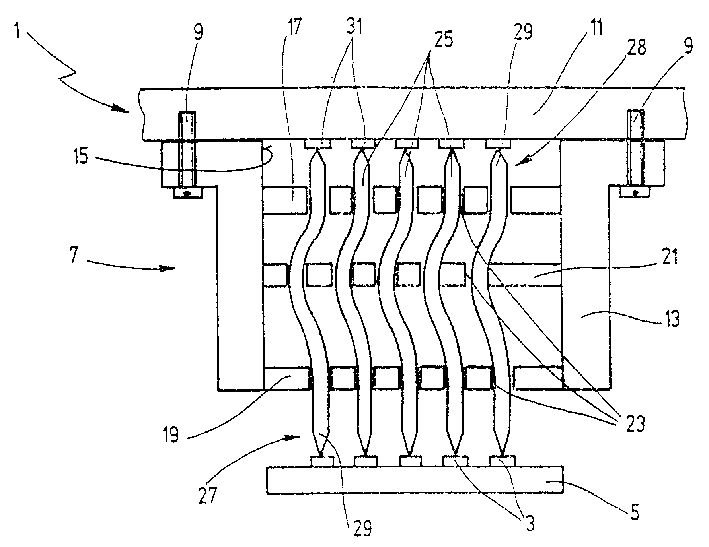
图1是本发明的检测头的第一实施例的原理示意图。Fig. 1 is a schematic diagram of the principle of the first embodiment of the detection head of the present invention.
图2是本发明的检测头的第二实施例的原理示意图。Fig. 2 is a schematic diagram of the principle of the second embodiment of the detection head of the present invention.
图3和图4分别是本发明的检测头的其它实施例的剖视示意图。Fig. 3 and Fig. 4 are schematic cross-sectional views of other embodiments of the detection head of the present invention, respectively.
下面描述的检测头用于检测检测点小并被相邻排列的电子结构元件。这种检测头普遍适用于例如在半导体技术范围内精密印刷电路板和半导体晶片的电试验。The inspection head described below is used for inspection of electronic structural components whose inspection spots are small and arranged adjacently. Such test heads are generally suitable for electrical testing of precision printed circuit boards and semiconductor wafers, for example within semiconductor technology.
图1示出用同时接触一电检测件5的多个相邻排列的检测点3的检测头1的第一实施例的原理图。检测头1包括一个接触装置7,它靠固定件9以可拆卸方式与检测装置的连接元件11相连,例如印刷电路板,它包括一个检测电源或类似物。在此实施例中,固定件9是由备有外螺纹的螺丝构成,在图1中仅画出了两个螺丝。螺丝在这里各拧穿过检测头1的座体13中的一个钻孔,拧紧于不很清楚画出的连接元件11中的螺纹钻孔中。加固件自然也可以由针连接元件、轴插孔、连接元件或者由夹子,弹簧或相类似物构成。重要的是,连接元件11与接触装置7的组合应以可拆卸方式连接,使固定件在两部份分开后不被损坏。FIG. 1 shows a schematic diagram of a first embodiment of a test head 1 for simultaneously contacting a plurality of adjacently arranged test points 3 of an
接触装置7包括一套筒型座体13,它有一通路孔15,在其中一第一导板17,一第二导板19和一第三导板21相互平行并相隔一个距离的被保护住。在导板17、19、21中该馈入通孔23,在其中针型接触体元件25也作为试验探头能被可轴向位移导引。在按图1检测头1的示图中只画出5个接触体元件25。这里所讨论类型的检测头1可包括直至几千个接触体元件25。接触体元件25由弹性的,最好是弹簧弹性材料制成,例如金属弹簧,在这里接触体元件25是弯折导线。导板17、19,21主要由非导电材料,例如人造材料、玻璃、陶瓷、硅或类似物制成。在另一图中未画出的实施例中的接触体元件的导引件包括代替或附加于导板的导引元件,其厚度大于导板厚度。The contact device 7 comprises a sleeve-
由图1看出,与各接触体元件25相配的第一导板17和第二导板19上的馈入通孔是相互齐平排列的。在第一和第二导板之间的中间空间中安置的第三导板21的相配馈入通孔23是偏离导板17、19上的馈入通孔的。由此在馈入通孔23中安置的接触体元件25成一曲线或一被弯曲的形状。通过调准接触体元件25垂直于其长度伸展方向,则在接触体元件25和导板17、19、21的相配的馈入通孔中的至少一个之间形成摩擦配合。接触体元件25最终通过摩擦被持住于接触装置7的座体13中。有效地阻止了接触体元件25从馈入通孔中跌落或滑出。It can be seen from FIG. 1 that the feeding through holes on the
接触体元件25在其与检测件5的检测点3相对的自由端27和在其与连接元件11相对的自由端28上各形成一接触尖29,在此处是通过针型接触体元件尖化制成。接触体元件25能用其与检测点3相背的自由端28挤压相应装配的接触位置31,在图1所示之实施例中它是装于检测装置的连接元件11上的,接触体元件25的自由端27能触压相配之检测件5上的检测点3。The
下面根据一检测过程进一步叙述检测头1的功能。在图1所画出的接触装置7的功能位置中接触体元件25既与检测件5的检测点3接触,也与连接元件11上的接触位置31相接触。通过接触装置7和检测件5的相对运动,接触体元件25在导板19和导板21的馈入通孔23中被轴向位移。通过针型接触体元件25在长度方向所受之压力由第三导板21的馈入通孔偏离设置而导致已变弯曲了的接触体元件25被偏斜。这时由接触体元件材料的弹性特性而产生的弹力对接触体元件25的触尖29有区别的压迫,检测件5的检测点3和连接元件11上的接触位置31,由此达到一较小的电接触电阻。现在检测点3能够在连续性和绝缘上相互来回的被监视或者检测件5在功能上被监视。在检测过程结束后,将接触装置7和检测件5分开。被变偏斜/变弯曲的接触体元件25基于其弹性特性自动返回其初始位置。The function of the detection head 1 is further described below according to a detection process. In the functional position of the contact device 7 depicted in FIG. 1 , the
很清楚、连接元件11上的接触位置31用于作为接触体元件25的支座。在图1中未画出的检测头实施例中预见到,接触体元件25在检测头1的准备就绪位置中被安置得与接触位置31保持一个距离。于是,在接触检测点3时接触体元件25被轴向位移直至它抵达接触位置31。至此接触体元件25才能进一步被弯曲并这样产生了使接触体元件25的触尖触压相应各检测点或者各接触位置31的接触力。It is clear that the
在图1中画出的检测头1的实施例通过一非常可靠的结构设计和对例如各种不同的检测件和/或者检测参量的高适应性被展示出来。The exemplary embodiment of the test head 1 shown in FIG. 1 is demonstrated by a very reliable design and a high adaptability, for example, to various test elements and/or test variables.
图2粗略地给出了检测头1的另外一种实施例。与图1中的部分相一致的部分用相同关系符号表示,使得这部分引证于图1的描述。下面只进一步讨论其差别。FIG. 2 schematically shows another embodiment of the test head 1 . Parts corresponding to those in FIG. 1 are denoted by the same relational symbols, so that this part is referred to in the description of FIG. 1 . Only the differences are discussed further below.
接触装置7藉助于在此实施例中由螺丝组成的固定件9以可拆卸的方式与一此处由一连接头33组成的检测装置的连接元件11相连接,在该元件11上装有接触位置31。螺丝在此处穿过在连接头中安置的通路钻孔并旋紧于在检测头1中的座体13中安置的螺纹钻孔上。接触位置31各与一导件(Line)35的自由端相连,该导件35通过未画出的插入型连接器或者直接与检测装置相连。导件35被固定于例如被粘连连接头33的孔37中。The contact device 7 is detachably connected to a
对图1和2画出之实施例来说共同之处是,接触装置7简单的能通过松开固定件9与检测头1的其余部分分开。从通路孔15的两个开口很容易接近接触体元件25,使得调换个别的接触体元件25变得容易了。由于接触体元件25能仅仅是摩擦贴切的被持住于导板17、19、21、的馈入通孔23中的至少一个,所以也完全可以从馈入通孔中取出它们并换上新的接触体元件。What is common to the exemplary embodiments shown in FIGS. 1 and 2 is that the contact device 7 can be separated from the rest of the test head 1 simply by loosening the
总结起来可肯定地说,基于图1和图2描述的检测头1提供了一简单的结构并因此可以合适的价格去制造,特别是,接触体元件能仅仅是摩擦贴切的在导板的馈入通孔中或者在导板之一的馈入通孔中摩擦贴切的被持住。用检测头可以检测精密结构的检测件,其检测点非常小并以很小的距离相互排列。其中靠尖化了的接触体元件或是接触体元件的触尖基于高的表面压力,不论在接触体元件和检测点之间还是在接触体元件和接触位置之间都可以达到好的电接触。To sum up, it can be said with certainty that the test head 1 described on the basis of FIGS. 1 and 2 provides a simple structure and can therefore be produced at a reasonable price. In particular, the contact element can only be frictionally fitted in the guide plate. The friction fit is held in the through hole or in the feed through hole of one of the guide plates. Precision-structured test parts can be tested with the test head, whose test points are very small and arranged at a small distance from each other. The sharpened contact element or the tip of the contact element is based on high surface pressure, and good electrical contact can be achieved no matter between the contact element and the detection point or between the contact element and the contact position. .
图3示出检测头的第三种实施例的原理草图。相同部分备以相同关系符号,可以使得这部分引证前面的图形的描述。这里只对差别作进一步讨论。检测头1包括一个导引体,如在按图1和图2的实施例中一样,是三个彼此相隔一定距离的导板17、19、21,它们被固定于检测头1的座体13的通路孔15中。在导板17、19、21中对接触体元件25备有馈入通孔23,它们在本实施例中被相互齐平的排列安装。即是说,每个与一接触体元件相配的在导板中的馈入通孔23的长度轴是一个跟一个的安置于一条设想直线G上,在图3中用虚线表示。在导板17和导板21间的中间空间41中安置了一止动件43,在本实施例中主要是由可挠曲的材料制成的止动薄膜45。在此止动薄膜45中安置了与导板17、19、21中馈入通孔23齐平排列的馈入通孔47,在其中一个接触体元件摩擦贴切的被持住。即是说,馈入通孔47的直径至少在截面上小于接触体元件的外直径。止动薄膜45能在导板17、21之间沿双箭头49方向自由移动。基于安置止动薄膜45于导板17、21之间和接触体元件摩擦贴切的持住于馈入通孔中,所以避免了接触体元件25从接触装置7中滑出或落掉。自然也可以使止动薄膜45不移动固定于座体13的通路孔15中,使得紧张起来的止动膜45在检测过程中仅仅区域性地被偏斜或者被弯曲。FIG. 3 shows a schematic sketch of a third exemplary embodiment of the test head. Identical parts are prepared with the same relational symbols, making it possible for this part to refer to the description of the previous figures. Only the differences are discussed further here. The detection head 1 comprises a guide body, as in the embodiment according to FIGS. via
在图3描述的检测件实施例的实施实验中可以预见到,与一接触体元件25相配的第一导板17和第二导板19的馈入通孔23被相互齐平的安装,使得在导板17、19间安置和第三导板21的相配的馈入通孔23与其它导板的馈入通孔23偏离。于是带进馈入通孔的接触体元件沿垂直于其长度方向偏斜,使得它们成为一个弓。因此,预先给了接触体元件一个优先方向,在此方向上接触体元件在加压下被偏调。换言之,通过导板的相互偏离或者置于其中的馈入通孔的相互错位可以调节接触体元件的最佳折向。在此检测头实施实验中特别有利的是,通过在装校状态下接触体元件的被弯曲形状可以将为折叠接触体元件所需之力完全消除。止动薄膜45中的馈入通孔47也能与导板17、19、21中至少一个的馈入通孔的偏离安置,这一点是完全清楚的。It can be foreseen in the implementation experiment of the detecting element embodiment described in Fig. 3 that the feed-through
在又一个优点众多的实施例中可以预见,止动件43,例如是主要由可挠曲材料制成的止动薄膜或弹胶物(Elastomer)层,被置于导板17、21中的至少一个上,例如在与中间空间45相对的导板的那个边上。因此检测头1的制造,特别是装校被简化了。In yet another advantageous embodiment, it is foreseeable that a stopper 43, such as a stopper film or layer of elastic (Elastomer) mainly made of a flexible material, is placed in at least one of the
图4示出检测头1的另一实施例判断,它包括具有座体13的接触装置7,用固定元件将连接元件11可拆卸的连结于接触装置7上。装于连接元件11上的接触位置31在此处是通过偏平带电缆51与检测装置相连。在此实施例中接触装置7只包括两个导板17、19,它们相互平行和相距一个距离在座体13的通路孔15中被固定。在导板17、19中设置的馈入通孔23中安置了接触体元件25,在其长度伸展方向以段的方式加上电绝缘层53。基于绝缘层53,接触体元件25表现为一直径较大的一段55和一与其衔接的直径较小的一段57。于是直径差通过在第一段55范围内的绝缘而形成。接触体元件25以其直径较小的第二段57被可移动的导入导板19的各相配的馈入通孔23和以其直径较大的第一段55被可移动的导入导板17的各相配之馈入通孔23中。Fig. 4 shows another embodiment of the detection head 1, which includes a contact device 7 with a
在导板19中的馈入通孔23安置直径小于第一段55范围内接触体元件。由此可以确定,接触体元件25由于重力的原因不能在检测件5的方向上从接触装置7中落出。在与检测件5相背的接触装置7的那一面接触体元件25也同样保证不会滑落出来,因为那里在座体13中的通路孔15通过可拆卸装于座体13上的连接元件11被遮盖住了。The feed-through
第一段55给出一直径d1和直径较小的第二段57给出一直径d2,它们对应于接触体元件25的外径。正如从图4中可以看出,第一段55的长度是这样选择的,在接触体元件25未加负荷状态下,例如在两个检测过程之间,在接触体元件25的触尖29和连接元件11上的接触位置31之间有一已知狭缝A在将检测头1放在检测件上或者相反,接触体元件25在轴的方向上被位移,直至触尖29达到接触位置31为止。通过在接触体元件25加上压力它就在导板17、19间的中间空间中沿垂直于长度伸展方向被调准,使得通过材料的弹性性质而产生的弹力,接触体元件的触尖就压迫检测点3和接触位置31。The first section 55 has a diameter d 1 and the second, smaller diameter section 57 has a diameter d 2 , which correspond to the outer diameter of the
在此实施例中,直径差d1-d2是通过第二段57的消绝缘而形成的。即是说,接触体元件25首先完全制备上绝缘层,之后在第二段57的范围内和在触尖处再去除掉。如下做法也是可能的,直径差,从接触体元件的第一段55到与其相连的第二段57的过渡可以如下进行,即,从一开始就只在第一段55的范围内覆盖一电绝缘层。只绝缘到接触体元件的一个被确定了的长度,使得可以简化接触体元件的制造,因为直径差能在一步加工中完成。In this embodiment, the diameter difference d 1 -d 2 is formed by de-insulating the second section 57 . That is to say that the
在基于图4描述的检测头的实施例的一个实施实验中,导板17、19中各与接触体元件相配的馈入通孔23是这样相互偏离安置的,使得在其中引入的接触体元件表现出一被弯曲的形状。由此就完全消除了折力并给出一最佳方向,接触体元件在加压力于其端部时,例如在一个检测过程中,沿此最佳方向被偏离。In an implementation experiment based on the embodiment of the test head described in FIG. 4 , the feed-through
所有按图1到图4描述的检测头1的实施例之共同点是,接触体元件25以简单和因此成本合适的方式靠止动件在接触装置7之中或近旁被持住,使得能避免接触体元件25由导板的馈入通孔中滑出。止动件是例如由两个具有相互偏离排列的馈入通孔的导板组成,在这些馈入通孔中,接触体元件摩擦贴切的和预先被弯曲不会丢失的被持住,基于这样的止动件结构,接触体元件能被特别紧密的相邻排列,使得具有检测点紧密网格排列的检测件也能完全被检测。除此之外更有利的是,连接元件11和接触装置7是可拆卸相连的,由此保证了从馈入通孔两边向在座体13的通路孔15中被持住的接触体元件25接近的易接近性,再者,各按接触体元件的实施实验从通路孔15两边调换单个接触体元件成为可能。What is common to all the embodiments of the test head 1 described in FIGS. It is prevented that the
通过连接元件和接触装置无损伤的和简单的分开性较快的调换这些部份之一成为可能。更进一步,用于检测检测件多个表现检测点不同网格布局的实施形式的检测头也能被使用了。这其中仅需接触元件用相应的另一种形式的接触元件来替换。A quick exchange of one of these parts is made possible by the damage-free and simple detachment of the connecting element and the contact device. Furthermore, for the inspection of the inspection piece multiple inspection heads representing different grid layouts of the inspection points can also be used. All that is required here is to replace the contact element with a correspondingly different type of contact element.
Claims (20)
Applications Claiming Priority (6)
| Application Number | Priority Date | Filing Date | Title |
|---|---|---|---|
| DE19748823.4 | 1997-11-05 | ||
| DE19748823A DE19748823B4 (en) | 1997-11-05 | 1997-11-05 | Service-friendly contacting device |
| DE19749456.0 | 1997-11-10 | ||
| DE19749456 | 1997-11-10 | ||
| DE19829934.6 | 1998-07-04 | ||
| DE19829934A DE19829934C2 (en) | 1997-11-05 | 1998-07-04 | Test head for microstructures with interface |
Publications (2)
| Publication Number | Publication Date |
|---|---|
| CN1227351A CN1227351A (en) | 1999-09-01 |
| CN1137384C true CN1137384C (en) | 2004-02-04 |
Family
ID=27217891
Family Applications (1)
| Application Number | Title | Priority Date | Filing Date |
|---|---|---|---|
| CNB981239684A Expired - Lifetime CN1137384C (en) | 1997-11-05 | 1998-11-04 | Test head for microstructures with interface |
Country Status (6)
| Country | Link |
|---|---|
| US (1) | US6150830A (en) |
| EP (1) | EP0915344B1 (en) |
| JP (1) | JP3252323B2 (en) |
| CN (1) | CN1137384C (en) |
| AT (1) | ATE260470T1 (en) |
| TW (1) | TW409439B (en) |
Families Citing this family (48)
| Publication number | Priority date | Publication date | Assignee | Title |
|---|---|---|---|---|
| US20020053734A1 (en) | 1993-11-16 | 2002-05-09 | Formfactor, Inc. | Probe card assembly and kit, and methods of making same |
| US6483328B1 (en) | 1995-11-09 | 2002-11-19 | Formfactor, Inc. | Probe card for probing wafers with raised contact elements |
| US6468098B1 (en) * | 1999-08-17 | 2002-10-22 | Formfactor, Inc. | Electrical contactor especially wafer level contactor using fluid pressure |
| US7396236B2 (en) | 2001-03-16 | 2008-07-08 | Formfactor, Inc. | Wafer level interposer |
| JP2002296295A (en) * | 2001-03-29 | 2002-10-09 | Isao Kimoto | Contact-holding structure for contact assembly |
| JP2002296297A (en) * | 2001-03-29 | 2002-10-09 | Isao Kimoto | Contact assembly |
| EP1438591A1 (en) * | 2001-10-10 | 2004-07-21 | Delaware Capital Formation, Inc. | Coaxial tilt pin fixture for testing high frequency circuit boards |
| US6447339B1 (en) * | 2001-12-12 | 2002-09-10 | Tektronix, Inc. | Adapter for a multi-channel signal probe |
| FR2838194B1 (en) * | 2002-04-04 | 2004-06-18 | Probest | MAINTENANCE APPARATUS FOR PIN CONNECTOR OF ELECTRONIC MICRO-CIRCUIT TEST SYSTEM |
| US6768331B2 (en) * | 2002-04-16 | 2004-07-27 | Teradyne, Inc. | Wafer-level contactor |
| CN100356183C (en) * | 2002-07-23 | 2007-12-19 | 井上商事株式会社 | Checking tool for printed circuit-board |
| US7122760B2 (en) * | 2002-11-25 | 2006-10-17 | Formfactor, Inc. | Using electric discharge machining to manufacture probes |
| US6945827B2 (en) * | 2002-12-23 | 2005-09-20 | Formfactor, Inc. | Microelectronic contact structure |
| KR100573089B1 (en) * | 2003-03-17 | 2006-04-24 | 주식회사 파이컴 | Probe and its manufacturing method |
| WO2005050706A2 (en) * | 2003-11-14 | 2005-06-02 | Wentworth Laboratories, Inc. | Die design with integrated assembly aid |
| US7046020B2 (en) * | 2004-02-17 | 2006-05-16 | Agilent Technologies, Inc. | Probes with perpendicularly disposed spring pins, and methods of making and using same |
| TWI286606B (en) * | 2004-03-16 | 2007-09-11 | Gunsei Kimoto | Electric signal connecting device, and probe assembly and prober device using it |
| US7230437B2 (en) * | 2004-06-15 | 2007-06-12 | Formfactor, Inc. | Mechanically reconfigurable vertical tester interface for IC probing |
| EP1870714A4 (en) * | 2005-03-31 | 2010-05-19 | Octec Inc | MICROSTRUCTURE SENSOR CARD AND MICROSTRUCTURE VERIFICATION DEVICE, METHOD, AND COMPUTER PROGRAM |
| US7271606B1 (en) * | 2005-08-04 | 2007-09-18 | National Semiconductor Corporation | Spring-based probe pin that allows kelvin testing |
| JP4823617B2 (en) | 2005-09-09 | 2011-11-24 | 日本発條株式会社 | Conductive contact and method for manufacturing conductive contact |
| JP3849948B1 (en) * | 2005-11-16 | 2006-11-22 | 日本電産リード株式会社 | Substrate inspection jig and inspection probe |
| TWI273247B (en) * | 2005-11-24 | 2007-02-11 | Mjc Probe Inc | Microhole guide plate with enhanced structure |
| US7323892B1 (en) * | 2006-06-07 | 2008-01-29 | Agilent Technologies, Inc. | Probe having a frame to align spring pins perpendicularly to a printed circuit board, and method of making same |
| TWM309110U (en) * | 2006-07-13 | 2007-04-01 | Lih Duo Int Co Ltd | Testing card for wafer quality |
| CN200968943Y (en) * | 2006-09-22 | 2007-10-31 | 鸿富锦精密工业(深圳)有限公司 | Part fixation test system |
| US20080100323A1 (en) * | 2006-10-25 | 2008-05-01 | Silicon Test Systems, Inc. | Low cost, high pin count, wafer sort automated test equipment (ate) device under test (dut) interface for testing electronic devices in high parallelism |
| DE102007057815A1 (en) * | 2006-12-19 | 2008-06-26 | Feinmetall Gmbh | Contacting device for a contact contacting of an electrical test specimen and corresponding method |
| JP2009025164A (en) * | 2007-07-19 | 2009-02-05 | Tokugen:Kk | Inspecting tool and method of manufacturing the same |
| JP5030060B2 (en) * | 2007-08-01 | 2012-09-19 | 軍生 木本 | Electrical signal connection device |
| US9069011B2 (en) * | 2009-09-11 | 2015-06-30 | Exelon Generation Company, Llc | Electrical terminal test point and methods of use |
| DE102012016449A1 (en) * | 2012-08-16 | 2014-03-13 | Feinmetall Gmbh | Test head for the electrical test of a test object |
| DE102013203536B4 (en) * | 2013-03-01 | 2016-03-31 | Multitest Elektronische Systeme Gmbh | Device for testing electronic components |
| JP2018503805A (en) * | 2014-12-04 | 2018-02-08 | テクノプローベ エス.ピー.エー. | Test head with vertical probe |
| CN107003335B (en) * | 2015-01-04 | 2020-05-22 | 金日 | contact test device |
| WO2016146499A1 (en) | 2015-03-13 | 2016-09-22 | Technoprobe S.P.A. | Testing head with vertical probes having an improved sliding movement within respective guide holes and correct holding of the probes within the testing head under different operative conditions |
| JP6728219B2 (en) * | 2015-03-31 | 2020-07-22 | テクノプローベ エス.ピー.エー. | Vertical contact probe for high frequency applications and test head with vertical contact probe |
| JP6855185B2 (en) | 2016-07-27 | 2021-04-07 | 株式会社日本マイクロニクス | Electrical connection device |
| JP6832661B2 (en) * | 2016-09-28 | 2021-02-24 | 株式会社日本マイクロニクス | Probe card and contact inspection device |
| CN106783656B (en) * | 2016-12-05 | 2019-11-29 | 武汉新芯集成电路制造有限公司 | A kind of probe structure for WAT detection machine |
| IT201700021397A1 (en) | 2017-02-24 | 2018-08-24 | Technoprobe Spa | Measuring head with improved frequency properties |
| JP2018179721A (en) * | 2017-04-12 | 2018-11-15 | 株式会社日本マイクロニクス | Electrical connection device |
| DE102017209510A1 (en) * | 2017-06-06 | 2018-12-06 | Feinmetall Gmbh | Contact Element System |
| TWI620938B (en) * | 2017-07-21 | 2018-04-11 | 中華精測科技股份有限公司 | Probe device |
| CN110068711B (en) * | 2018-01-24 | 2022-04-26 | 台湾中华精测科技股份有限公司 | Probe card device and rectangular probe |
| TWI766154B (en) | 2019-03-27 | 2022-06-01 | 旺矽科技股份有限公司 | Probe head and probe card |
| IT201900014208A1 (en) * | 2019-08-07 | 2021-02-07 | Technoprobe Spa | Measuring head of electronic devices and relative measuring card |
| EP4075149A3 (en) | 2021-04-12 | 2022-12-28 | Kes Systems & Service (1993) Pte Ltd. | Probe assembly for test and burn-in having a compliant contact element |
Family Cites Families (21)
| Publication number | Priority date | Publication date | Assignee | Title |
|---|---|---|---|---|
| JPS5491873U (en) * | 1977-12-13 | 1979-06-29 | ||
| US4423376A (en) * | 1981-03-20 | 1983-12-27 | International Business Machines Corporation | Contact probe assembly having rotatable contacting probe elements |
| DE3123627A1 (en) * | 1981-06-15 | 1982-12-30 | Siemens AG, 1000 Berlin und 8000 München | DEVICE FOR SIMULTANEOUSLY CONTACTING MULTIPLE CLOSE-UP CHECK POINTS, IN PARTICULAR OF GRID FIELDS |
| CH661129A5 (en) * | 1982-10-21 | 1987-06-30 | Feinmetall Gmbh | CONTACT DEVICE. |
| US4622514A (en) * | 1984-06-15 | 1986-11-11 | Ibm | Multiple mode buckling beam probe assembly |
| EP0283545B1 (en) * | 1987-03-27 | 1991-10-16 | Ibm Deutschland Gmbh | Contact-pins arrangement for the electrical contacting of a test device with circular contact surfaces of a test sample |
| JP2539453B2 (en) * | 1987-09-11 | 1996-10-02 | 株式会社日立製作所 | Semiconductor element inspection equipment |
| US4931726A (en) * | 1987-06-22 | 1990-06-05 | Hitachi, Ltd. | Apparatus for testing semiconductor device |
| JPH0833414B2 (en) * | 1987-11-26 | 1996-03-29 | 東京エレクトロン株式会社 | Probing card |
| US4901013A (en) * | 1988-08-19 | 1990-02-13 | American Telephone And Telegraph Company, At&T Bell Laboratories | Apparatus having a buckling beam probe assembly |
| WO1990006518A1 (en) * | 1988-11-28 | 1990-06-14 | Cimm, Inc. | Wireless test fixture |
| US5399982A (en) * | 1989-11-13 | 1995-03-21 | Mania Gmbh & Co. | Printed circuit board testing device with foil adapter |
| JP2516245Y2 (en) * | 1991-10-15 | 1996-11-06 | 株式会社ヨコオ | Conductive contact pin |
| US5415559A (en) * | 1992-05-18 | 1995-05-16 | Japan Aviation Electronics Industry, Ltd. | Electrical connector having a plurality of contact pin springs |
| JP2971706B2 (en) * | 1993-08-04 | 1999-11-08 | 株式会社ヨコオ | Probe card and coaxial probe needle terminal processing method |
| US5493230A (en) * | 1994-02-25 | 1996-02-20 | Everett Charles Technologies, Inc. | Retention of test probes in translator fixtures |
| US5451883A (en) * | 1994-04-07 | 1995-09-19 | Vlsi | Spring probe contactor with device stop for testing PGA devices and method therefor |
| JP3720887B2 (en) * | 1994-11-18 | 2005-11-30 | 富士通株式会社 | Contact device |
| JPH09113537A (en) * | 1995-10-17 | 1997-05-02 | Nippon Denshi Zairyo Kk | Vertical operation type probe card |
| JP2972595B2 (en) * | 1996-09-25 | 1999-11-08 | 日本電気ファクトリエンジニアリング株式会社 | Probe card |
| JP3038114U (en) * | 1996-11-22 | 1997-06-06 | 日本電子材料株式会社 | Probe with insulating coating and probe card using the same |
-
1998
- 1998-10-28 EP EP98120166A patent/EP0915344B1/en not_active Expired - Lifetime
- 1998-10-28 AT AT98120166T patent/ATE260470T1/en active
- 1998-11-02 TW TW087118201A patent/TW409439B/en not_active IP Right Cessation
- 1998-11-04 CN CNB981239684A patent/CN1137384C/en not_active Expired - Lifetime
- 1998-11-05 US US09/186,860 patent/US6150830A/en not_active Expired - Lifetime
- 1998-11-05 JP JP35065098A patent/JP3252323B2/en not_active Expired - Fee Related
Also Published As
| Publication number | Publication date |
|---|---|
| TW409439B (en) | 2000-10-21 |
| JP3252323B2 (en) | 2002-02-04 |
| EP0915344A3 (en) | 2001-01-31 |
| EP0915344B1 (en) | 2004-02-25 |
| EP0915344A2 (en) | 1999-05-12 |
| US6150830A (en) | 2000-11-21 |
| JPH11248747A (en) | 1999-09-17 |
| ATE260470T1 (en) | 2004-03-15 |
| CN1227351A (en) | 1999-09-01 |
Similar Documents
| Publication | Publication Date | Title |
|---|---|---|
| CN1137384C (en) | Test head for microstructures with interface | |
| JP3215946B2 (en) | Test head for microstructure with interface | |
| CN1180264C (en) | Probes for circuit board test setups | |
| US6515496B2 (en) | Microstructure testing head | |
| CN101345360B (en) | Socket adaptor apparatus | |
| EP3156805A1 (en) | Probe pin and electronic device using same | |
| US9733299B2 (en) | Inspection jig | |
| KR100989300B1 (en) | Board inspection jig and inspection probe | |
| CN100442057C (en) | Conductive contact probe | |
| CN1116709C (en) | Assembly device for semiconductor components | |
| EP0962776A3 (en) | Probe card suitable for inspection of multi-pin devices | |
| TWI680299B (en) | Linear probe fixture | |
| CN1582397A (en) | Roller contact with conductive brushes | |
| CN1668929A (en) | Assembly for electrically connecting a test component to a testing machine for testing electrical circuits on the test component | |
| US6255832B1 (en) | Flexible wafer level probe | |
| JP4863466B2 (en) | Manufacturing method of substrate inspection jig | |
| CN1146730C (en) | Easy-to-use contact device | |
| TW200541007A (en) | Test device for electrical testing of a unit under test | |
| CN1979194B (en) | Electrical testing device and corresponding method for testing electrical samples | |
| CN1204615C (en) | Electronic device measuring device and method | |
| JP2006234428A (en) | Contact probe and inspection device | |
| US6407568B1 (en) | Apparatus for probing ends of pins | |
| KR20200115103A (en) | Electrical Contactor and Probe Card | |
| WO2015076360A1 (en) | Socket attaching structure and spring member | |
| JP5353968B2 (en) | Substrate inspection jig |
Legal Events
| Date | Code | Title | Description |
|---|---|---|---|
| C10 | Entry into substantive examination | ||
| SE01 | Entry into force of request for substantive examination | ||
| C06 | Publication | ||
| PB01 | Publication | ||
| C14 | Grant of patent or utility model | ||
| GR01 | Patent grant | ||
| CX01 | Expiry of patent term | ||
| CX01 | Expiry of patent term |
Granted publication date: 20040204 |