CN113772675A - Purification method of semiconductor grade silicon powder - Google Patents
Purification method of semiconductor grade silicon powder Download PDFInfo
- Publication number
- CN113772675A CN113772675A CN202111337818.9A CN202111337818A CN113772675A CN 113772675 A CN113772675 A CN 113772675A CN 202111337818 A CN202111337818 A CN 202111337818A CN 113772675 A CN113772675 A CN 113772675A
- Authority
- CN
- China
- Prior art keywords
- silicon powder
- mbar
- furnace
- purity
- purified
- Prior art date
- Legal status (The legal status is an assumption and is not a legal conclusion. Google has not performed a legal analysis and makes no representation as to the accuracy of the status listed.)
- Withdrawn
Links
- XUIMIQQOPSSXEZ-UHFFFAOYSA-N Silicon Chemical compound [Si] XUIMIQQOPSSXEZ-UHFFFAOYSA-N 0.000 title claims abstract description 51
- 239000011863 silicon-based powder Substances 0.000 title claims abstract description 49
- 239000004065 semiconductor Substances 0.000 title claims abstract description 18
- 238000000034 method Methods 0.000 title claims abstract description 17
- 238000000746 purification Methods 0.000 title abstract description 11
- 238000010438 heat treatment Methods 0.000 claims abstract description 28
- 239000007789 gas Substances 0.000 claims abstract description 24
- VEXZGXHMUGYJMC-UHFFFAOYSA-N Hydrochloric acid Chemical compound Cl VEXZGXHMUGYJMC-UHFFFAOYSA-N 0.000 claims abstract description 19
- IXCSERBJSXMMFS-UHFFFAOYSA-N hydrogen chloride Substances Cl.Cl IXCSERBJSXMMFS-UHFFFAOYSA-N 0.000 claims abstract description 19
- 229910000041 hydrogen chloride Inorganic materials 0.000 claims abstract description 19
- XKRFYHLGVUSROY-UHFFFAOYSA-N Argon Chemical compound [Ar] XKRFYHLGVUSROY-UHFFFAOYSA-N 0.000 claims abstract description 12
- 230000006698 induction Effects 0.000 claims abstract description 12
- 229910052786 argon Inorganic materials 0.000 claims abstract description 6
- OKTJSMMVPCPJKN-UHFFFAOYSA-N Carbon Chemical compound [C] OKTJSMMVPCPJKN-UHFFFAOYSA-N 0.000 claims description 9
- 229910002804 graphite Inorganic materials 0.000 claims description 8
- 239000010439 graphite Substances 0.000 claims description 8
- 238000005086 pumping Methods 0.000 claims description 8
- 238000005273 aeration Methods 0.000 claims description 5
- HBMJWWWQQXIZIP-UHFFFAOYSA-N silicon carbide Chemical compound [Si+]#[C-] HBMJWWWQQXIZIP-UHFFFAOYSA-N 0.000 abstract description 15
- 239000000463 material Substances 0.000 abstract description 4
- 238000012545 processing Methods 0.000 abstract description 3
- 239000012535 impurity Substances 0.000 description 15
- 229910052751 metal Inorganic materials 0.000 description 14
- 239000002184 metal Substances 0.000 description 14
- IJGRMHOSHXDMSA-UHFFFAOYSA-N Atomic nitrogen Chemical compound N#N IJGRMHOSHXDMSA-UHFFFAOYSA-N 0.000 description 12
- 239000013078 crystal Substances 0.000 description 8
- 229910052757 nitrogen Inorganic materials 0.000 description 6
- 229910010271 silicon carbide Inorganic materials 0.000 description 6
- 239000002994 raw material Substances 0.000 description 5
- 239000000126 substance Substances 0.000 description 5
- 150000001875 compounds Chemical class 0.000 description 4
- 239000000843 powder Substances 0.000 description 4
- 239000000758 substrate Substances 0.000 description 4
- 230000009286 beneficial effect Effects 0.000 description 3
- 238000009835 boiling Methods 0.000 description 3
- -1 chlorine radicals Chemical class 0.000 description 3
- 238000001816 cooling Methods 0.000 description 3
- 230000000694 effects Effects 0.000 description 3
- 238000002474 experimental method Methods 0.000 description 3
- 239000001257 hydrogen Substances 0.000 description 3
- 229910052739 hydrogen Inorganic materials 0.000 description 3
- 238000002347 injection Methods 0.000 description 3
- 239000007924 injection Substances 0.000 description 3
- 238000004806 packaging method and process Methods 0.000 description 3
- 239000000460 chlorine Substances 0.000 description 2
- 229910052801 chlorine Inorganic materials 0.000 description 2
- 230000007547 defect Effects 0.000 description 2
- 238000007599 discharging Methods 0.000 description 2
- 238000000605 extraction Methods 0.000 description 2
- 150000002431 hydrogen Chemical class 0.000 description 2
- 230000005855 radiation Effects 0.000 description 2
- 238000007789 sealing Methods 0.000 description 2
- 229910052710 silicon Inorganic materials 0.000 description 2
- 239000010703 silicon Substances 0.000 description 2
- 239000000243 solution Substances 0.000 description 2
- JBRZTFJDHDCESZ-UHFFFAOYSA-N AsGa Chemical compound [As]#[Ga] JBRZTFJDHDCESZ-UHFFFAOYSA-N 0.000 description 1
- 229910001218 Gallium arsenide Inorganic materials 0.000 description 1
- 230000015556 catabolic process Effects 0.000 description 1
- 238000004140 cleaning Methods 0.000 description 1
- 239000008358 core component Substances 0.000 description 1
- 238000011161 development Methods 0.000 description 1
- 230000005684 electric field Effects 0.000 description 1
- 238000005265 energy consumption Methods 0.000 description 1
- 238000005516 engineering process Methods 0.000 description 1
- 238000004880 explosion Methods 0.000 description 1
- 229910052736 halogen Inorganic materials 0.000 description 1
- 150000002367 halogens Chemical class 0.000 description 1
- 238000004519 manufacturing process Methods 0.000 description 1
- 229910001510 metal chloride Inorganic materials 0.000 description 1
- 150000002736 metal compounds Chemical class 0.000 description 1
- 238000004377 microelectronic Methods 0.000 description 1
- 238000013508 migration Methods 0.000 description 1
- 230000005012 migration Effects 0.000 description 1
- 231100000956 nontoxicity Toxicity 0.000 description 1
- 230000005693 optoelectronics Effects 0.000 description 1
- 239000002210 silicon-based material Substances 0.000 description 1
- 238000001179 sorption measurement Methods 0.000 description 1
- 230000002194 synthesizing effect Effects 0.000 description 1
Images
Classifications
-
- C—CHEMISTRY; METALLURGY
- C01—INORGANIC CHEMISTRY
- C01B—NON-METALLIC ELEMENTS; COMPOUNDS THEREOF; METALLOIDS OR COMPOUNDS THEREOF NOT COVERED BY SUBCLASS C01C
- C01B33/00—Silicon; Compounds thereof
- C01B33/02—Silicon
- C01B33/037—Purification
Landscapes
- Chemical & Material Sciences (AREA)
- Organic Chemistry (AREA)
- Inorganic Chemistry (AREA)
- Silicon Compounds (AREA)
Abstract
The invention discloses a purification method of semiconductor grade silicon powder, belonging to the technical field of semiconductor material processing; firstly, putting silicon powder to be purified in an induction heating furnace, and heating to 1000-1300 ℃ in a vacuum state; the vacuum degree is 4.5-5.5 multiplied by 10‑ 6mbar; then high-purity H is injected into the furnace chamber2To 700 and 900 mbar; then vacuumizing to the original vacuum degree; introducing hydrogen chloride and argon into the cavity at a flow ratio of 7-9:1.5-2.5, introducing the gas to a pressure of 700-; the invention effectively improves the purity of the silicon powder, and the purified silicon powder meets the purity requirement of producing high-purity silicon carbide powder; and simultaneously, the danger of the whole purification process is reduced.
Description
Technical Field
The invention belongs to the technical field of semiconductor material processing, and particularly relates to a purification method of semiconductor grade silicon powder.
Background
With the rapid development of semiconductors and the progress of microelectronic technology, the requirements of high voltage resistance, high temperature resistance, radiation resistance, high frequency and high reliability are provided for core components, and the traditional silicon and gallium arsenide devices are close to the working limit and cannot meet the requirements. The third generation semiconductor silicon carbide has the properties of wide forbidden band, high thermal conductivity, high electron saturation migration rate, high breakdown electric field and the like, and the characteristics determine that the third generation semiconductor silicon carbide has great potential in overcoming the contradiction between power and frequency of power electronic devices and improving the high temperature resistance and the radiation resistance of semiconductor devices, and is considered as an ideal semiconductor material for manufacturing optoelectronic devices, high-frequency high-power devices and high-temperature electronic devices. Wherein the high-purity semi-insulating silicon carbide single crystal substrate is a key substrate material of the GaN power device. The high-purity silicon carbide powder is a raw material for growing the high-purity semi-insulating silicon carbide single crystal substrate, and the purity of the powder directly influences the growth quality, resistivity and other electrical properties of the silicon carbide single crystal.
At present, graphite powder and silicon powder are generally used as raw materials to synthesize high-purity silicon carbide powder, so the purity of the raw material silicon for synthesizing the powder needs to be controlled in order to control the purity of the powder. However, at present, silicon powder is generally prepared by mechanically crushing and cleaning a large silicon material, although metal impurities contained in the silicon powder are greatly reduced, the purity of the silicon powder still cannot meet the requirement of preparing high-purity silicon carbide powder, and meanwhile, because the silicon powder has small granularity, large surface energy and easy nitrogen adsorption, the metal impurities and the nitrogen content in the silicon carbide powder prepared by directly using the silicon powder are high, and various defects in crystals can be induced to generate and influence the electrical properties of the crystals when single crystal growth is carried out.
Disclosure of Invention
The invention overcomes the defects of the prior art and provides a purification method of semiconductor grade silicon powder to improve the purity of the silicon powder, so that the purified silicon powder meets the purity requirement of producing high-purity silicon carbide powder.
In order to achieve the purpose, the invention is realized by the following technical scheme:
a purification method of semiconductor grade silicon powder comprises the following steps:
a) putting the silicon powder to be purified in an induction heating furnace, and heating to 1000-1300 ℃ in a vacuum state; vacuum degree of 4.5X 10⁻⁶-5.5×10⁻⁶mbar; then high-purity H is injected into the furnace chamber2To 700 and 900 mbar; maintaining for 10-20min, and vacuumizing to 4.5 × 10⁻⁶-5.5×10⁻⁶mbar。
b) The temperature in the furnace is continuously increased to 1600-2000 ℃, hydrogen chloride and argon are introduced into the cavity according to the flow ratio of 7-9:1.5-2.5, the gas is introduced until the pressure is 700-900mbar, the gas is kept for 4-6 h, and then the pressure in the furnace is reduced to less than 10 mbar.
Preferably, in the step a, the furnace body is slowly heated to 1200 ℃ at a heating rate of 10 ℃/min in a vacuum state in the induction heating furnace.
Preferably, in step a, high purity H is injected2The aeration speed of (2) is 1.5-2.5L/min.
Preferably, in step b, the pressure in the furnace is reduced to < 10 mbar with a gas evacuation rate of 10 mbar/min.
Preferably, the operation of step b is performed after repeating the operation of step a 5-6 times, and the operation of step b is also repeated 5-6 times.
Preferably, the silicon powder to be purified is placed in a graphite crucible and then placed in an induction heating furnace.
Preferably, after the step b is finished, under the protection of Ar, the induction heating furnace is slowly cooled to room temperature, the furnace is opened, and the purified silicon powder is taken out and packaged.
Compared with the prior art, the invention has the following beneficial effects:
the invention utilizes the small molecular size of hydrogen, can be fully diffused in the gaps of the raw materials, and is beneficial to discharging nitrogen in the gaps of the silicon powder. At the same time H2High thermal conductivity, H2Can be sufficiently diffused in the gaps of the silicon powder, and therefore, passes through H2The heat conduction can fully heat the silicon powder, fully desorb the gas adsorbed on the surface, and can follow H in the air extraction process2Viscous airflow escapes from the crucible, so that the nitrogen removal effect is further improved. And (3) reacting the hydrogen chloride with the metal simple substance and the compound impurities thereof in the silicon powder at a high temperature to remove the metal impurities. Meanwhile, the dried hydrogen chloride gas has low price, no toxicity, no flammability and no explosion, has high safety and can be continuously applied for a long time.
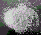
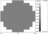
According to the invention, silicon powder is further purified, and the purified silicon powder meets the purity requirement of producing high-purity silicon carbide powder; the purified silicon powder growing powder is white and transparent; the wafer obtained after crystal processing has uniform resistivity which is larger than 1E10 omega cm, and meets the requirement of a high-purity semi-insulating silicon carbide single crystal substrate; the temperature required in the whole purification process is lower, so that the energy consumption is further reduced, and the risk of the whole purification process is also reduced.
Drawings
FIG. 1 is a silicon carbide powder prepared using the silicon powder purified in example 1;
FIG. 2 is a resistivity profile of a wafer made from the silicon carbide powder of FIG. 1.
Detailed Description
In order to make the technical problems, technical solutions and advantageous effects to be solved by the present invention more clearly apparent, the present invention is further described in detail with reference to the embodiments and the accompanying drawings. It should be understood that the specific embodiments described herein are merely illustrative of the invention and are not intended to limit the invention. The technical solution of the present invention is described in detail below with reference to the embodiments and the drawings, but the scope of protection is not limited thereto.
Example 1
1. Putting the silicon powder to be purified in a graphite crucible, putting the graphite crucible in an induction heating hearth, sealing, and vacuumizing the furnace chamber to 5 multiplied by 10 when the heating is not started-6mbar, then slowly heating the furnace body to 1200 deg.C at a heating rate of 10 deg.C/min under vacuum, maintaining the temperature, and injecting high purity H into the furnace chamber at an aeration rate of 2L/min2To 800mbar, held for 15 minutes and then evacuated to 5X 10⁻⁶mbar, which is a pump cycle, followed by a second injection of high purity H2To 800mbar, for 15 minutes, and subsequently to 5X 10⁻⁶mbar, which was repeated 5 times in cycles such that the vacuum in the apparatus was maintained at 5X 10⁻⁶mbar. The purpose of the step is to mainly utilize the small molecular size of hydrogen, which can be fully diffused in the gap of the raw material and is beneficial to discharging nitrogen in the gap of the silicon powder. At the same time H2High thermal conductivity, and from the above, H2Can be sufficiently diffused in the gaps of the silicon powder, and therefore, passes through H2The heat conduction can fully heat the silicon powder, fully desorb the gas adsorbed on the surface, and can follow H in the air extraction process2Viscous airflow escapes from the crucible, so that the nitrogen removal effect is further improved.
2. And continuously heating the temperature in the furnace to 1600 ℃, introducing hydrogen chloride and argon into the cavity according to the flow ratio of 8:2, introducing the gas until the pressure is 800mbar, stopping introducing the gas, maintaining the gas for 5 hours, fully reacting the hydrogen chloride gas in the cavity with metal impurities, then reducing the pressure of the furnace body from 800mbar to a near vacuum state (< 10 mbar) at a pumping speed of 10 mbar/min, so as to perform a hydrogen chloride introducing pumping and filling cycle, and repeating the cycle for 5 times to finish the process. The aim of the step is to remove metal impurities by reacting hydrogen chloride with metal simple substances and compound impurities thereof in silicon powder at high temperature.
3. And finally, slowly cooling to room temperature under the protection of Ar, opening the furnace, taking out the purified silicon powder, packaging and finishing the experiment.
In this embodiment, a "halogen gas purification" process is added after the high-temperature purification process, that is, hydrogen chloride gas is introduced at a high-temperature stage, and the dried hydrogen chloride gas is dissociated into chlorine radicals and hydrogen radicals at a temperature above 1600 ℃.

Wherein the chlorine free radical can react with the high boiling point metal simple substance and the metal compound to generate the low boiling point metal chloride impurity. Thus, high boiling point impurities can be removed by repeatedly pumping air, and the purity of the silicon powder is further improved.
Example 2
1. Putting the silicon powder to be purified in a graphite crucible, putting the graphite crucible in an induction heating hearth, sealing, and vacuumizing the furnace chamber to 4.5 multiplied by 10 when the heating is not started-6mbar, then slowly heating the furnace body to 1000 deg.C at a heating rate of 10 deg.C/min under vacuum, maintaining the temperature, and injecting high purity H into the furnace chamber at an aeration rate of 2.5L/min2To 700mbar, for 20 minutes, and then to 4.5X 10⁻⁶mbar, which is a pump cycle, followed by a second injection of high purity H2To 700mbar for 15 minutes, and subsequently to 4.5X 10⁻⁶mbar, which was repeated 6 times in cycles such that the vacuum in the apparatus was maintained at 4.5X 10⁻⁶mbar。
2. And continuously heating the temperature in the furnace to 2000 ℃, introducing hydrogen chloride and argon into the cavity according to the flow ratio of 9:2.5, introducing the gas until the pressure is 700mbar, stopping introducing the gas, maintaining the gas for 5 hours, fully reacting the hydrogen chloride gas in the cavity with metal impurities, then reducing the pressure of the furnace body from 700mbar to a near vacuum state at a pumping speed of 10 mbar/min, and performing hydrogen chloride introduction pumping and filling circulation repeatedly for 5 times to finish the process. The aim of the step is to remove metal impurities by reacting hydrogen chloride with metal simple substances and compound impurities thereof in silicon powder at high temperature.
3. And finally, slowly cooling to room temperature under the protection of Ar, opening the furnace, taking out the purified silicon powder, packaging and finishing the experiment.
Example 3
1. Putting the silicon powder to be purified into a graphite crucible, putting the graphite crucible into an induction heating hearth, and sealingThe furnace chamber is vacuumized to 5.5 x 10 when heating is not started-6mbar, then slowly heating the furnace body to 1300 deg.C under vacuum at a heating rate of 10 deg.C/min, maintaining the temperature, and injecting high purity H into the furnace chamber at an aeration rate of 1.5L/min2To 900mbar, for 20 minutes and then to 5.5X 10⁻⁶mbar, which is a pump cycle, followed by a second injection of high purity H2To 900mbar for 15 minutes, and subsequently to 5.5X 10⁻⁶mbar, which was repeated 6 times in cycles such that the vacuum in the apparatus was maintained at 5.5X 10⁻⁶mbar。
2. And continuously heating the temperature in the furnace to 1800 ℃, introducing hydrogen chloride and argon into the cavity according to the flow ratio of 7:1.5, introducing the gas until the pressure is 900mbar, stopping introducing the gas, maintaining the gas for 5 hours, fully reacting the hydrogen chloride gas in the cavity with metal impurities, then reducing the pressure of the furnace body from 900mbar to a near vacuum state at a pumping speed of 10 mbar/min, and performing hydrogen chloride introduction pumping and filling circulation repeatedly for 5 times to finish the process. The aim of the step is to remove metal impurities by reacting hydrogen chloride with metal simple substances and compound impurities thereof in silicon powder at high temperature.
3. And finally, slowly cooling to room temperature under the protection of Ar, opening the furnace, taking out the purified silicon powder, packaging and finishing the experiment.
While the invention has been described in further detail with reference to specific preferred embodiments thereof, it will be understood by those skilled in the art that various changes in form and details may be made therein without departing from the spirit and scope of the invention as defined by the appended claims.
Claims (7)
1. The method for purifying the semiconductor grade silicon powder is characterized by comprising the following steps of:
a) putting the silicon powder to be purified in an induction heating furnace, and heating to 1000-1300 ℃ in a vacuum state; vacuum degree of 4.5X 10⁻⁶-5.5×10⁻⁶mbar; then in the furnace chamberInjecting high purity H2To 700 and 900 mbar; maintaining for 10-20min, and vacuumizing to 4.5 × 10⁻⁶-5.5×10⁻⁶mbar;
b) The temperature in the furnace is continuously increased to 1600-2000 ℃, hydrogen chloride and argon are introduced into the cavity according to the flow ratio of 7-9:1.5-2.5, the gas is introduced until the pressure is 700-900mbar, the gas is kept for 4-6 h, and then the pressure in the furnace is reduced to less than 10 mbar.
2. The method for purifying semiconductor grade silicon powder according to claim 1, wherein in the step a, the furnace body is slowly heated to 1200 ℃ in the induction heating furnace at a heating rate of 10 ℃/min in a vacuum state.
3. The method for purifying semiconductor grade silicon powder according to claim 1, wherein in the step a, high purity H is injected2The aeration speed of (2) is 1.5-2.5L/min.
4. The method according to claim 1, wherein in step b, the pressure in the furnace body is reduced to < 10 mbar at a pumping rate of 10 mbar/min.
5. The method for purifying semiconductor grade silicon powder according to claim 1, wherein the operation of step b is performed after the operation of step a is repeated 5-6 times, and the operation of step b is also repeated 5-6 times.
6. The method according to claim 1, wherein the silicon powder to be purified is placed in a graphite crucible and then placed in an induction furnace.
7. The method for purifying semiconductor grade silicon powder according to claim 1, wherein after step b is finished, under the protection of Ar, the induction heating furnace is slowly cooled to room temperature, opened, and the purified silicon powder is taken out and packaged.
Priority Applications (1)
| Application Number | Priority Date | Filing Date | Title |
|---|---|---|---|
| CN202111337818.9A CN113772675A (en) | 2021-11-12 | 2021-11-12 | Purification method of semiconductor grade silicon powder |
Applications Claiming Priority (1)
| Application Number | Priority Date | Filing Date | Title |
|---|---|---|---|
| CN202111337818.9A CN113772675A (en) | 2021-11-12 | 2021-11-12 | Purification method of semiconductor grade silicon powder |
Publications (1)
| Publication Number | Publication Date |
|---|---|
| CN113772675A true CN113772675A (en) | 2021-12-10 |
Family
ID=78873886
Family Applications (1)
| Application Number | Title | Priority Date | Filing Date |
|---|---|---|---|
| CN202111337818.9A Withdrawn CN113772675A (en) | 2021-11-12 | 2021-11-12 | Purification method of semiconductor grade silicon powder |
Country Status (1)
| Country | Link |
|---|---|
| CN (1) | CN113772675A (en) |
Citations (9)
| Publication number | Priority date | Publication date | Assignee | Title |
|---|---|---|---|---|
| BE669917A (en) * | 1964-09-21 | 1966-01-17 | ||
| CN101007633A (en) * | 2006-12-15 | 2007-08-01 | 佟新廷 | Silicon preparation method of PV industry |
| CN101462716A (en) * | 2008-05-05 | 2009-06-24 | 陈怀军 | Preparation technique for purifying graphite by high temperature method |
| CN101475174A (en) * | 2009-01-23 | 2009-07-08 | 晶海洋半导体材料(东海)有限公司 | Method for purifying industrial silicon for preparing solar grade silicon |
| CN101481111A (en) * | 2009-01-23 | 2009-07-15 | 晶海洋半导体材料(东海)有限公司 | Method for preparing high-purity silicon by high temperature gas-solid reaction |
| CN101805921A (en) * | 2010-04-22 | 2010-08-18 | 孙国志 | Preparation method of polycrystalline silicon |
| CN102009978A (en) * | 2011-01-06 | 2011-04-13 | 四川永祥多晶硅有限公司 | Polysilicon production method |
| CN107857241A (en) * | 2017-09-01 | 2018-03-30 | 河南中汇新材科技有限公司 | High-purity silicon nitride powder production technology |
| CN112919473A (en) * | 2021-04-22 | 2021-06-08 | 山西烁科晶体有限公司 | Method for synthesizing low-nitrogen high-purity silicon carbide powder |
-
2021
- 2021-11-12 CN CN202111337818.9A patent/CN113772675A/en not_active Withdrawn
Patent Citations (9)
| Publication number | Priority date | Publication date | Assignee | Title |
|---|---|---|---|---|
| BE669917A (en) * | 1964-09-21 | 1966-01-17 | ||
| CN101007633A (en) * | 2006-12-15 | 2007-08-01 | 佟新廷 | Silicon preparation method of PV industry |
| CN101462716A (en) * | 2008-05-05 | 2009-06-24 | 陈怀军 | Preparation technique for purifying graphite by high temperature method |
| CN101475174A (en) * | 2009-01-23 | 2009-07-08 | 晶海洋半导体材料(东海)有限公司 | Method for purifying industrial silicon for preparing solar grade silicon |
| CN101481111A (en) * | 2009-01-23 | 2009-07-15 | 晶海洋半导体材料(东海)有限公司 | Method for preparing high-purity silicon by high temperature gas-solid reaction |
| CN101805921A (en) * | 2010-04-22 | 2010-08-18 | 孙国志 | Preparation method of polycrystalline silicon |
| CN102009978A (en) * | 2011-01-06 | 2011-04-13 | 四川永祥多晶硅有限公司 | Polysilicon production method |
| CN107857241A (en) * | 2017-09-01 | 2018-03-30 | 河南中汇新材科技有限公司 | High-purity silicon nitride powder production technology |
| CN112919473A (en) * | 2021-04-22 | 2021-06-08 | 山西烁科晶体有限公司 | Method for synthesizing low-nitrogen high-purity silicon carbide powder |
Non-Patent Citations (3)
| Title |
|---|
| KULKARNI, MB ET AL.: "Methane enrichment of biogas produced from floral waste: A potential energy source for rural India", 《ENERGY SOURCES PART A-RECOVERY UTILIZATION AND ENVIRONMENTAL EFFECTS 》 * |
| 杨振伟: "微硅粉湿法提纯制备球形纳米二氧化硅", 《中国优秀硕士学位论文全文数据库 工程科技Ⅰ辑》 * |
| 王家鑫等: "硅粉在冷等离子体中的刻蚀纯化", 《第六届中国功能材料及其应用学术会议论文集(2)》 * |
Similar Documents
| Publication | Publication Date | Title |
|---|---|---|
| CN104775149B (en) | A kind of method and device for growing high-purity semi-insulating silicon carbide monocrystalline | |
| CN112647130B (en) | A kind of method for growing gallium oxide thin film by low pressure chemical vapor deposition | |
| CN109722712B (en) | Method for uniformly doping SiC single crystal metal impurities | |
| CN111484019A (en) | Preparation method of high-purity silicon carbide powder for single crystal growth | |
| CN105417541A (en) | Method for preparing high-purity silicon carbide powder | |
| CN106711022A (en) | Preparation method for growing silicon carbide epitaxial film with clear doping interface | |
| EP1375423B1 (en) | Use of a low nitrogen concentration carbonaceous material as a jig. | |
| CN104947182A (en) | Method for rapidly growing large-size high-purity semi-insulating silicon carbide single crystal | |
| CN114182357A (en) | Method for regrowing silicon carbide single crystal by using broken crystal grains of silicon carbide crystal | |
| CN109183143B (en) | Method for improving AlN single crystal purity by using reducing gas | |
| CN104878445A (en) | Preparation method of low-dosage concentration silicon carbide epitaxial material | |
| CN107699955A (en) | It is a kind of using microwave heat remove single-crystal silicon carbide defect in and surface organic impurities method | |
| JPH09246196A (en) | Method for producing silicon single crystal and silicon single crystal thin film | |
| CN113735110B (en) | Purification method of semiconductor-grade graphite powder | |
| CN113594267A (en) | Method for forming oxide layer | |
| CN1265444C (en) | Method for preparing half insulated substrate by using non-adulterated indium phosphide through high temperature annealing | |
| CN114182341B (en) | A high-purity crystal growth system and method | |
| CN113818085B (en) | System and method for uniform growth of nitride single crystal by flux method | |
| CN117238756A (en) | SiC ion implantation post-annealing process | |
| TWI912218B (en) | Purification method of high purity graphite block for semiconductor | |
| CN114203527A (en) | Method and device for thermal oxidation of silicon carbide wafer | |
| CN113716566A (en) | Preparation method of high-purity silicon carbide source powder | |
| CN117735544B (en) | Deep purification method of semiconductor grade graphite powder | |
| CN104233219A (en) | Method for preparing P-type heavily-doped silicon carbide thin film epitaxial layer by controlling doping source flow | |
| CN120273026A (en) | Production process of boron arsenide thin film crystal |
Legal Events
| Date | Code | Title | Description |
|---|---|---|---|
| PB01 | Publication | ||
| PB01 | Publication | ||
| SE01 | Entry into force of request for substantive examination | ||
| SE01 | Entry into force of request for substantive examination | ||
| WW01 | Invention patent application withdrawn after publication |
Application publication date: 20211210 |
|
| WW01 | Invention patent application withdrawn after publication |