Large-scale efficient direct-current transformer
Technical Field
The invention relates to the field of transformers, in particular to a large-scale efficient direct-current transformer.
Background
In the occasions of flexible direct current power transmission and distribution, rail transit, ships and warships and the like, the direct current transformer is key equipment for realizing voltage matching, electrical isolation and voltage regulation between the medium-voltage direct current bus and the low-voltage direct current bus. The input-series-output parallel-type combined converter has low voltage resistance and current resistance requirements on a switching device, and has the characteristics of modularization and easy expansibility, so that the input-series-output parallel-type combined converter becomes an ideal direct-current transformer form.
For the input-series output-parallel combined converter, the input voltage equalizing and the output current equalizing among all the sub-modules are ensured to ensure that the whole converter can normally operate. For this purpose, a number of advanced control methods are proposed: same duty cycle control, three-loop control, two-loop control, interconnection-less control, etc. The same duty ratio control is the simplest, but the input voltage-sharing and output current-sharing effects among the submodules are greatly influenced by the consistency of the parameters of the submodules. Therefore, in the document [1] "research on an input-series-output parallel system of a multi-converter module with a natural voltage-sharing characteristic", a two-stage structure of a boost converter cascade LLC-DCX is adopted as a submodule, and a control method with the same duty ratio is adopted to realize the stable operation of the whole direct-current transformer. The scheme improves the input voltage-sharing and output current-sharing degrees among the submodules, but reduces the conversion efficiency of the system. Document [2] "voltage decoupling control of a switched capacitor type ISOP converter" also adopts a two-stage structure, replaces LLC-DCX in document [1] with a phase-shifted full-bridge converter, and adopts voltage decoupling control to realize stable operation of a direct current transformer. The control system needs to adopt the input direct-current link capacitor voltage of each submodule, the cost is increased, and the pre-stage converter of the submodule is only used for fault removal.
The existing three-loop control and two-loop control strategies are complex, the input direct-current voltage of each submodule needs to be sampled, and the cost is increased. The interconnection-less control strategy has a softer out-of-output characteristic. The voltage-sharing and current-sharing effect in the same duty ratio control scheme adopting the single-stage structure is greatly influenced by the manufacturing process of the sub-module, and the system efficiency is not high by adopting the two-stage structure (boost + SRC) controlled by the same duty ratio.
Disclosure of Invention
The invention provides a large-scale efficient direct current transformer, which comprises a main circuit and a controller, wherein the controller is connected with the main circuit; the main circuit comprises at least two submodules, the input sides of the submodules are connected in series, and the output sides of the submodules are connected in parallel; the sub-module comprises a booster circuit and an isolated circuit, and the booster circuit is connected with the isolated circuit in a cascade way; the controller is respectively connected with the booster circuit and the isolation circuit of each submodule and is used for controlling a preceding stage booster circuit in each submodule so as to realize the control of the power flow direction or the output voltage or the input voltage;
the controller adopts a digital closed-loop control strategy, the output of the compensator is a modulation signal Vc, and when the large-scale high-efficiency direct-current transformer is in an optimal efficiency mode, the duty ratio of a boost circuit in each sub-module can be determined by judging the output of the modulation signal Vc and the carrier offset and amplitude set by each sub-module; when the large-scale high-efficiency direct current transformer is in a maximum power mode, the duty ratio of the boost circuit in each submodule can be obtained by dividing a modulation signal Vc by the number N of submodules and then sending the result to the carrier wave of each submodule.
As a further improvement of the present invention, the digital closed-loop control strategy comprises:
output voltage closed-loop control strategy: and generating a modulation signal Vc through output voltage closed loop, and generating and controlling the duty ratio of a Boost booster circuit in each submodule after the modulation signal Vc is subjected to carrier modulation, thereby realizing the regulation of the output voltage Vo.
As a further improvement of the present invention, the digital closed-loop control strategy further comprises:
input voltage closed-loop control strategy: and generating a modulation signal Vc through input voltage closed loop, and generating and controlling the duty ratio of a Boost booster circuit in each submodule after the modulation signal Vc is subjected to carrier modulation, thereby realizing the regulation of the input voltage Vin.
As a further improvement of the present invention, the digital closed-loop control strategy further comprises:
output voltage double closed loop control strategy: generating a reference signal i of a current inner loop by an output voltage outer looprefAnd generating a modulation signal Vc through the current inner ring, and generating and controlling the duty ratio of a Boost booster circuit in each submodule after the modulation signal Vc is subjected to carrier modulation, thereby realizing the regulation of the output voltage Vo.
As a further improvement of the present invention, the digital closed-loop control strategy further comprises:
input or output current closed-loop control strategy: and generating a modulation signal Vc through a current closed loop, and generating and controlling the duty ratio of a Boost booster circuit in each submodule after the modulation signal Vc is subjected to carrier modulation, thereby realizing the regulation of input or output current.
As a further improvement of the present invention, the controller includes a computing module and a carrier control module, the computing module is configured to provide a modulation signal to the voltage boost circuit in each of the sub-modules, the carrier control module is configured to provide a carrier to the voltage boost circuit in the sub-module, and the modulation signal and the carrier together form a driving signal of the voltage boost circuit; the controller comprises a fixed duty ratio and fixed frequency PWM generating module, and the fixed duty ratio and fixed frequency PWM generating module is used for providing a driving signal for the isolated circuit; the calculation module is a closed-loop voltage, current or power loop calculation module; the large-scale high-efficiency direct current transformer further comprises a hysteresis function block, and the hysteresis function block is used for preventing the converter from shaking between a maximum power mode and an optimal efficiency mode.
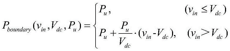
As a further improvement of the invention, the carrier wave will depend on the input power pinSum mode boundary power pboundaryWhen the input power p is greater than the maximum power carrier and the optimum efficiency carrierinIf the boundary power is less than-2 delta, switching from the maximum power mode to the optimal efficiency mode; when the input power pinWhen > mode boundary power-delta, switch from the optimum efficiency mode to the maximum power mode.
When switching from a maximum power mode to an optimum efficiency mode, a stacked carrier is selected as a carrier for each of the sub-modules; when switching from the optimal efficiency mode to the maximum power mode, a large carrier is selected as a carrier for each of the sub-modules;
the amplitude of the large carrier is the sum of the amplitudes of the laminated carriers of the booster circuits in the submodules; and if the maximum amplitude limit a of the duty ratio of the booster circuit in the submodule is set, the carrier offset of the ith submodule in the laminated carrier is (i-1) aH.
As a further development of the invention, the mode boundary power pboundaryIs about the input voltage vinA rated input power P that can be processed by a single sub-moduleuAnd the expected DC-link capacitance voltage V of a single said sub-moduledcAs shown in the following equation:
the isolation circuit has the characteristic of fixed voltage transformation ratio, so that the direct current link voltage Vdc and the output voltage Vo have the relation of fixed transformation ratio, and when the output voltage is stabilized at a desired voltage, the direct current link voltage Vdc is also stabilized at a fixed voltage value;
when the large-scale efficient direct current transformer works in an optimal efficiency mode, the lower tube duty ratio of the booster circuit in part of the submodules is 0.
As a further improvement of the invention, the isolated circuit is a series resonance circuit working under a fixed duty ratio or a phase-shifted full bridge under a fixed phase-shifting angle and fixed frequency or a double-active bridge circuit under a fixed phase-shifting angle and fixed frequency; the isolated circuit can adopt a structure of sharing one transformer magnetic core; the isolated circuit can further adopt a structure of sharing a secondary side rectifier on the basis of adopting a structure of sharing a transformer magnetic core; in the system starting stage of the large-scale high-efficiency direct current transformer, a maximum power mode is selected as a default starting mode, and after the system enters a steady state, the maximum power mode is used as a default starting mode according to input or output power and mode boundary power pboundaryDetermines in which mode the system operates; the input inductances in the boost circuits of the submodules can be combined into one inductance.
As a further improvement of the invention, the large-scale high-efficiency direct current transformer also comprisesWhen the system needs to be switched from the optimal efficiency mode to the expanded power mode, the carrier waves of the area where the modulation signal Vc is located and the carrier waves above the area are fused into a large carrier wave, the carrier waves of modules lower than the modulation signal Vc are kept unchanged, and meanwhile, the system is located in a work partition under different input voltage and input power conditions according to the input power PinAnd merge boundary power line Pfusion_boundary(x,Pu) The relationship of (a) determines whether the number of fused carriers needs to be increased to meet the power requirement;
the fusion boundary power line is a function of the number of carriers of the fusion sub-module and the rated power processed by the single sub-module, and is specifically shown by the following formula:
PFusion_boundary(x,Pu)=x·Pu(1<x≤N),
wherein N is the total number of the submodules;
when the input power Pin> (fuse boundary Power line P)fusion_boundary(x,Pu)-δ1) If so, increasing the number of the fusion carriers to at least (x + 1); when the input power Pin< (fuse boundary power line Pfusion_boundary(x,Pu)-2δ1) And then, the number of the fusion carriers can still meet the power requirement when the number is less than x.
The invention has the beneficial effects that: 1. the large-scale efficient direct-current transformer is simple in control structure, high in efficiency and easy to remove faults; 2. the large-scale efficient direct current transformer not only reduces the cost, but also improves the working efficiency.
Drawings
FIG. 1(a) is a main circuit diagram of the present invention;
FIG. 1(b) is a schematic block diagram of the controller of the present invention;
FIG. 2(a) is a schematic diagram of a stacked carrier of the present invention;
FIG. 2(b) is a schematic diagram of a large carrier according to the present invention;
FIG. 3 is a schematic diagram of a digital closed loop control strategy of the present invention, FIG. 3(a) is a schematic diagram of an output voltage closed loop control; FIG. 3(b) a schematic diagram of input voltage closed loop control; FIG. 3(c) output voltage dual closed loop control schematic; FIG. 3(d) input or output current closed loop control.
FIG. 4 is a schematic diagram of the system operating region for different input voltages and input powers of the present invention;
FIG. 5 is a series resonant circuit diagram of the present invention;
FIG. 6 is a circuit diagram of a dual active bridge of the present invention;
FIG. 7 is a phase-shifted full-bridge circuit diagram of the present invention;
FIG. 8 is a main circuit diagram of the common input inductor of the present invention;
FIG. 9 is a schematic diagram of the system operating region for different input voltages and input powers of the present invention;
fig. 10 is a schematic diagram of the fusion of carriers of two sub-modules of the present invention.
Detailed Description
As shown in fig. 1, the invention discloses a large-scale high-efficiency direct current transformer, wherein a main circuit in the invention is shown in fig. 1(a), the main circuit at least comprises two sub-modules, the input sides of the sub-modules are connected in series, the output sides of the sub-modules are connected in parallel, and each sub-module is formed by cascading a booster circuit and an isolation circuit.
Fig. 1(b) is a schematic block diagram of a control structure. The isolated circuit is a series resonance circuit working under a fixed duty ratio or a phase-shifted full bridge under a fixed phase-shifting angle and a fixed frequency or a double-active circuit under a fixed phase-shifting angle and a fixed frequency.
The invention realizes the control of the power flow direction or the output voltage or the input voltage by controlling the preceding stage booster circuit in each submodule through the controller.
The carrier in the present invention will depend on the input power pinSum mode boundary power pboundaryThe size relationship of (c) is switched between the maximum power carrier and the optimum efficiency carrier. By introducing a hysteresis block, the converter can be prevented from dithering between the maximum power mode and the optimum efficiency mode. When the input power < (boundary power-2 δ), then switching from the maximum power mode to the optimum efficiency mode, the stacked carriers as in fig. 2(a) are selected as the carriers for the respective sub-modules; when the input power is > (mode boundary power-delta), then from the optimal efficiency modeSwitching to the maximum power mode, a large carrier such as that of fig. 2(b) is selected as the carrier for each sub-module.
And the amplitude of the large carrier is the sum of the amplitudes of the laminated carriers of the boosting circuits of the submodules. And the amplitude of the carrier wave of each sub-module booster circuit in the laminated carrier wave is H. The carrier offset of the ith sub-module is (i-1) × H. And if the maximum amplitude limit a of the duty ratio of the booster circuit in the submodules is set, the carrier offset of the ith submodule in the laminated carrier is (i-1) a H.
The control strategy of the present invention is schematically illustrated in fig. 3. Fig. 3(a) is a schematic diagram of an output voltage closed-loop control strategy. And generating a modulation signal Vc through output voltage closed loop, and generating and controlling the duty ratio of a Boost booster circuit in each submodule after the modulation signal Vc is subjected to carrier modulation, thereby realizing the regulation of the output voltage Vo.
Fig. 3(b) is a schematic diagram of an input voltage closed-loop control strategy. The modulation signal Vc is generated through input voltage closed loop, and the modulation signal Vc is generated after carrier modulation to control the duty ratio of a Boost circuit in each submodule, so that the regulation of the input voltage Vin is realized.
Fig. 3(c) is a schematic diagram of an output voltage outer loop input or output current inner loop control strategy. Generating a reference signal i of a current inner loop by an output voltage outer looprefAnd a modulation signal Vc is generated through the current inner ring, and the modulation signal Vc is generated after carrier modulation to control the duty ratio of a Boost circuit in each submodule, so that the regulation of the output voltage Vo is realized.
FIG. 3(d) is a schematic diagram of an input or output current closed-loop control strategy. The modulation signal Vc is generated through current closed loop, and the modulation signal Vc is generated after carrier modulation to control the duty ratio of a Boost circuit in each submodule, so that the regulation of input or output current is realized.
When digital closed-loop control is adopted, the output of the compensator is a modulation signal Vc. When the system is in the optimal efficiency mode, the duty ratio of the boost circuit in each sub-module can be determined by judging Vc and the carrier offset and amplitude set by each sub-module. When the system is in a maximum power mode, the duty ratio of the boost circuit in each submodule can be obtained by dividing the modulation signal Vc by the number N of submodules and then sending the result to the carrier of each submodule (removing direct current bias), and the duty ratios of the modules are the same, so that the duty ratio can be conveniently and quickly calculated.
Mode boundary power pboundaryIs about the input voltage vinRated input power P that can be handled by individual submodulesuAnd expected dc-link capacitor voltage V for a single submoduledcAs shown in the following equation:
since the isolated circuit in the sub-module operates at a fixed frequency or a fixed moving angle with a fixed duty ratio, the isolated circuit has a characteristic of a fixed voltage transformation ratio, and therefore the direct-current link voltage Vdc and the output voltage Vo have a fixed transformation ratio relation. When the output voltage is stabilized at a desired voltage, the dc link voltage Vdc is also stabilized at a fixed voltage value.
When the input power of the direct current transformer is smaller than the mode boundary power, the whole direct current transformer works in the optimal efficiency mode, the lower tube duty ratio of the booster circuit in part of the sub-modules is 0, and therefore switching loss and reverse recovery loss in the main circuit are reduced.
The isolated circuit in the submodule may select a series resonant circuit as shown in fig. 5, which operates at a fixed duty cycle and a fixed frequency.
The isolated circuit in the sub-module may be selected as a dual active bridge circuit as shown in fig. 6, which operates at a fixed frequency with a fixed shift to the corner.
The isolated circuits in the submodules may be selected as phase-shifted full-bridge circuits as shown in fig. 7, which operate at a fixed frequency with a fixed shift to the angle.
The input inductors in each sub-module boost circuit may also be combined into one inductor, as shown in fig. 8.
The isolated circuits in each submodule can also adopt a structure of sharing one transformer magnetic core, so that the power density of the system can be improved.
The isolated circuits in the submodules can further share the structure of the secondary rectifier on the basis of the structure of sharing one transformer magnetic core, so that the power density is further improved.
In the system starting phase, the maximum power mode is selected as the default starting mode. When the system enters a steady state, the system starts to determine the mode in which the system operates according to the relation between the input or output power and the mode boundary power.
In addition, more detailed region division can be performed in the original maximum power region, but this will complicate system control, but will further improve system efficiency. Fig. 9 shows another working partition where the system is located under different input voltage and input power conditions. Wherein, the mode I is an extended power mode, and the mode II is still an optimal efficiency mode.
When the system needs to be switched from the optimal efficiency mode to the extended power mode, all modules do not share one large carrier wave for modulation any more, but the carrier wave in the area where the modulation signal Vc is located and the carrier waves above the area are fused into the large carrier wave, and the carrier waves of all modules lower than the modulation signal Vc are kept unchanged. At the same time, according to the input power PinAnd merge boundary power line Pfusion_boundary(x,Pu) The relationship determines whether the number of fused carriers needs to be increased to meet the power requirement. Fig. 10 shows a schematic diagram of the carrier fusion of two sub-modules, and the remaining carriers are unchanged.
The fused boundary power line is a function of the number of carriers of the fused sub-modules and the rated power processed by the single sub-module, and is shown by the following formula:
PFusion_boundary(x,Pu)=x·Pu (1<x≤N),
wherein N is the total number of sub-modules.
In the extended power mode, the system can be prevented from jittering between adjacent fusion states by introducing a hysteresis function block. When the input power Pin> (fuse boundary Power line P)fusion_boundary(x,Pu)-δ1) Then the carriers are fusedThe number is increased to at least (x + 1); when the input power Pin< (fuse boundary power line Pfusion_boundary(x,Pu)-2δ1) And then, the number of the fusion carriers can still meet the power requirement when the number is less than x.
The invention has the beneficial effects that: 1. the large-scale efficient direct-current transformer is simple in control structure, high in efficiency and easy to remove faults; 2. the large-scale efficient direct current transformer not only reduces the cost, but also improves the working efficiency.
The foregoing is a more detailed description of the invention in connection with specific preferred embodiments and it is not intended that the invention be limited to these specific details. For those skilled in the art to which the invention pertains, several simple deductions or substitutions can be made without departing from the spirit of the invention, and all shall be considered as belonging to the protection scope of the invention.