Disclosure of Invention
The invention provides a method and a device for controlling IPO thickness in SGT Mosfet and a computer readable storage medium, and mainly aims to solve the problems that high manpower and material resources are required to be consumed and the manufacturing cost is high when the phenomena of insufficient voltage resistance and electric leakage of a source electrode and a grid electrode are improved.
In order to achieve the above object, the present invention provides a method for controlling IPO thickness in SGT Mosfet, comprising:
obtaining a silicon groove substrate, and depositing pre-constructed non-doped silicon oxide and source polycrystalline silicon in a groove of the silicon groove substrate to obtain an initial deposition groove;
removing part of the undoped silicon oxide in the initial deposition groove according to a preset depth removal standard to obtain an original to-be-oxidized deposition groove;
implanting nitrogen atoms with preset concentration and energy on the surface of the source electrode polycrystalline silicon in the original groove to be oxidized and deposited by utilizing pre-constructed nitrogen implantation equipment to obtain a target polycrystalline silicon layer to be oxidized;
oxidizing the target polycrystalline silicon layer to be oxidized and the inner wall of the original groove to be oxidized and deposited to obtain an IPO (intrinsic polycrystalline silicon) oxide layer with the target thickness and a grid oxide layer with the target thickness respectively;
and depositing pre-constructed grid polysilicon on the surfaces of the target thickness IPO oxide layer and the target thickness grid oxide layer to finish the regulation and control of the IPO thickness.
Optionally, the obtaining the silicon trench substrate includes:
obtaining an original substrate, partitioning according to a preset SGT Mosfet structure, and determining an etching area on the surface of the original substrate;
and etching the original substrate on the etching area of the original substrate by utilizing a pre-constructed silicon groove etching process to obtain the silicon groove substrate.
Optionally, depositing the pre-formed undoped silicon oxide and the source polysilicon in the trench of the silicon trench substrate to obtain an initial deposition trench, including:
liquefying the undoped silicon oxide to obtain liquefied undoped silicon oxide;
adjusting the ambient temperature of the liquefied undoped silicon oxide to obtain gasified undoped silicon oxide;
uniformly depositing the gasified non-doped silicon oxide in the groove of the silicon groove substrate to obtain a silicon deposition groove covering a silicon deposition layer;
depositing the source electrode polycrystalline silicon in the silicon deposition groove to obtain a source electrode deposition groove;
and polishing the inner surface of the source electrode deposition groove and the source electrode polycrystalline silicon to obtain the initial deposition groove.
Optionally, the removing, according to a predetermined depth removal standard, a part of the undoped silicon oxide in the initial deposition trench to obtain an original deposition trench to be oxidized includes:
measuring and calculating the depth of source polycrystalline silicon in the initial deposition groove;
determining a removal depth value of the silicon deposition layer according to a preset depth removal standard and the depth of the source electrode polycrystalline silicon;
dividing the silicon deposition layer in the initial deposition groove according to the removal depth value to obtain a part of the silicon deposition layer to be removed;
and removing the part of the silicon deposition layer to be removed to obtain the original to-be-oxidized deposition groove.
Optionally, the implanting nitrogen atoms with a predetermined concentration and energy into the surface of the source polysilicon in the original to-be-oxidized deposition trench by using the pre-constructed nitrogen implantation apparatus to obtain the target to-be-oxidized polysilicon layer includes:
acquiring a target IPO thickness value, and preparing nitrogen atoms with target concentration and energy according to the target IPO thickness value by using the nitrogen implantation equipment;
and implanting nitrogen atoms with the target concentration and energy into the upper surface of the source electrode polycrystalline silicon by using the nitrogen implantation equipment to obtain the target polycrystalline silicon layer to be oxidized.
Optionally, before implanting nitrogen atoms with a predetermined concentration and energy on the surface of the source polysilicon in the original trench to be oxidized and deposited by using the pre-configured nitrogen implantation apparatus, the method further includes:
setting a nitrogen atom gradient set with gradually increased concentration and energy, and sequentially extracting nitrogen atom gradient values with different concentrations and energies in the nitrogen atom gradient set;
preparing nitrogen atoms with corresponding concentration and energy according to the nitrogen atom gradient value by using pre-constructed original nitrogen implantation equipment to obtain gradient nitrogen atoms to be detected;
implanting the gradient nitrogen atoms to be tested into the surface of the pre-constructed polycrystalline silicon and the surface of the silicon deposition body by using the original nitrogen implantation equipment to respectively obtain a testing polycrystalline silicon layer to be oxidized and a testing silicon deposition layer to be oxidized;
oxidizing the tested to-be-oxidized polycrystalline silicon layer and the tested to-be-oxidized silicon deposition layer to respectively obtain a tested polycrystalline silicon oxidation layer and a tested silicon deposition oxidation layer;
measuring the thickness values of the tested polysilicon oxide layer and the tested silicon deposition oxide layer to obtain a tested polysilicon oxidation thickness value and a tested silicon deposition oxidation thickness value;
constructing a nitrogen atom gradient-IPO thickness regulation table according to the nitrogen atom gradient set, each nitrogen atom gradient value and the corresponding test polysilicon oxidation thickness value;
constructing a nitrogen atom gradient-sedimentary deposit oxidation thickness regulation table according to the nitrogen atom gradient concentration, each nitrogen atom gradient value and the corresponding test silicon deposition oxidation thickness value;
and recording the nitrogen atom gradient-IPO thickness regulation table and the nitrogen atom gradient-deposition layer oxidation thickness regulation table into the original nitrogen implantation equipment to obtain the nitrogen implantation equipment.
Optionally, depositing pre-constructed gate polysilicon on the surfaces of the target thickness IPO oxide layer and the target thickness gate oxide layer to complete the IPO thickness regulation, including:
determining the depth of the grid polycrystalline silicon according to the oxidation thickness of the IPO oxide layer with the target thickness and the depth of the groove of the silicon groove substrate to obtain the depth value of the grid polycrystalline silicon;
and depositing the grid polysilicon above the IPO oxide layer with the target thickness according to the depth value of the grid polysilicon to obtain the SGT Mosfet with the target IPO thickness.
In order to solve the above problem, the present invention further provides a device for controlling IPO thickness in SGT Mosfet, the device comprising:
the initial deposition groove obtaining module is used for obtaining a silicon groove substrate, and depositing pre-constructed non-doped silicon oxide and source polycrystalline silicon in a groove of the silicon groove substrate to obtain an initial deposition groove;
the original to-be-oxidized deposition groove obtaining module is used for removing part of non-doped silicon oxide in the initial deposition groove according to a preset depth removal standard to obtain an original to-be-oxidized deposition groove;
the oxide layer thickness regulating module is used for implanting nitrogen atoms with preset concentration and energy on the surface of the source electrode polycrystalline silicon in the original groove to be oxidized and deposited by utilizing pre-constructed nitrogen implantation equipment to obtain a target polycrystalline silicon layer to be oxidized; oxidizing the target polycrystalline silicon layer to be oxidized and the inner wall of the original groove to be oxidized and deposited to obtain an IPO (intrinsic polycrystalline silicon) oxide layer with the target thickness and a grid oxide layer with the target thickness respectively;
and the grid polycrystalline silicon deposition module is used for depositing pre-constructed grid polycrystalline silicon on the surfaces of the target thickness IPO oxide layer and the target thickness grid oxide layer to finish the regulation and control of the IPO thickness.
In order to solve the above problem, the present invention also provides an electronic device, including:
at least one processor;
and a memory communicatively coupled to the at least one processor;
wherein the memory stores instructions executable by the at least one processor to enable the at least one processor to perform the controllable method of IPO thickness in SGT mosfets of any of claims 1 to 7.
In order to solve the above problem, the present invention further provides a computer-readable storage medium, where at least one instruction is stored, and the at least one instruction is executed by a processor in an electronic device to implement the above-mentioned method for controlling IPO thickness in SGT mosfets.
Compared with the background art: in the embodiment of the invention, the undoped silicon oxide and the source polysilicon are deposited in a pre-constructed silicon trench substrate to obtain an initial deposition trench, the undoped silicon oxide in the initial deposition trench is partially removed to obtain an original to-be-oxidized deposition trench, nitrogen atoms with preset concentration and energy are implanted into the surface of the source polysilicon by using the nitrogen implantation equipment in the process of oxidizing the original to-be-oxidized deposition trench to obtain a target to-be-oxidized polysilicon layer, and the target to-be-oxidized polysilicon layer and the inner wall of the original to-be-oxidized deposition trench are oxidized to obtain the target thickness IPO oxide layer and the target thickness gate oxide layer, and finally, depositing in a cavity defined by the IPO oxide layer with the target thickness and the grid oxide layer with the target thickness by utilizing the grid polysilicon to obtain the SGT Mosfet with the controllable IPO thickness. Therefore, the method, the device, the electronic equipment and the computer-readable storage medium for controlling the IPO thickness in the SGT Mosfet, provided by the invention, can solve the problems that higher manpower and material resources are required to be consumed and the manufacturing cost is higher when the phenomena of insufficient voltage resistance and electric leakage of a source electrode and a grid electrode are improved.
Detailed Description
It should be understood that the specific embodiments described herein are merely illustrative of the invention and are not intended to limit the invention.
The embodiment of the application provides a method for controlling the thickness of IPO in SGT Mosfet. The implementation subject of the method for controlling IPO thickness in SGT Mosfet includes, but is not limited to, at least one of electronic devices such as a server and a terminal that can be configured to perform the method provided by the embodiments of the present application. In other words, the method for controlling IPO thickness in SGT mosfets may be performed by software or hardware installed in a terminal device or a server device, and the software may be a block chain platform. The server includes but is not limited to: a single server, a server cluster, a cloud server or a cloud server cluster, and the like.
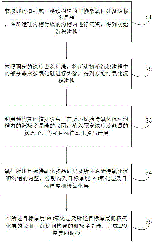
Fig. 1 is a schematic flow chart of a method for controlling an IPO thickness in an SGT Mosfet according to an embodiment of the present invention. In this embodiment, the method for controlling the IPO thickness in the SGT Mosfet includes:
and S1, obtaining a silicon trench substrate, and depositing the pre-constructed non-doped silicon oxide and the source polycrystalline silicon in the trench of the silicon trench substrate to obtain an initial deposition trench.
Illustratively, the silicon trench substrate refers to a carrier carrying semiconductor field effect transistor related components. The non-doped silicon oxide Glass (NSG) refers to a layer of non-doped silicon material deposited on the surface of the silicon trench substrate. The Source polysilicon (Source Poly) is polysilicon deposited at the bottom of the trench after the undoped silicon oxide is deposited on the silicon trench substrate, and is used for connecting a Source.
In detail, referring to fig. 2, the obtaining a silicon trench substrate includes:
s11, obtaining an original substrate, partitioning according to a preset SGT Mosfet structure, and determining an etching area on the surface of the original substrate;
and S12, etching the original substrate on the etching area of the original substrate by utilizing a pre-constructed silicon groove etching process to obtain the silicon groove substrate.
It can be understood that before etching the original substrate, the position to be etched and the etching shape are already defined, and when etching is needed, the etching is only needed to be carried out according to the preset position.
In the embodiment of the present invention, the depositing the pre-formed undoped silicon oxide and the source polysilicon in the trench of the silicon trench substrate to obtain an initial deposition trench includes:
liquefying the undoped silicon oxide to obtain liquefied undoped silicon oxide;
adjusting the ambient temperature of the liquefied undoped silicon oxide to obtain gasified undoped silicon oxide;
uniformly depositing the gasified non-doped silicon oxide in the groove of the silicon groove substrate to obtain a silicon deposition groove covering a silicon deposition layer;
depositing the source electrode polycrystalline silicon in the silicon deposition groove to obtain a source electrode deposition groove;
and polishing the inner surface of the source electrode deposition groove and the source electrode polycrystalline silicon to obtain the initial deposition groove.
It should be understood that the silicon deposition layer refers to a deposition layer formed by depositing the undoped silicon oxide in the trench of the silicon trench substrate. The non-doped silicon oxide can be prepared by introducing the gasified non-doped silicon oxide and other gases required by reaction into the groove of the silicon groove substrate by using a chemical vapor deposition method, and uniformly generating the silicon deposition layer on the inner surface of the groove, so that the silicon deposition layer is deposited on the surface of the inner wall of the groove of the silicon groove substrate, and the deposited thickness is consistent.
In the embodiment of the invention, the Source polysilicon (Source Poly) often forms a tip in shape, which is easy to cause tip discharge, so that the Source polysilicon is leaked, and the phenomenon can be effectively relieved by polishing the Source polysilicon.
And S2, removing part of the undoped silicon oxide in the initial deposition groove according to a preset depth removal standard to obtain the original to-be-oxidized deposition groove.
Understandably, after the undoped silicon oxide and the source polysilicon are deposited in the trench of the silicon trench substrate, the undoped silicon oxide needs to be partially removed, and only a part of the undoped silicon oxide layer in contact with the source polysilicon, namely, NSG, remains. The depth removal standard refers to a removal standard for removing a part of the undoped silicon oxide layer. The to-be-oxidized deposition groove is an unoxidized deposition groove obtained after part of the undoped silicon oxide layer is removed according to the depth removal standard.
In detail, referring to fig. 3, the removing a portion of the undoped silicon oxide in the initial deposition trench according to the predetermined depth removal criterion to obtain an original to-be-oxidized deposition trench includes:
s21, measuring and calculating the depth of the source polycrystalline silicon in the initial deposition groove;
s22, determining the removal depth value of the silicon deposition layer according to the depth of the source electrode polycrystalline silicon according to a preset depth removal standard;
s23, dividing the silicon deposition layer in the initial deposition groove according to the removal depth value to obtain a silicon deposition layer removal part;
and S24, removing the part of the silicon deposition layer to be removed to obtain the original to-be-oxidized deposition groove.
It will be appreciated that the depth to which the silicon deposition layer should be removed can be determined by the depth of deposition of the source polysilicon in the initial deposition trench. By keeping the relative position distance between the source electrode polycrystalline silicon and the silicon deposition layer within a certain range, the prepared SGT Mosfet can be ensured to meet the use standard.
Explicably, the depth of the source polysilicon refers to a distance value from a lowest point of the source polysilicon within the initial deposition trench to a highest point of an outer surface. The depth removal standard is a standard for defining a removal depth value of the silicon deposition layer according to the depth of the source polycrystalline silicon. The undoped silicon oxide layer may typically be made slightly higher than the source polysilicon.
And S3, implanting nitrogen atoms with preset concentration and energy into the surface of the source electrode polycrystalline silicon in the original groove to be oxidized and deposited by utilizing the pre-constructed nitrogen implantation equipment to obtain the target polycrystalline silicon layer to be oxidized.
Illustratively, the nitrogen implantation apparatus is capable of receiving a user input oxide layer thickness value and an oxidation portion, and implanting nitrogen atoms with corresponding concentration and energy at the oxidation portion in the original trench to be oxidized according to the oxide layer thickness.
In an embodiment of the present invention, the implanting nitrogen atoms with a predetermined concentration and energy into the surface of the source polysilicon in the original trench to be oxidized and deposited by using the pre-constructed nitrogen implantation apparatus to obtain the target polysilicon layer to be oxidized includes:
acquiring a target IPO thickness value, and preparing nitrogen atoms with target concentration and energy according to the target IPO thickness value by using the nitrogen implantation equipment;
and implanting nitrogen atoms with the target concentration and energy into the upper surface of the source electrode polycrystalline silicon by using the nitrogen implantation equipment to obtain the target polycrystalline silicon layer to be oxidized.
Understandably, similar to the B, P implant, the energy of the nitrogen implant is about 20-200kev, and the concentration of implanted nitrogen is about 10^13-10^16 atoms
. The thickness of the oxide layer in the subsequent oxidation process is controlled by the concentration and energy value of the implanted nitrogen atoms. Typically, the target IPO thickness value may range from 2 to 5 times the thickness of the oxide layer that has not been implanted with nitrogen atoms.
It should be understood that, during the process of implanting nitrogen atoms into the upper surface of the source polysilicon, nitrogen atoms may be implanted into the upper surface of the silicon deposition body of the original to-be-oxidized deposition trench by using the nitrogen implantation apparatus according to the nitrogen atom gradient-deposition layer oxidation thickness regulation table in the nitrogen implantation apparatus, and generally, the value of the oxide layer thickness range of the upper surface of the silicon deposition body may be about 1.5 times the thickness of the oxide layer that has not been implanted by nitrogen atoms.
In detail, the nitrogen atom implantation process of the original trench to be oxidized is shown in fig. 4.
In an embodiment of the present invention, before implanting nitrogen atoms with a predetermined concentration and energy on the surface of the source polysilicon in the original trench to be oxidized and deposited by using the pre-configured nitrogen implantation apparatus, the method further includes:
setting a nitrogen atom gradient set with gradually increased concentration and energy, and sequentially extracting nitrogen atom gradient values with different concentrations and energies in the nitrogen atom gradient set;
preparing nitrogen atoms with corresponding concentration and energy according to the nitrogen atom gradient value by using pre-constructed original nitrogen implantation equipment to obtain gradient nitrogen atoms to be detected;
implanting the gradient nitrogen atoms to be tested into the surface of the pre-constructed polycrystalline silicon and the surface of the silicon deposition body by utilizing the original nitrogen implantation equipment to respectively obtain a testing polycrystalline silicon layer to be oxidized and a testing silicon deposition layer to be oxidized;
oxidizing the tested to-be-oxidized polycrystalline silicon layer and the tested to-be-oxidized silicon deposition layer to respectively obtain a tested polycrystalline silicon oxidation layer and a tested silicon deposition oxidation layer;
measuring the thickness values of the tested polysilicon oxide layer and the tested silicon deposition oxide layer to obtain a tested polysilicon oxidation thickness value and a tested silicon deposition oxidation thickness value;
constructing a nitrogen atom gradient-IPO thickness regulation table according to the nitrogen atom gradient set, each nitrogen atom gradient value and the corresponding test polysilicon oxidation thickness value;
constructing a nitrogen atom gradient-sedimentary deposit oxidation thickness regulation table according to the nitrogen atom gradient concentration, each nitrogen atom gradient value and the corresponding test silicon deposition oxidation thickness value;
and recording the nitrogen atom gradient-IPO thickness regulation table and the nitrogen atom gradient-deposition layer oxidation thickness regulation table into the original nitrogen implantation equipment to obtain the nitrogen implantation equipment.
It can be understood that nitrogen atoms with different concentrations and energies can be set through experiments to implant nitrogen atoms on the surface of the pre-constructed polysilicon and the surface of the silicon sediment, and then the surface of the polysilicon and the surface of the silicon sediment implanted with nitrogen atoms are oxidized to obtain corresponding thickness values of the oxide layer, so as to obtain polysilicon and the silicon sediment implanted with nitrogen atoms with different concentrations and energies, and the thickness values of the oxide layer are different after oxidation.
And S4, oxidizing the target polysilicon layer to be oxidized and the inner wall of the original trench to be oxidized, and respectively obtaining an IPO (intrinsic polycrystalline silicon) oxide layer with the target thickness and a gate oxide layer with the target thickness.
Explicably, the target thickness IPO oxide layer refers to a silicon oxide layer generated on the surface of the source polysilicon in the to-be-oxidized deposition trench. The target thickness gate oxide layer refers to an oxide layer generated on the inner wall of the to-be-oxidized deposition groove after the part, which is to be removed, of the non-doped silicon oxide layer in the to-be-oxidized deposition groove is removed.
It should be understood that by controlling the thickness of the IPO oxide layer with the target thickness, the problem of insufficient source and gate voltage resistance can be effectively solved. The manufacturing method used in the conventional process usually cannot control the IPO thickness of the source oxide region, and is easy to cause the situation of insufficient withstand voltage of the source and the gate.
And S5, depositing pre-constructed grid polysilicon on the surfaces of the target thickness IPO oxide layer and the target thickness grid oxide layer to finish the regulation and control of the IPO thickness.
Illustratively, the Gate Poly (Gate Poly) refers to a polysilicon filled in a cavity region formed by an upper surface of the target thickness IPO oxide layer and sidewalls of the target thickness Gate oxide layer, for connecting a Gate. The upper surface of the IPO oxide layer with the target thickness is smooth, so that the discharge phenomenon of the grid polysilicon can be effectively relieved.
In an embodiment of the present invention, the depositing a pre-constructed gate polysilicon on the surfaces of the target thickness IPO oxide layer and the target thickness gate oxide layer to complete the IPO thickness regulation includes:
determining the depth of the grid polycrystalline silicon according to the oxidation thickness of the IPO oxide layer with the target thickness and the depth of the groove of the silicon groove substrate to obtain the depth value of the grid polycrystalline silicon;
and depositing the gate polysilicon above the IPO oxide layer with the target thickness according to the depth value of the gate polysilicon to obtain the SGT Mosfet with the target IPO thickness.
In detail, the SGT Mosfet map with the target IPO thickness can be seen in fig. 5.
Illustratively, the volume of the gate polysilicon and the depth within the silicon trench substrate may be controlled in accordance with a predetermined numerical dimensional ratio. The numerical size ratio may be established according to an oxidation thickness of the target thickness IPO oxide layer, a trench depth of the silicon trench substrate, and a depth of the gate polysilicon within the silicon trench substrate.
Compared with the background art: in the embodiment of the invention, the undoped silicon oxide and the source polysilicon are deposited in a pre-constructed silicon trench substrate to obtain an initial deposition trench, the undoped silicon oxide in the initial deposition trench is partially removed to obtain an original to-be-oxidized deposition trench, nitrogen atoms with preset concentration and energy are implanted into the surface of the source polysilicon by using the nitrogen implantation equipment in the process of oxidizing the original to-be-oxidized deposition trench to obtain a target to-be-oxidized polysilicon layer, and the target to-be-oxidized polysilicon layer and the inner wall of the original to-be-oxidized deposition trench are oxidized to obtain the target thickness IPO oxide layer and the target thickness gate oxide layer, and finally, depositing in a cavity defined by the IPO oxide layer with the target thickness and the grid oxide layer with the target thickness by utilizing grid polysilicon to obtain the SGT Mosfet with the controllable IPO thickness. Therefore, the method, the device, the electronic equipment and the computer-readable storage medium for controlling the IPO thickness in the SGT Mosfet, provided by the invention, can solve the problems that higher manpower and material resources are required to be consumed and the manufacturing cost is higher when the phenomena of insufficient voltage resistance and electric leakage of a source electrode and a grid electrode are improved.
Fig. 6 is a functional block diagram of an apparatus for controlling IPO thickness in SGT mosfets according to an embodiment of the present invention.
The device 100 for controlling the thickness of the IPO in the SGT Mosfet of the present invention can be installed in an electronic device. According to the realized function, the device 100 for controlling the IPO thickness in the SGT Mosfet may include an initial deposition trench obtaining module 101, an original to-be-oxidized deposition trench obtaining module 102, an oxide layer thickness regulating module 103, and a gate polysilicon deposition module 104. The module of the present invention, which may also be referred to as a unit, refers to a series of computer program segments that can be executed by a processor of an electronic device and that can perform a fixed function, and that are stored in a memory of the electronic device.
The initial deposition groove obtaining module 101 is configured to obtain a silicon groove substrate, and deposit pre-constructed undoped silicon oxide and source polysilicon in a groove of the silicon groove substrate to obtain an initial deposition groove;
illustratively, the silicon trench substrate refers to a carrier carrying semiconductor field effect transistor related components. The non-doped silicon oxide Glass (NSG) refers to a layer of non-doped silicon material deposited on the surface of the silicon trench substrate. The Source polysilicon (Source Poly) is polysilicon deposited at the bottom of the trench after the undoped silicon oxide is deposited on the silicon trench substrate, and is used for connecting a Source.
In an embodiment of the present invention, the obtaining a silicon trench substrate includes:
obtaining an original substrate, partitioning according to a preset SGT Mosfet structure, and determining an etching area on the surface of the original substrate;
and etching the original substrate on the etching area of the original substrate by utilizing a pre-constructed silicon groove etching process to obtain the silicon groove substrate.
It can be understood that before etching the original substrate, the position to be etched and the etching shape are already defined, and when etching is needed, the etching is only needed to be carried out according to the preset position.
In the embodiment of the present invention, the depositing the pre-formed undoped silicon oxide and the source polysilicon in the trench of the silicon trench substrate to obtain an initial deposition trench includes:
liquefying the undoped silicon oxide to obtain liquefied undoped silicon oxide;
adjusting the ambient temperature of the liquefied undoped silicon oxide to obtain gasified undoped silicon oxide;
uniformly depositing the gasified non-doped silicon oxide in the groove of the silicon groove substrate to obtain a silicon deposition groove covering a silicon deposition layer;
depositing the source electrode polycrystalline silicon in the silicon deposition groove to obtain a source electrode deposition groove;
and polishing the inner surface of the source electrode deposition groove and the source electrode polycrystalline silicon to obtain the initial deposition groove.
It should be understood that the silicon deposition layer refers to a deposition layer formed by depositing the undoped silicon oxide in the trench of the silicon trench substrate. The non-doped silicon oxide can be prepared by introducing the gasified non-doped silicon oxide and other gases required by reaction into the groove of the silicon groove substrate by using a chemical vapor deposition method, and uniformly generating the silicon deposition layer on the inner surface of the groove, so that the silicon deposition layer is deposited on the surface of the inner wall of the groove of the silicon groove substrate, and the deposited thickness is consistent.
In the embodiment of the invention, the Source polysilicon (Source Poly) often forms a tip in shape, which is easy to cause tip discharge, so that the Source polysilicon is leaked, and the phenomenon can be effectively relieved by polishing the Source polysilicon.
The original to-be-oxidized deposition groove obtaining module 102 is configured to remove the undoped silicon oxide in the original deposition groove according to a predetermined depth removal standard, so as to obtain an original to-be-oxidized deposition groove;
understandably, after the undoped silicon oxide and the source polysilicon are deposited in the trench of the silicon trench substrate, the undoped silicon oxide needs to be partially removed, and only a part of the undoped silicon oxide layer in contact with the source polysilicon, namely, NSG, remains. The depth removal standard refers to a removal standard for removing a part of the undoped silicon oxide layer. The to-be-oxidized deposition groove is an unoxidized deposition groove obtained after part of the undoped silicon oxide layer is removed according to the depth removal standard.
In the embodiment of the present invention, removing a part of undoped silicon oxide in the initial deposition trench according to a predetermined depth removal standard to obtain an original deposition trench to be oxidized includes:
measuring and calculating the depth of source polycrystalline silicon in the initial deposition groove;
determining a removal depth value of the silicon deposition layer according to a preset depth removal standard and the depth of the source electrode polycrystalline silicon;
dividing the silicon deposition layer in the initial deposition groove according to the removal depth value to obtain a part of the silicon deposition layer to be removed;
and removing the part of the silicon deposition layer to be removed to obtain the original to-be-oxidized deposition groove.
Explicably, the depth of the source polysilicon refers to a distance value from a lowest point of the source polysilicon within the initial deposition trench to a highest point of an outer surface. The depth removal standard is a standard for defining a removal depth value of the silicon deposition layer according to the depth of the source polycrystalline silicon. The undoped silicon oxide layer may typically be made slightly higher than the source polysilicon.
The oxide layer thickness regulating module 103 is configured to implant nitrogen atoms with predetermined concentration and energy into the surface of the source polysilicon in the original to-be-oxidized deposition trench by using pre-constructed nitrogen implantation equipment to obtain a target to-be-oxidized polysilicon layer; oxidizing the target polycrystalline silicon layer to be oxidized and the inner wall of the original groove to be oxidized and deposited to obtain an IPO (intrinsic polycrystalline silicon) oxide layer with the target thickness and a grid oxide layer with the target thickness respectively;
illustratively, the nitrogen implantation apparatus is capable of receiving a user input oxide layer thickness value and an oxidation portion, and implanting nitrogen atoms with corresponding concentration and energy at the oxidation portion in the original trench to be oxidized according to the oxide layer thickness.
In an embodiment of the present invention, the implanting nitrogen atoms with a predetermined concentration and energy into the surface of the source polysilicon in the original to-be-oxidized deposition trench by using a pre-constructed nitrogen implantation device to obtain a target to-be-oxidized polysilicon layer, includes:
acquiring a target IPO thickness value, and preparing nitrogen atoms with target concentration and energy according to the target IPO thickness value by using the nitrogen implantation equipment;
and implanting nitrogen atoms with the target concentration and energy into the upper surface of the source electrode polycrystalline silicon by using the nitrogen implantation equipment to obtain the target polycrystalline silicon layer to be oxidized.
Understandably, similar to the B, P implant, the energy of the nitrogen atom implant is about 20-200kev, and the concentration of implanted nitrogen atoms is about
Is based on atom
. The thickness of the oxide layer in the subsequent oxidation process is controlled by the concentration and energy value of the implanted nitrogen atoms. Typically, the target IPO thickness value range may be a thickness of an oxide layer that has not been implanted with nitrogen atoms2 to 5 times the degree.
It should be understood that, during the process of implanting nitrogen atoms into the upper surface of the source polysilicon, nitrogen atoms may be implanted into the upper surface of the silicon deposition body of the original to-be-oxidized deposition trench by using the nitrogen implantation apparatus according to the nitrogen atom gradient-deposition layer oxidation thickness regulation table in the nitrogen implantation apparatus, and generally, the value of the oxide layer thickness range of the upper surface of the silicon deposition body may be about 1.5 times the thickness of the oxide layer that has not been implanted by nitrogen atoms.
In an embodiment of the present invention, before implanting nitrogen atoms with a predetermined concentration and energy on the surface of the source polysilicon in the original trench to be oxidized and deposited by using the pre-configured nitrogen implantation apparatus, the method further includes:
setting a nitrogen atom gradient set with gradually increased concentration and energy, and sequentially extracting nitrogen atom gradient values with different concentrations and energies in the nitrogen atom gradient set;
preparing nitrogen atoms with corresponding concentration and energy according to the nitrogen atom gradient value by using pre-constructed original nitrogen implantation equipment to obtain gradient nitrogen atoms to be detected;
implanting the gradient nitrogen atoms to be tested into the surface of the pre-constructed polycrystalline silicon and the surface of the silicon deposition body by using the original nitrogen implantation equipment to respectively obtain a testing polycrystalline silicon layer to be oxidized and a testing silicon deposition layer to be oxidized;
oxidizing the tested to-be-oxidized polycrystalline silicon layer and the tested to-be-oxidized silicon deposition layer to respectively obtain a tested polycrystalline silicon oxidation layer and a tested silicon deposition oxidation layer;
measuring the thickness values of the tested polysilicon oxide layer and the tested silicon deposition oxide layer to obtain a tested polysilicon oxidation thickness value and a tested silicon deposition oxidation thickness value;
constructing a nitrogen atom gradient-IPO thickness regulation table according to the nitrogen atom gradient set, each nitrogen atom gradient value and the corresponding test polysilicon oxidation thickness value;
constructing a nitrogen atom gradient-sedimentary deposit oxidation thickness regulation table according to the nitrogen atom gradient concentration, each nitrogen atom gradient value and the corresponding test silicon deposition oxidation thickness value;
and recording the nitrogen atom gradient-IPO thickness regulation table and the nitrogen atom gradient-deposition layer oxidation thickness regulation table into the original nitrogen implantation equipment to obtain the nitrogen implantation equipment.
It can be understood that nitrogen atoms with different concentrations and energies can be set through experiments to implant nitrogen atoms on the surface of the pre-constructed polysilicon and the surface of the silicon deposition body, and then the surface of the polysilicon and the surface of the silicon deposition body implanted with nitrogen atoms are oxidized to obtain corresponding thickness values of the oxide layers, so that polysilicon and the silicon deposition body implanted with nitrogen atoms with different concentrations and energies are obtained, and the thicknesses of the oxide layers are different after oxidation.
Explicably, the target thickness IPO oxide layer refers to a silicon oxide layer generated on the surface of the source polysilicon in the to-be-oxidized deposition trench. The target thickness gate oxide layer refers to an oxide layer generated on the inner wall of the to-be-oxidized deposition groove after the part, which is to be removed, of the non-doped silicon oxide layer in the to-be-oxidized deposition groove is removed.
It should be appreciated that by controlling the thickness of the IPO oxide layer with the target thickness, the problem of insufficient source and gate voltage endurance can be effectively solved. The manufacturing method used in the conventional process usually cannot control the IPO thickness of the source oxide region, and is easy to cause the situation of insufficient withstand voltage of the source and the gate.
The gate polysilicon deposition module 104 is configured to deposit pre-constructed gate polysilicon on the target thickness IPO oxide layer and the surface of the target thickness gate oxide layer, so as to complete the adjustment and control of the IPO thickness.
Illustratively, the Gate Poly (Gate Poly) refers to a polysilicon filled in a cavity region formed by an upper surface of the target thickness IPO oxide layer and a sidewall of the target thickness Gate oxide layer, and is used for connecting a Gate. The upper surface of the IPO oxide layer with the target thickness is smooth, so that the discharge phenomenon of the grid polysilicon can be effectively relieved.
In an embodiment of the present invention, depositing pre-configured gate polysilicon on the surfaces of the target thickness IPO oxide layer and the target thickness gate oxide layer to complete the IPO thickness regulation, includes:
determining the depth of the grid polysilicon according to the oxidation thickness of the IPO oxide layer with the target thickness and the depth of the groove of the silicon groove substrate to obtain the depth value of the grid polysilicon;
and depositing the gate polysilicon above the IPO oxide layer with the target thickness according to the depth value of the gate polysilicon to obtain the SGT Mosfet with the target IPO thickness.
Illustratively, the volume of the gate polysilicon and the depth within the silicon trench substrate may be controlled in accordance with a predetermined numerical dimensional ratio. The numerical size ratio may be established according to an oxidation thickness of the target thickness IPO oxide layer, a trench depth of the silicon trench substrate, and a depth of the gate polysilicon within the silicon trench substrate.
In detail, the device 100 for controlling the IPO thickness in the SGT Mosfet according to the embodiment of the present invention can produce the following technical effects:
compared with the background art: in the embodiment of the invention, the undoped silicon oxide and the source polysilicon are deposited in a pre-constructed silicon trench substrate to obtain the initial deposition trench, the undoped silicon oxide in the initial deposition trench is partially removed to obtain the original to-be-oxidized deposition trench, nitrogen atoms with preset concentration and energy are implanted into the surface of the source polysilicon by using the nitrogen implantation equipment in the process of oxidizing the original to-be-oxidized deposition trench to obtain the target to-be-oxidized polysilicon layer, and then the target to-be-oxidized polysilicon layer and the inner wall of the original to-be-oxidized deposition trench are oxidized to obtain the target thickness IPO oxide layer and the target thickness gate oxide layer, and finally, depositing in a cavity defined by the IPO oxide layer with the target thickness and the grid oxide layer with the target thickness by utilizing the grid polysilicon to obtain the SGT Mosfet with the controllable IPO thickness. Therefore, the method, the device, the electronic equipment and the computer-readable storage medium for controlling the IPO thickness in the SGT Mosfet, provided by the invention, can solve the problems that higher manpower and material resources are required to be consumed and the manufacturing cost is higher when the phenomena of insufficient voltage resistance and electric leakage of a source electrode and a grid electrode are improved.
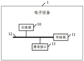
Fig. 7 is a schematic structural diagram of an electronic device for implementing a controllable method for an IPO thickness in an SGT Mosfet according to an embodiment of the present invention.
The electronic device 1 may comprise a processor 10, a memory 11, a bus 12 and a communication interface 13, and may further comprise a computer program stored in the memory 11 and executable on the processor 10, such as a controllable program for IPO thickness in SGT Mosfet.
The memory 11 includes at least one type of readable storage medium, which includes flash memory, removable hard disk, multimedia card, card type memory (e.g., SD or DX memory, etc.), magnetic memory, magnetic disk, optical disk, etc. The memory 11 may in some embodiments be an internal storage unit of the electronic device 1, such as a removable hard disk of the electronic device 1. The memory 11 may also be an external storage device of the electronic device 1 in other embodiments, such as a plug-in mobile hard disk, a Smart Media Card (SMC), a Secure Digital (SD) Card, a Flash memory Card (Flash Card), and the like, which are provided on the electronic device 1. Further, the memory 11 may also include both an internal storage unit and an external storage device of the electronic device 1. The memory 11 can be used not only for storing application software installed in the electronic device 1 and various types of data, such as codes of a controllable program for IPO thickness in SGT Mosfet, etc., but also for temporarily storing data that has been output or is to be output.
The processor 10 may be composed of an integrated circuit in some embodiments, for example, a single packaged integrated circuit, or may be composed of a plurality of integrated circuits packaged with the same or different functions, including one or more Central Processing Units (CPUs), microprocessors, digital Processing chips, graphics processors, and combinations of various control chips. The processor 10 is a Control Unit (Control Unit) of the electronic device, connects various components of the whole electronic device by using various interfaces and lines, and executes various functions and processes data of the electronic device 1 by running or executing programs or modules (e.g., a controllable program of IPO thickness in SGT Mosfet, etc.) stored in the memory 11 and calling data stored in the memory 11.
The bus 12 may be a Peripheral Component Interconnect (PCI) bus, an Extended Industry Standard Architecture (EISA) bus, or the like. The bus 12 may be divided into an address bus, a data bus, a control bus, etc. The bus 12 is arranged to enable connection communication between the memory 11 and at least one processor 10 or the like.
Fig. 7 only shows an electronic device with components, and it will be understood by a person skilled in the art that the structure shown in fig. 7 does not constitute a limitation of the electronic device 1, and may comprise fewer or more components than shown, or a combination of certain components, or a different arrangement of components.
For example, although not shown, the electronic device 1 may further include a power supply (such as a battery) for supplying power to each component, and preferably, the power supply may be logically connected to the at least one processor 10 through a power management device, so as to implement functions of charge management, discharge management, power consumption management, and the like through the power management device. The power supply may also include any component of one or more dc or ac power sources, recharging devices, power failure detection circuitry, power converters or inverters, power status indicators, and the like. The electronic device 1 may further include various sensors, a bluetooth module, a Wi-Fi module, and the like, which are not described herein again.
Further, the electronic device 1 may further include a network interface, and optionally, the network interface may include a wired interface and/or a wireless interface (such as a WI-FI interface, a bluetooth interface, etc.), which are generally used for establishing a communication connection between the electronic device 1 and other electronic devices.
Optionally, the electronic device 1 may further comprise a user interface, which may be a Display (Display), an input unit (such as a Keyboard), and optionally a standard wired interface, a wireless interface. Alternatively, in some embodiments, the display may be an LED display, a liquid crystal display, a touch-sensitive liquid crystal display, an OLED (Organic Light-Emitting Diode) touch device, or the like. The display, which may also be referred to as a display screen or display unit, is suitable for displaying information processed in the electronic device 1 and for displaying a visualized user interface, among other things.
It is to be understood that the described embodiments are for purposes of illustration only and that the scope of the appended claims is not limited to such structures.
The program for controlling IPO thickness in SGT mosfets stored in the memory 11 of the electronic device 1 is a combination of a plurality of instructions, and when running in the processor 10, can implement:
obtaining a silicon trench substrate, and depositing pre-constructed non-doped silicon oxide and source polycrystalline silicon in a trench of the silicon trench substrate to obtain an initial deposition trench;
removing part of the undoped silicon oxide in the initial deposition groove according to a preset depth removal standard to obtain an original to-be-oxidized deposition groove;
implanting nitrogen atoms with preset concentration and energy into the surface of the source electrode polycrystalline silicon in the original to-be-oxidized deposition groove by utilizing pre-constructed nitrogen implantation equipment to obtain a target to-be-oxidized polycrystalline silicon layer;
oxidizing the target polycrystalline silicon layer to be oxidized and the inner wall of the original groove to be oxidized and deposited to obtain an IPO (intrinsic polycrystalline silicon) oxide layer with the target thickness and a grid oxide layer with the target thickness respectively;
and depositing pre-constructed grid polysilicon on the surfaces of the target thickness IPO oxide layer and the target thickness grid oxide layer to finish the regulation and control of the IPO thickness.
Specifically, the specific implementation method of the processor 10 for the instruction may refer to the description of the relevant steps in the embodiments corresponding to fig. 1 to fig. 6, which is not repeated herein.
Further, the integrated modules/units of the electronic device 1 may be stored in a computer-readable storage medium if they are implemented in the form of software functional units and sold or used as separate products. The computer readable storage medium may be volatile or non-volatile. For example, the computer-readable medium may include: any entity or device capable of carrying said computer program code, recording medium, U-disk, removable hard disk, magnetic disk, optical disk, computer Memory, Read-Only Memory (ROM).
The present invention also provides a computer-readable storage medium, storing a computer program which, when executed by a processor of an electronic device, may implement:
obtaining a silicon trench substrate, and depositing pre-constructed non-doped silicon oxide and source polycrystalline silicon in a trench of the silicon trench substrate to obtain an initial deposition trench;
removing part of the undoped silicon oxide in the initial deposition groove according to a preset depth removal standard to obtain an original to-be-oxidized deposition groove;
implanting nitrogen atoms with preset concentration and energy into the surface of the source electrode polycrystalline silicon in the original to-be-oxidized deposition groove by utilizing pre-constructed nitrogen implantation equipment to obtain a target to-be-oxidized polycrystalline silicon layer;
oxidizing the target polycrystalline silicon layer to be oxidized and the inner wall of the original groove to be oxidized and deposited to obtain an IPO (intrinsic polycrystalline silicon) oxide layer with a target thickness and a grid oxide layer with a target thickness respectively;
and depositing pre-constructed grid polysilicon on the surfaces of the target thickness IPO oxide layer and the target thickness grid oxide layer to finish the regulation and control of the IPO thickness.
In the embodiments provided in the present invention, it should be understood that the disclosed apparatus, device and method can be implemented in other ways. For example, the above-described apparatus embodiments are merely illustrative, and for example, the division of the modules is only one logical functional division, and other divisions may be realized in practice.
The modules described as separate parts may or may not be physically separate, and parts displayed as modules may or may not be physical units, may be located in one place, or may be distributed on a plurality of network units. Some or all of the modules may be selected according to actual needs to achieve the purpose of the solution of the present embodiment.
In addition, functional modules in the embodiments of the present invention may be integrated into one processing unit, or each unit may exist alone physically, or two or more units are integrated into one unit. The integrated unit can be realized in a form of hardware, or in a form of hardware plus a software functional module.
It will be evident to those skilled in the art that the invention is not limited to the details of the foregoing illustrative embodiments, and that the present invention may be embodied in other specific forms without departing from the spirit or essential attributes thereof.
The present embodiments are therefore to be considered in all respects as illustrative and not restrictive, the scope of the invention being indicated by the appended claims rather than by the foregoing description, and all changes which come within the meaning and range of equivalency of the claims are therefore intended to be embraced therein. Any reference signs in the claims shall not be construed as limiting the claim concerned.
The block chain is a novel application mode of computer technologies such as distributed data storage, point-to-point transmission, a consensus mechanism, an encryption algorithm and the like. A block chain (Blockchain), which is essentially a decentralized database, is a series of data blocks associated by using a cryptographic method, and each data block contains information of a batch of network transactions, so as to verify the validity (anti-counterfeiting) of the information and generate a next block. The blockchain may include a blockchain underlying platform, a platform product service layer, an application service layer, and the like.
Furthermore, it will be obvious that the term "comprising" does not exclude other elements or steps, and the singular does not exclude the plural. A plurality of units or means recited in the system claims may also be implemented by one unit or means in software or hardware. The terms second, etc. are used to denote names, but not any particular order.
Finally, it should be noted that the above embodiments are only for illustrating the technical solutions of the present invention and not for limiting, and although the present invention is described in detail with reference to the preferred embodiments, it should be understood by those skilled in the art that modifications or equivalent substitutions may be made on the technical solutions of the present invention without departing from the spirit and scope of the technical solutions of the present invention.