Detailed Description
The following embodiments of the present invention are provided by way of specific examples, and other advantages and effects of the present invention will be readily apparent to those skilled in the art from the disclosure herein. The invention is capable of other and different embodiments and of being practiced or of being carried out in various ways, and its several details are capable of modification in various respects, all without departing from the spirit and scope of the present invention.
The following examples and comparative examples are parallel runs, with the same processing steps and parameters, unless otherwise indicated.
Example 1
An angle control method in a semiconductor Lift off process comprises the following steps:
s1, depositing silicon dioxide on the surface of the substrate;
s2, coating a positive photoresist on the silicon dioxide surface of the obtained device;
s3, exposing the positive photoresist after the positive photoresist surface of the obtained device shields the graphical mask plate;
s4, developing the positive photoresist, and removing the exposed positive photoresist;
s5, etching the silicon dioxide layer of the obtained device by adopting wet etching to form an etching pattern which is the same as that of the photoresist layer;
s6, depositing a metal layer on the surface of the obtained device;
s7, stripping the silicon dioxide layer on the surface of the device, the positive photoresist layer and the metal layer on the surface of the positive photoresist layer.
S1, depositing the silicon dioxide, wherein the temperature is 250 ℃, Ar (argon) is introduced, the flow is 800sccm, and the working pressure is 0.2 Pa;
and S1, performing programmed heating treatment after the silicon dioxide is deposited.
The above-mentioned programmed heating treatment comprises: 300 ℃ for 10s, 550 ℃ for 10s, and 400 ℃ for 10 s.
S3 further includes heating to 100 deg.C for 30S after exposure.
S3, the exposure time of the ultraviolet light is 60S, the wavelength of the ultraviolet light is 300-400nm, and the power is 12-17mW/cm 2 。
S4, the developing solution comprises 0.8 wt% sodium hydroxide solution.
S4, the developing method comprises the following steps: spraying excessive developing solution on the surface of the positive photoresist to enable the developing solution to be fully distributed on the surface of the whole positive photoresist, and standing for 90s to enable the positive photoresist in the positive photoresist dissoluble area to be dissolved; continuously spraying the developing solution and simultaneously rotating the device at a speed of 50rpm/min for 30 s; continuously spraying excessive developing solution to make the developing solution fully spread on the surface of the whole positive photoresist, standing for 60s, and rotating the device at the speed of 100rpm/min to throw out the developing solution dissolved with the positive photoresist and the redundant developing solution; and spraying deionized water to the positive photoresist, rotating the device at the speed of 100rpm/min for spin-drying, and repeatedly spraying deionized water and spin-drying for 2 times to clean the device.
S4 further comprises heating at 130 deg.C for 30S after development.
The developing solution can be replaced by other commercially available or published positive photoresist developing solutions, and the developing method can be adjusted accordingly.
And S5, performing wet etching, wherein the etching liquid comprises hydrofluoric acid solution.
S5, the hydrofluoric acid solution comprises deionized water and hydrofluoric acid, and the volume ratio of the deionized water to the hydrofluoric acid is 12: 1.
S5, etching, including: immersing the obtained device in hydrofluoric acid solution, standing for 40min, taking out, and repeating the steps for 5 times; and washing with deionized water and drying (spin-drying).
S6 the deposited metal comprises Ag.
The metal layer deposited in S6 was 110nm thick.
S1 the silicon dioxide is deposited to a thickness of 200 nm.
S2 the coating thickness of the positive photoresist is 1.7 μm.
S7, adopting a method of independently stripping a deposited metal layer: and adhering the adhesive with strong adhesion to the surface of the metal layer on the surface of the positive photoresist layer, tearing the adhesive to peel off the metal layer on the surface of the positive photoresist layer, and peeling off the residual positive photoresist layer and the silicon dioxide layer.
The stripping method of the positive photoresist layer and the silicon dioxide layer can adopt a stripping liquid to ultrasonically assist stripping, wherein the stripping liquid comprises hydrofluoric acid with the volume percentage of 30% vol.
Example 2
An angle control method in a semiconductor Lift off process comprises the following steps:
s1, depositing silicon dioxide on the surface of the substrate;
s2, coating a positive photoresist on the silicon dioxide surface of the obtained device;
s3, exposing the positive photoresist after the positive photoresist surface of the obtained device shields the graphical mask plate;
s4, developing the positive photoresist, and removing the positive photoresist at the exposed part;
s5, etching the silicon dioxide layer of the obtained device by wet etching to form an etching pattern which is the same as the photoresist layer on the silicon dioxide layer;
s6, depositing a metal layer on the surface of the obtained device;
s7, stripping the silicon dioxide layer on the surface of the device, the positive photoresist layer and the metal layer on the surface of the positive photoresist layer.
S1, depositing the silicon dioxide, wherein the temperature is 330 ℃, Ar (argon) is introduced, the flow is 1000sccm, and the working pressure is 0.3 Pa;
and S1, performing programmed heating treatment after the silicon dioxide is deposited.
The above-mentioned programmed heating treatment comprises: 300 ℃ for 10s, 550 ℃ for 10s, and 400 ℃ for 10 s.
S3 further includes heating to 100 deg.C for 30S after exposure.
S3, the exposure time of the ultraviolet light is 60S, the wavelength of the ultraviolet light is 300-400nm, and the power is 12-17mW/cm 2 。
S4, the developing solution comprises 0.8 wt% sodium hydroxide solution.
And S4, developing in a developer solution in a mode of spin-coating immersion: spraying excessive developing solution on the surface of the positive photoresist to enable the developing solution to be fully distributed on the surface of the whole positive photoresist, and standing for 90s to enable the positive photoresist in the positive photoresist dissoluble area to be dissolved; continuously spraying the developing solution and simultaneously rotating the device at a speed of 50rpm/min for 30 s; continuously spraying excessive developing solution to make the developing solution fully spread on the surface of the whole positive photoresist, standing for 60s, and rotating the device at the speed of 100rpm/min to throw out the developing solution dissolved with the positive photoresist and the redundant developing solution; and spraying deionized water to the positive photoresist, rotating the device at the speed of 100rpm/min for spin-drying, and repeatedly spraying deionized water and spin-drying for 2 times to clean the device.
S4 further comprises, after developing, heating at 130 ℃ for 30S.
The developing solution can be replaced by other commercially available or disclosed positive photoresist developing solutions, and the developing method can be adjusted accordingly.
And S5, performing wet etching, wherein the etching liquid comprises hydrofluoric acid solution.
S5, the hydrofluoric acid solution comprises deionized water and hydrofluoric acid, and the volume ratio of the deionized water to the hydrofluoric acid is 10:1.
S5, etching, including: immersing the obtained device in hydrofluoric acid solution, standing for 40min, taking out, and repeating the steps for 5 times; and washing with deionized water and drying (spin-drying).
S6 the deposited metal comprises Ag.
The metal layer deposited in S6 was 110nm thick.
S1 the silicon dioxide is deposited to a thickness of 130 nm.
S2 the coating thickness of the positive photoresist is 1.4 μm.
S7, stripping, namely, adopting a method of separately stripping the deposited metal layer: and adhering the adhesive with strong adhesion to the surface of the metal layer on the surface of the positive photoresist layer, tearing the adhesive to peel off the metal layer on the surface of the positive photoresist layer, and peeling off the residual positive photoresist layer and the silicon dioxide layer.
The stripping method of the positive photoresist layer and the silicon dioxide layer can adopt a stripping liquid to ultrasonically assist stripping, wherein the stripping liquid comprises hydrofluoric acid with the volume percentage of 30% vol.
Example 3
An angle control method in a semiconductor Lift off process comprises the following steps:
s1, depositing silicon dioxide on the surface of the substrate;
s2, coating a positive photoresist on the silicon dioxide surface of the obtained device;
s3, exposing the positive photoresist after the positive photoresist surface of the obtained device shields the graphical mask plate;
s4, developing the positive photoresist, and removing the positive photoresist at the exposed part;
s5, etching the silicon dioxide layer of the obtained device by adopting wet etching to form an etching pattern which is the same as that of the photoresist layer;
s6, depositing a metal layer on the surface of the obtained device;
s7, stripping the silicon dioxide layer on the surface of the device, the positive photoresist layer and the metal layer on the surface of the positive photoresist layer.
S1, depositing the silicon dioxide, wherein the temperature is 300 ℃, Ar (argon) is introduced, the flow is 1000sccm, and the working pressure is 0.2 Pa;
and S1, performing programmed heating treatment after the silicon dioxide is deposited.
The above-mentioned programmed heating treatment comprises: 300 ℃ for 10s, 550 ℃ for 10s, and 400 ℃ for 10 s.
S3 further includes heating to 100 deg.C for 30S after exposure.
S3, the exposure time of the ultraviolet light is 60S, the wavelength of the ultraviolet light is 300-400nm, and the power is 12-17mW/cm 2 。
S4, the developing solution comprises 0.8 wt% sodium hydroxide solution.
And S4, developing in a developer solution in a mode of spin-coating immersion: spraying excessive developing solution on the surface of the positive photoresist to enable the developing solution to be fully distributed on the surface of the whole positive photoresist, and standing for 90s to enable the positive photoresist in the positive photoresist dissoluble area to be dissolved; continuously spraying the developing solution and simultaneously rotating the device at a speed of 50rpm/min for 30 s; continuously spraying excessive developing solution to make the developing solution fully spread on the surface of the whole positive photoresist, standing for 60s, and rotating the device at the speed of 100rpm/min to throw out the developing solution dissolved with the positive photoresist and the redundant developing solution; and spraying deionized water to the positive photoresist, rotating the device at the speed of 100rpm/min for spin-drying, and repeatedly spraying deionized water and spin-drying for 2 times to clean the device.
S4 further comprises heating at 130 deg.C for 30S after development.
The developing solution can be replaced by other commercially available or disclosed positive photoresist developing solutions, and the developing method can be adjusted accordingly.
And S5, performing wet etching, wherein the etching liquid comprises hydrofluoric acid solution.
S5, the hydrofluoric acid solution comprises deionized water and hydrofluoric acid, and the volume ratio of the deionized water to the hydrofluoric acid is 10:1.
S5, etching, including: immersing the obtained device in hydrofluoric acid solution, standing for 40min, taking out, and repeating the steps for 5 times; and washing with deionized water and drying (spin-drying).
S6 the deposited metal comprises Ag.
The metal layer deposited in S6 was 110nm thick.
S1 the silicon dioxide is deposited to a thickness of 130 nm.
S2 the coating thickness of the positive photoresist is 1.4 μm.
S7, stripping, namely, adopting a method of separately stripping the deposited metal layer: and adhering the adhesive with strong adhesion to the surface of the metal layer on the surface of the positive photoresist layer, tearing the adhesive to peel off the metal layer on the surface of the positive photoresist layer, and peeling off the residual positive photoresist layer and the silicon dioxide layer.
The stripping method of the positive photoresist layer and the silicon dioxide layer can adopt a stripping liquid to ultrasonically assist stripping, wherein the stripping liquid comprises hydrofluoric acid with the volume percentage of 30% vol.
Example 4
An angle control method in a semiconductor Lift off process comprises the following steps:
s1, depositing silicon dioxide on the surface of the substrate;
s2, coating a positive photoresist on the silicon dioxide surface of the obtained device;
s3, exposing the positive photoresist after the positive photoresist surface of the obtained device shields the graphical mask plate;
s4, developing the positive photoresist, and removing the positive photoresist at the exposed part;
s5, etching the silicon dioxide layer of the obtained device by wet etching to form an etching pattern which is the same as the photoresist layer on the silicon dioxide layer;
s6, depositing a metal layer on the surface of the obtained device;
s7, stripping the silicon dioxide layer on the surface of the device, the positive photoresist layer and the metal layer on the surface of the positive photoresist layer.
S1, depositing the silicon dioxide, wherein the temperature is 300 ℃, Ar (argon) is introduced, the flow is 1000sccm, and the working pressure is 0.2 Pa;
and S1, performing programmed heating treatment after the silicon dioxide is deposited.
The above-mentioned programmed heating treatment comprises: 300 ℃ for 10s, 550 ℃ for 10s, and 400 ℃ for 10 s.
S3 further includes heating to 100 deg.C for 30S after exposure.
S3, the exposure time of the ultraviolet light is 60S, and the wavelength of the ultraviolet light is 300-400nm, power of 12-17mW/cm 2 。
S4, the developing solution comprises 0.8 wt% sodium hydroxide solution.
And S4, developing in a developer solution in a mode of spin-coating immersion: spraying excessive developing solution on the surface of the positive photoresist to enable the developing solution to be fully distributed on the surface of the whole positive photoresist, and standing for 90s to enable the positive photoresist in the positive photoresist dissoluble area to be dissolved; continuously spraying the developing solution and simultaneously rotating the device at a speed of 50rpm/min for 30 s; continuously spraying excessive developing solution to make the developing solution fully spread on the surface of the whole positive photoresist, standing for 60s, and rotating the device at the speed of 100rpm/min to throw out the developing solution dissolved with the positive photoresist and the redundant developing solution; and spraying deionized water to the positive photoresist, rotating the device at the speed of 100rpm/min for spin-drying, and repeatedly spraying deionized water and spin-drying for 2 times to clean the device.
S4 further comprises heating at 130 deg.C for 30S after development.
The developing solution can be replaced by other commercially available or disclosed positive photoresist developing solutions, and the developing method can be adjusted accordingly.
And S5, performing wet etching, wherein the etching liquid comprises hydrofluoric acid solution.
S5, the hydrofluoric acid solution comprises deionized water and hydrofluoric acid, and the volume ratio of the deionized water to the hydrofluoric acid is 10:1.
S5, etching, including: immersing the obtained device in hydrofluoric acid solution, standing for 40min, performing ultrasound for 3min, and repeating the steps of standing and ultrasound for 5 times; and washing with deionized water and drying (spin-drying).
S6 the deposited metal comprises Ag.
The metal layer deposited in S6 was 110nm thick.
S1 the silicon dioxide is deposited to a thickness of 130 nm.
S2 the coating thickness of the positive photoresist is 1.4 μm.
S7, stripping, namely, adopting a method of separately stripping the deposited metal layer: and adhering the adhesive with strong adhesion to the surface of the metal layer on the surface of the positive photoresist layer, tearing the adhesive to peel off the metal layer on the surface of the positive photoresist layer, and peeling off the residual positive photoresist layer and the silicon dioxide layer.
The stripping method of the positive photoresist layer and the silicon dioxide layer can adopt a stripping liquid to ultrasonically assist stripping, wherein the stripping liquid comprises hydrofluoric acid with the volume percentage of 30% vol.
Example 5
An angle control method in a semiconductor Lift off process comprises the following steps:
s1, depositing silicon dioxide on the surface of the substrate;
s2, coating a positive photoresist on the silicon dioxide surface of the obtained device;
s3, exposing the positive photoresist after the positive photoresist surface of the obtained device shields the graphical mask plate;
s4, developing the positive photoresist, and removing the positive photoresist at the exposed part;
s5, etching the silicon dioxide layer of the obtained device by wet etching to form an etching pattern which is the same as the photoresist layer on the silicon dioxide layer;
s6, depositing a metal layer on the surface of the obtained device;
s7, stripping the silicon dioxide layer on the surface of the device, the positive photoresist layer and the metal layer on the surface of the positive photoresist layer.
S1, depositing the silicon dioxide, wherein the temperature is 300 ℃, Ar (argon) is introduced, the flow is 1000sccm, and the working pressure is 0.2 Pa;
and S1, performing programmed heating treatment after the silicon dioxide is deposited.
The above-mentioned programmed heating treatment comprises: 300 ℃ for 10s, 550 ℃ for 10s, and 400 ℃ for 10 s.
S3 further includes heating to 100 deg.C for 30S after exposure.
S3, the exposure time of the ultraviolet light is 60S, the wavelength of the ultraviolet light is 300-400nm, and the power is 12-17mW/cm 2 。
S4, the developing solution comprises 0.8 wt% sodium hydroxide solution.
And S4, developing in a developer solution in a mode of spin-coating immersion: spraying excessive developing solution on the surface of the positive photoresist to enable the developing solution to be fully distributed on the surface of the whole positive photoresist, and standing for 90s to enable the positive photoresist in the positive photoresist dissoluble area to be dissolved; continuously spraying the developing solution and simultaneously rotating the device at a speed of 50rpm/min for 30 s; continuously spraying excessive developing solution to make the developing solution fully spread on the surface of the whole positive photoresist, standing for 60s, and rotating the device at the speed of 100rpm/min to throw out the developing solution dissolved with the positive photoresist and the redundant developing solution; and spraying deionized water to the positive photoresist, rotating the device at the speed of 100rpm/min for spin-drying, and repeatedly spraying deionized water and spin-drying for 2 times to clean the device.
S4 further comprises heating at 130 deg.C for 30S after development.
The developing solution can be replaced by other commercially available or disclosed positive photoresist developing solutions, and the developing method can be adjusted accordingly.
And S5, performing wet etching, wherein the etching liquid comprises hydrofluoric acid solution.
S5, the hydrofluoric acid solution comprises deionized water and hydrofluoric acid, and the volume ratio of the deionized water to the hydrofluoric acid is 10:1.
S5, etching, including: immersing the obtained device in hydrofluoric acid solution, standing for 40min, performing ultrasound for 3min, and repeating the standing and ultrasound steps for 5 times; and washing with deionized water and drying (spin-drying).
S6 the deposited metal comprises Ag.
The metal layer deposited in S6 was 110nm thick.
S1 the silicon dioxide is deposited to a thickness of 130 nm.
The thickness of the positive photoresist layer is set to
Is deposited byThe metal layer has a thickness of
Then, then
This example takes
,
Is 1540 nm.
S7, stripping, namely, adopting a method of separately stripping the deposited metal layer: and adhering the adhesive with strong adhesion to the surface of the metal layer on the surface of the positive photoresist layer, tearing the adhesive to peel off the metal layer on the surface of the positive photoresist layer, and peeling off the residual positive photoresist layer and the silicon dioxide layer.
The stripping method of the positive photoresist layer and the silicon dioxide layer can adopt a stripping liquid to ultrasonically assist stripping, wherein the stripping liquid comprises hydrofluoric acid with the volume percentage of 30% vol.
Example 6
An angle control method in a semiconductor Lift off process comprises the following steps:
s1, depositing silicon dioxide on the surface of the substrate;
s2, coating a positive photoresist on the silicon dioxide surface of the obtained device;
s3, exposing the positive photoresist after the positive photoresist surface of the obtained device shields the graphical mask plate;
s4, developing the positive photoresist, and removing the positive photoresist at the exposed part;
s5, etching the silicon dioxide layer of the obtained device by wet etching to form an etching pattern which is the same as the photoresist layer on the silicon dioxide layer;
s6, depositing a metal layer on the surface of the obtained device;
s7, stripping the silicon dioxide layer on the surface of the device, the positive photoresist layer and the metal layer on the surface of the positive photoresist layer.
S1, depositing the silicon dioxide, wherein the temperature is 300 ℃, Ar (argon) is introduced, the flow is 1000sccm, and the working pressure is 0.2 Pa;
and S1, performing programmed heating treatment after the silicon dioxide is deposited.
The above-mentioned programmed heating treatment comprises: 300 ℃ for 10s, 550 ℃ for 10s, and 400 ℃ for 10 s.
S3 further includes heating to 100 deg.C for 30S after exposure.
S3, the exposure time of the ultraviolet light is 60S, the wavelength of the ultraviolet light is 300-400nm, and the power is 12-17mW/cm 2 。
S4, the developing solution comprises 0.8 wt% sodium hydroxide solution.
And S4, developing in a developer solution in a mode of spin-coating immersion: spraying excessive developing solution on the surface of the positive photoresist to enable the developing solution to be fully distributed on the surface of the whole positive photoresist, and standing for 90s to enable the positive photoresist in the positive photoresist dissoluble area to be dissolved; continuously spraying the developing solution and simultaneously rotating the device at a speed of 50rpm/min for 30 s; continuously spraying excessive developing solution to make the developing solution fully spread on the surface of the whole positive photoresist, standing for 60s, and rotating the device at the speed of 100rpm/min to throw out the developing solution dissolved with the positive photoresist and the redundant developing solution; and spraying deionized water to the positive photoresist, rotating the device at the speed of 100rpm/min for spin-drying, and repeatedly spraying deionized water and spin-drying for 2 times to clean the device.
S4 further comprises heating at 130 deg.C for 30S after development.
The developing solution can be replaced by other commercially available or disclosed positive photoresist developing solutions, and the developing method can be adjusted accordingly.
And S5, performing wet etching, wherein the etching liquid comprises hydrofluoric acid solution.
S5, the hydrofluoric acid solution comprises deionized water and hydrofluoric acid, and the volume ratio of the deionized water to the hydrofluoric acid is 10:1.
S5, etching, including: immersing the obtained device in hydrofluoric acid solution, standing for 40min, performing ultrasound for 3min, and repeating the steps of standing and ultrasound for 5 times; and washing with deionized water and drying (spin-drying).
S6 the deposited metal comprises Ag.
The metal layer deposited in S6 was 110nm thick.
S1 the silicon dioxide is deposited to a thickness of 130 nm.
Setting the thickness of the positive photoresist layer as
The thickness of the deposited metal layer is
Then, then
This example takes
,
Was 1650 nm.
S7, adopting a method of independently stripping a deposited metal layer: and adopting the adhesive with strong adhesive force to adhere to the surface of the metal layer on the surface of the positive photoresist layer, tearing the adhesive to peel off the metal layer on the surface of the positive photoresist layer, and peeling off the residual positive photoresist layer and the silicon dioxide layer additionally.
The stripping method of the positive photoresist layer and the silicon dioxide layer can adopt a stripping liquid to ultrasonically assist stripping, wherein the stripping liquid comprises hydrofluoric acid with the volume percentage of 30% vol.
Example 7
An angle control method in a semiconductor Lift off process comprises the following steps:
s1, depositing silicon dioxide on the surface of the substrate;
s2, coating a positive photoresist on the silicon dioxide surface of the obtained device;
s3, exposing the positive photoresist after the positive photoresist surface of the obtained device shields the graphical mask plate;
s4, developing the positive photoresist, and removing the positive photoresist at the exposed part;
s5, etching the silicon dioxide layer of the obtained device by wet etching to form an etching pattern which is the same as the photoresist layer on the silicon dioxide layer;
s6, depositing a metal layer on the surface of the obtained device;
s7, stripping the silicon dioxide layer on the surface of the device, the positive photoresist layer and the metal layer on the surface of the positive photoresist layer.
S1, depositing the silicon dioxide, wherein the temperature is 300 ℃, Ar (argon) is introduced, the flow is 1000sccm, and the working pressure is 0.2 Pa;
and S1, performing programmed heating treatment after the silicon dioxide is deposited.
The above-mentioned programmed heating treatment comprises: 300 ℃ for 10s, 550 ℃ for 10s, and 400 ℃ for 10 s.
S3 further includes heating to 100 deg.C for 30S after exposure.
S3, the exposure time of the ultraviolet light is 60S, the wavelength of the ultraviolet light is 300-400nm, and the power is 12-17mW/cm 2 。
S4, the developing solution comprises 0.8 wt% sodium hydroxide solution.
And S4, developing in a developer solution in a mode of spin-coating immersion: spraying excessive developing solution on the surface of the positive photoresist to enable the developing solution to be fully distributed on the surface of the whole positive photoresist, and standing for 90s to enable the positive photoresist in the positive photoresist dissoluble area to be dissolved; continuously spraying the developing solution and simultaneously rotating the device at a speed of 50rpm/min for 30 s; continuously spraying excessive developing solution to make the developing solution fully spread on the surface of the whole positive photoresist, standing for 60s, and rotating the device at the speed of 100rpm/min to throw out the developing solution dissolved with the positive photoresist and the redundant developing solution; and spraying deionized water to the positive photoresist, rotating the device at the speed of 100rpm/min for spin-drying, and repeatedly spraying deionized water and spin-drying for 2 times to clean the device.
S4 further comprises heating at 130 deg.C for 30S after development.
The developing solution can be replaced by other commercially available or published positive photoresist developing solutions, and the developing method can be adjusted accordingly.
And S5, performing wet etching, wherein the etching liquid comprises hydrofluoric acid solution.
S5, the hydrofluoric acid solution comprises deionized water and hydrofluoric acid, and the volume ratio of the deionized water to the hydrofluoric acid is 10:1.
S5, etching, including: immersing the obtained device in hydrofluoric acid solution, standing for 40min, performing ultrasound for 3min, and repeating the standing and ultrasound steps for 5 times; and washing with deionized water and drying (spin-drying).
S6 the deposited metal comprises Ag.
The metal layer deposited in S6 was 110nm thick.
S2 the coating thickness of the positive photoresist is 1.4 μm.
Let the thickness of the silicon dioxide layer be
S6 obtaining a deposited metal layer having a thickness of
Then, then
This example takes
,
Was 143 nm.
S7, stripping, namely, adopting a method of separately stripping the deposited metal layer: and adhering the adhesive with strong adhesion to the surface of the metal layer on the surface of the positive photoresist layer, tearing the adhesive to peel off the metal layer on the surface of the positive photoresist layer, and peeling off the residual positive photoresist layer and the silicon dioxide layer.
The stripping method of the positive photoresist layer and the silicon dioxide layer can adopt a stripping liquid to ultrasonically assist stripping, wherein the stripping liquid comprises hydrofluoric acid with the volume percentage of 30% vol.
Example 8
An angle control method in a semiconductor Lift off process comprises the following steps:
s1, depositing silicon dioxide on the surface of the substrate;
s2, coating a positive photoresist on the silicon dioxide surface of the obtained device;
s3, exposing the positive photoresist after the positive photoresist surface of the obtained device shields the graphical mask plate;
s4, developing the positive photoresist, and removing the positive photoresist at the exposed part;
s5, etching the silicon dioxide layer of the obtained device by wet etching to form an etching pattern which is the same as the photoresist layer on the silicon dioxide layer;
s6, depositing a metal layer on the surface of the obtained device;
s7, stripping the silicon dioxide layer on the surface of the device, the positive photoresist layer and the metal layer on the surface of the positive photoresist layer.
S1, depositing the silicon dioxide, wherein the temperature is 300 ℃, Ar (argon) is introduced, the flow is 1000sccm, and the working pressure is 0.2 Pa;
and S1, performing programmed heating treatment after the silicon dioxide is deposited.
The above-mentioned programmed heating treatment comprises: 300 ℃ for 10s, 550 ℃ for 10s, and 400 ℃ for 10 s.
S3 further includes heating to 100 deg.C for 30S after exposure.
S3, the exposure time of the ultraviolet light is 60S, the wavelength of the ultraviolet light is 300-400nm, and the power is 12-17mW/cm 2 。
S4, the developing solution comprises 0.8 wt% sodium hydroxide solution.
And S4, developing in a developer solution in a mode of spin-coating immersion: spraying excessive developing solution on the surface of the positive photoresist to enable the developing solution to be fully distributed on the surface of the whole positive photoresist, and standing for 90s to enable the positive photoresist in the positive photoresist dissoluble area to be dissolved; continuously spraying the developing solution and simultaneously rotating the device at a speed of 50rpm/min for 30 s; continuously spraying excessive developing solution to make the developing solution fully spread on the surface of the whole positive photoresist, standing for 60s, and rotating the device at the speed of 100rpm/min to throw out the developing solution dissolved with the positive photoresist and the redundant developing solution; and spraying deionized water to the positive photoresist, rotating the device at the speed of 100rpm/min for spin-drying, and repeatedly spraying deionized water and spin-drying for 2 times to clean the device.
S4 further comprises heating at 130 deg.C for 30S after development.
The developing solution can be replaced by other commercially available or disclosed positive photoresist developing solutions, and the developing method can be adjusted accordingly.
And S5, performing wet etching, wherein the etching liquid comprises hydrofluoric acid solution.
S5, the hydrofluoric acid solution comprises deionized water and hydrofluoric acid, and the volume ratio of the deionized water to the hydrofluoric acid is 10:1.
S5, etching, including: immersing the obtained device in hydrofluoric acid solution, standing for 40min, performing ultrasound for 3min, and repeating the steps of standing and ultrasound for 5 times; and washing with deionized water and drying (spin-drying).
S6 the deposited metal comprises Ag.
The metal layer deposited in S6 was 110nm thick.
S2 the coating thickness of the positive photoresist is 1.4 μm.
Let the thickness of the silicon dioxide layer be
S6 obtaining a deposited metal layer having a thickness of
Then, then
This example takes
,
Is 187 nm.
S7, stripping, namely, adopting a method of separately stripping the deposited metal layer: and adhering the adhesive with strong adhesion to the surface of the metal layer on the surface of the positive photoresist layer, tearing the adhesive to peel off the metal layer on the surface of the positive photoresist layer, and peeling off the residual positive photoresist layer and the silicon dioxide layer.
The stripping method of the positive photoresist layer and the silicon dioxide layer can adopt a stripping liquid to ultrasonically assist stripping, wherein the stripping liquid comprises hydrofluoric acid with the volume percentage of 30% vol.
Example 9
An angle control method in a semiconductor Lift off process comprises the following steps:
s1, depositing silicon dioxide on the surface of the substrate;
s2, coating a positive photoresist on the silicon dioxide surface of the obtained device;
s3, exposing the positive photoresist after the positive photoresist surface of the obtained device shields the graphical mask plate;
s4, developing the positive photoresist, and removing the positive photoresist at the exposed part;
s5, etching the silicon dioxide layer of the obtained device by adopting wet etching to form an etching pattern which is the same as that of the photoresist layer;
s6, depositing a metal layer on the surface of the obtained device;
s7, stripping the silicon dioxide layer on the surface of the device, the positive photoresist layer and the metal layer on the surface of the positive photoresist layer.
S1, depositing the silicon dioxide, wherein the temperature is 300 ℃, Ar (argon) is introduced, the flow is 1000sccm, and the working pressure is 0.2 Pa;
s1, after the silicon dioxide is deposited, carrying out programmed heating treatment.
The above-mentioned programmed heating treatment comprises: 300 ℃ for 10s, 550 ℃ for 10s, and 400 ℃ for 10 s.
S3 further includes heating to 100 deg.C for 30S after exposure.
S3, the exposure time of the ultraviolet light is 60S, the wavelength of the ultraviolet light is 300-400nm, and the power is 12-17mW/cm 2 。
S4, the developing solution comprises 0.8 wt% sodium hydroxide solution.
And S4, developing in a developer solution in a mode of spin-coating immersion: spraying excessive developing solution on the surface of the positive photoresist to enable the developing solution to be fully distributed on the surface of the whole positive photoresist, and standing for 90s to enable the positive photoresist in the positive photoresist dissoluble area to be dissolved; continuously spraying the developing solution and simultaneously rotating the device at a speed of 50rpm/min for 30 s; continuously spraying excessive developing solution to make the developing solution fully spread on the surface of the whole positive photoresist, standing for 60s, and rotating the device at the speed of 100rpm/min to throw out the developing solution dissolved with the positive photoresist and the redundant developing solution; and spraying deionized water to the positive photoresist, rotating the device at the speed of 100rpm/min for spin-drying, and repeatedly spraying deionized water and spin-drying for 2 times to clean the device.
S4 further comprises heating at 130 deg.C for 30S after development.
The developing solution can be replaced by other commercially available or disclosed positive photoresist developing solutions, and the developing method can be adjusted accordingly.
And S5, performing wet etching, wherein the etching liquid comprises hydrofluoric acid solution.
S5, the hydrofluoric acid solution comprises deionized water and hydrofluoric acid, and the volume ratio of the deionized water to the hydrofluoric acid is 10:1.
S5, etching, including: immersing the obtained device in hydrofluoric acid solution, standing for 40min, performing ultrasound for 3min, and repeating the standing and ultrasound steps for 5 times; and washing with deionized water and drying (spin-drying).
S6 the deposited metal comprises Ag.
The metal layer deposited in S6 was 110nm thick.
Let the thickness of the silicon dioxide layer be
S6 obtaining a deposited metal layer having a thickness of
Then, then
This example takes
,
Is 143 nm.
The thickness of the positive photoresist layer is set to
The thickness of the deposited metal layer is
Then, then
This example takes
,
Is 1540 nm.
S7, stripping, namely, adopting a method of separately stripping the deposited metal layer: and adhering the adhesive with strong adhesion to the surface of the metal layer on the surface of the positive photoresist layer, tearing the adhesive to peel off the metal layer on the surface of the positive photoresist layer, and peeling off the residual positive photoresist layer and the silicon dioxide layer.
The stripping method of the positive photoresist layer and the silicon dioxide layer can adopt a stripping liquid to ultrasonically assist stripping, wherein the stripping liquid comprises hydrofluoric acid with the volume percentage of 30% vol.
Example 10
An angle control method in a semiconductor Lift off process comprises the following steps:
s1, depositing silicon dioxide on the surface of the substrate;
s2, coating a positive photoresist on the silicon dioxide surface of the obtained device;
s3, exposing the positive photoresist after the positive photoresist surface of the obtained device shields the graphical mask plate;
s4, developing the positive photoresist, and removing the positive photoresist at the exposed part;
s5, etching the silicon dioxide layer of the obtained device by wet etching to form an etching pattern which is the same as the photoresist layer on the silicon dioxide layer;
s6, depositing a metal layer on the surface of the obtained device;
s7, stripping the silicon dioxide layer on the surface of the device, the positive photoresist layer and the metal layer on the surface of the positive photoresist layer.
S1, depositing the silicon dioxide, wherein the temperature is 300 ℃, Ar (argon) is introduced, the flow is 1000sccm, and the working pressure is 0.2 Pa;
and S1, performing programmed heating treatment after the silicon dioxide is deposited.
The above-mentioned programmed heating treatment comprises: 300 ℃ for 10s, 550 ℃ for 10s, and 400 ℃ for 10 s.
S3 further includes heating to 100 deg.C for 30S after exposure.
S3, the exposure time of the ultraviolet light is 60S, the wavelength of the ultraviolet light is 300-400nm, and the power is 12-17mW/cm 2 。
S4, the developing solution comprises 0.8 wt% sodium hydroxide solution.
S4, the developing method comprises the following steps: spraying excessive developing solution on the surface of the positive photoresist to enable the developing solution to be fully distributed on the surface of the whole positive photoresist, and standing for 90s to enable the positive photoresist in the positive photoresist dissoluble area to be dissolved; continuously spraying the developing solution and simultaneously rotating the device at a speed of 50rpm/min for 30 s; continuously spraying excessive developing solution to make the developing solution fully spread on the surface of the whole positive photoresist, standing for 60s, and rotating the device at the speed of 100rpm/min to throw out the developing solution dissolved with the positive photoresist and the redundant developing solution; and spraying deionized water to the positive photoresist, rotating the device at the speed of 100rpm/min for spin-drying, and repeatedly spraying deionized water and spin-drying for 2 times to clean the device.
S4 further comprises, after developing, heating at 130 ℃ for 30S.
The developing solution can be replaced by other commercially available or disclosed positive photoresist developing solutions, and the developing method can be adjusted accordingly.
And S5, performing wet etching, wherein the etching liquid comprises hydrofluoric acid solution.
S5, the hydrofluoric acid solution comprises deionized water and hydrofluoric acid, and the volume ratio of the deionized water to the hydrofluoric acid is 10:1.
S5, etching, including: immersing the obtained device in hydrofluoric acid solution, standing for 40min, performing ultrasound for 3min, and repeating the standing and ultrasound steps for 5 times; and washing with deionized water and drying (spin-drying).
S6 the deposited metal comprises Ag.
The metal layer deposited in S6 was 110nm thick.
Let the thickness of the silicon dioxide layer be
S6 obtaining a deposited metal layer having a thickness of
Then, then
This example takes
,
Is 187 nm.
Setting the thickness of the positive photoresist layer as
The thickness of the deposited metal layer is
Then, then
This example takes
,
Is 1540 nm.
S7, stripping, namely, adopting a method of separately stripping the deposited metal layer: and adhering the adhesive with strong adhesion to the surface of the metal layer on the surface of the positive photoresist layer, tearing the adhesive to peel off the metal layer on the surface of the positive photoresist layer, and peeling off the residual positive photoresist layer and the silicon dioxide layer.
The stripping method of the positive photoresist layer and the silicon dioxide layer can adopt a stripping liquid to ultrasonically assist stripping, wherein the stripping liquid comprises hydrofluoric acid with the volume percentage of 30% vol.
Example 11
An angle control method in a semiconductor Lift off process comprises the following steps:
s1, depositing silicon dioxide on the surface of the substrate;
s2, coating a positive photoresist on the silicon dioxide surface of the obtained device;
s3, exposing the positive photoresist after the positive photoresist surface of the obtained device shields the graphical mask plate;
s4, developing the positive photoresist, and removing the positive photoresist at the exposed part;
s5, etching the silicon dioxide layer of the obtained device by wet etching to form an etching pattern which is the same as the photoresist layer on the silicon dioxide layer;
s6, depositing a metal layer on the surface of the obtained device;
s7, stripping the silicon dioxide layer on the surface of the device, the positive photoresist layer and the metal layer on the surface of the positive photoresist layer.
S1, depositing the silicon dioxide, wherein the temperature is 300 ℃, Ar (argon) is introduced, the flow is 1000sccm, and the working pressure is 0.2 Pa;
and S1, performing programmed heating treatment after the silicon dioxide is deposited.
The above-mentioned programmed heating treatment comprises: 300 ℃ for 10s, 550 ℃ for 10s, and 400 ℃ for 10 s.
S3 further includes heating to 100 deg.C for 30S after exposure.
S3, the exposure time of the ultraviolet light is 60S, the wavelength of the ultraviolet light is 300-400nm, and the power is 12-17mW/cm 2 。
S4, the developing solution comprises 0.8 wt% sodium hydroxide solution.
And S4, developing in a developer solution in a mode of spin-coating immersion: spraying excessive developing solution on the surface of the positive photoresist to enable the developing solution to be fully distributed on the surface of the whole positive photoresist, and standing for 90s to enable the positive photoresist in the positive photoresist dissoluble area to be dissolved; continuously spraying the developing solution and simultaneously rotating the device at a speed of 50rpm/min for 30 s; continuously spraying excessive developing solution to make the developing solution fully spread on the surface of the whole positive photoresist, standing for 60s, and rotating the device at the speed of 100rpm/min to throw out the developing solution dissolved with the positive photoresist and the redundant developing solution; and spraying deionized water to the positive photoresist, rotating the device at the speed of 100rpm/min for spin-drying, and repeatedly spraying deionized water and spin-drying for 2 times to clean the device.
S4 further comprises heating at 130 deg.C for 30S after development.
The developing solution can be replaced by other commercially available or published positive photoresist developing solutions, and the developing method can be adjusted accordingly.
S5, carrying out wet etching, wherein the etching liquid comprises hydrofluoric acid solution.
S5, the hydrofluoric acid solution comprises deionized water and hydrofluoric acid, and the volume ratio of the deionized water to the hydrofluoric acid is 10:1.
S5, etching, including: immersing the obtained device in hydrofluoric acid solution, standing for 40min, performing ultrasound for 3min, and repeating the standing and ultrasound steps for 5 times; and washing with deionized water and drying (spin-drying).
S6 the deposited metal comprises Ag.
The metal layer deposited in S6 was 110nm thick.
Let the thickness of the silicon dioxide layer be
S6 obtaining a deposited metal layer having a thickness of
Then, then
This example takes
,
Is 143 nm.
Setting the thickness of the positive photoresist layer as
The thickness of the deposited metal layer is
Then, then
This example takes
,
Was 1650 nm.
S7, stripping, namely, adopting a method of separately stripping the deposited metal layer: and adhering the adhesive with strong adhesion to the surface of the metal layer on the surface of the positive photoresist layer, tearing the adhesive to peel off the metal layer on the surface of the positive photoresist layer, and peeling off the residual positive photoresist layer and the silicon dioxide layer.
The stripping method of the positive photoresist layer and the silicon dioxide layer can adopt a stripping liquid to ultrasonically assist stripping, wherein the stripping liquid comprises hydrofluoric acid with the volume percentage of 30% vol.
Example 12
An angle control method in a semiconductor Lift off process comprises the following steps:
s1, depositing silicon dioxide on the surface of the substrate;
s2, coating a positive photoresist on the silicon dioxide surface of the obtained device;
s3, exposing the positive photoresist after the positive photoresist surface of the obtained device shields the graphical mask plate;
s4, developing the positive photoresist, and removing the positive photoresist at the exposed part;
s5, etching the silicon dioxide layer of the obtained device by wet etching to form an etching pattern which is the same as the photoresist layer on the silicon dioxide layer;
s6, depositing a metal layer on the surface of the obtained device;
s7, stripping the silicon dioxide layer on the surface of the device, the positive photoresist layer and the metal layer on the surface of the positive photoresist layer.
S1, depositing the silicon dioxide, wherein the temperature is 300 ℃, Ar (argon) is introduced, the flow is 1000sccm, and the working pressure is 0.2 Pa;
and S1, performing programmed heating treatment after the silicon dioxide is deposited.
The above-mentioned programmed heating treatment comprises: 300 ℃ for 10s, 550 ℃ for 10s, and 400 ℃ for 10 s.
S3 further includes heating to 100 deg.C for 30S after exposure.
S3, the exposure time of the ultraviolet light is 60S, the wavelength of the ultraviolet light is 300-400nm, and the power is 12-17mW/cm 2 。
S4, the developing solution comprises 0.8 wt% sodium hydroxide solution.
And S4, developing in a developer solution in a mode of spin-coating immersion: spraying excessive developing solution on the surface of the positive photoresist to enable the developing solution to be fully distributed on the surface of the whole positive photoresist, and standing for 90s to enable the positive photoresist in the positive photoresist dissoluble area to be dissolved; continuously spraying the developing solution and simultaneously rotating the device at a speed of 50rpm/min for 30 s; continuously spraying excessive developing solution to make the developing solution fully spread on the surface of the whole positive photoresist, standing for 60s, and rotating the device at the speed of 100rpm/min to throw out the developing solution dissolved with the positive photoresist and the redundant developing solution; and spraying deionized water to the positive photoresist, rotating the device at the speed of 100rpm/min for spin-drying, and repeatedly spraying deionized water and spin-drying for 2 times to clean the device.
S4 further comprises heating at 130 deg.C for 30S after development.
The developing solution can be replaced by other commercially available or disclosed positive photoresist developing solutions, and the developing method can be adjusted accordingly.
And S5, performing wet etching, wherein the etching liquid comprises hydrofluoric acid solution.
S5, the hydrofluoric acid solution comprises deionized water and hydrofluoric acid, and the volume ratio of the deionized water to the hydrofluoric acid is 10:1.
S5, etching, including: immersing the obtained device in hydrofluoric acid solution, standing for 40min, performing ultrasound for 3min, and repeating the standing and ultrasound steps for 5 times; and washing with deionized water and drying (spin-drying).
S6 the deposited metal comprises Ag.
The metal layer deposited in S6 was 110nm thick.
Let the thickness of the silicon dioxide layer be
S6 obtaining a deposited metal layer having a thickness of
Then, then
This example takes
,
Is 187 nm.
Setting the thickness of the positive photoresist layer as
The thickness of the deposited metal layer is
Then, then
This example takes
,
Was 1650 nm.
S7, stripping, namely, adopting a method of separately stripping the deposited metal layer: and adhering the adhesive with strong adhesion to the surface of the metal layer on the surface of the positive photoresist layer, tearing the adhesive to peel off the metal layer on the surface of the positive photoresist layer, and peeling off the residual positive photoresist layer and the silicon dioxide layer.
The stripping method of the positive photoresist layer and the silicon dioxide layer can adopt a stripping liquid to ultrasonically assist stripping, wherein the stripping liquid comprises hydrofluoric acid with the volume percentage of 30% vol.
Comparative example 1
An angle control method in a semiconductor Lift off process comprises the following steps:
s1, depositing silicon dioxide on the surface of the substrate;
s2, coating a positive photoresist on the silicon dioxide surface of the obtained device;
s3, exposing the positive photoresist after the positive photoresist surface of the obtained device shields the graphical mask plate;
s4, developing the positive photoresist, and removing the positive photoresist at the exposed part;
s5, etching the silicon dioxide layer of the obtained device by wet etching to form an etching pattern which is the same as the photoresist layer on the silicon dioxide layer;
s6, depositing a metal layer on the surface of the obtained device;
s7, stripping the silicon dioxide layer on the surface of the device, the positive photoresist layer and the metal layer on the surface of the positive photoresist layer.
S1, depositing the silicon dioxide, wherein the temperature is 300 ℃, Ar (argon) is introduced, the flow is 1000sccm, and the working pressure is 0.2 Pa;
and S1, performing programmed heating treatment after the silicon dioxide is deposited.
The above-mentioned programmed heating treatment comprises: 300 ℃ for 10s, 550 ℃ for 10s, and 400 ℃ for 10 s.
S3 further includes heating to 100 deg.C for 30S after exposure.
S3, the exposure time of the ultraviolet light is 60S, the wavelength of the ultraviolet light is 300-400nm, and the power is 12-17mW/cm 2 。
S4, the developing solution comprises 0.8 wt% sodium hydroxide solution.
And S4, developing in a developer solution in a mode of spin-coating immersion: spraying excessive developing solution on the surface of the positive photoresist to enable the developing solution to be fully distributed on the surface of the whole positive photoresist, and standing for 90s to enable the positive photoresist in the positive photoresist dissoluble area to be dissolved; continuously spraying the developing solution and simultaneously rotating the device at a speed of 50rpm/min for 30 s; continuously spraying excessive developing solution to make the developing solution fully spread on the surface of the whole positive photoresist, standing for 60s, and rotating the device at the speed of 100rpm/min to throw out the developing solution dissolved with the positive photoresist and the redundant developing solution; and spraying deionized water to the positive photoresist, rotating the device at the speed of 100rpm/min for spin-drying, and repeatedly spraying deionized water and spin-drying for 2 times to clean the device.
S4 further comprises heating at 130 deg.C for 30S after development.
The developing solution can be replaced by other commercially available or disclosed positive photoresist developing solutions, and the developing method can be adjusted accordingly.
And S5, performing wet etching, wherein the etching liquid comprises hydrofluoric acid solution.
S5, the hydrofluoric acid solution comprises deionized water and hydrofluoric acid, and the volume ratio of the deionized water to the hydrofluoric acid is 10: 1.2.
S5, etching, including: immersing the obtained device in hydrofluoric acid solution, standing for 40min, performing ultrasound for 3min, and repeating the standing and ultrasound steps for 5 times; and washing with deionized water and drying (spin-drying).
S6 the deposited metal comprises Ag.
The metal layer deposited in S6 was 110nm thick.
Let the thickness of the silicon dioxide layer be
S6 obtaining a deposited metal layer having a thickness of
Then, then
This example takes
,
Is 187 nm.
The thickness of the positive photoresist layer is set to
The thickness of the deposited metal layer is
Then, then
This example takes
,
Was 1650 nm.
S7, stripping, namely, adopting a method of separately stripping the deposited metal layer: and adhering the adhesive with strong adhesion to the surface of the metal layer on the surface of the positive photoresist layer, tearing the adhesive to peel off the metal layer on the surface of the positive photoresist layer, and peeling off the residual positive photoresist layer and the silicon dioxide layer.
The stripping method of the positive photoresist layer and the silicon dioxide layer can adopt a stripping liquid to ultrasonically assist stripping, wherein the stripping liquid comprises hydrofluoric acid with the volume percentage of 30% vol.
Comparative example 2
An angle control method in a semiconductor Lift off process comprises the following steps:
s1, depositing silicon dioxide on the surface of the substrate;
s2, coating a positive photoresist on the silicon dioxide surface of the obtained device;
s3, exposing the positive photoresist after the positive photoresist surface of the obtained device shields the graphical mask plate;
s4, developing the positive photoresist, and removing the positive photoresist at the exposed part;
s5, etching the silicon dioxide layer of the obtained device by wet etching to form an etching pattern which is the same as the photoresist layer on the silicon dioxide layer;
s6, depositing a metal layer on the surface of the obtained device;
s7, stripping the silicon dioxide layer on the surface of the device, the positive photoresist layer and the metal layer on the surface of the positive photoresist layer.
S1, depositing the silicon dioxide, wherein the temperature is 300 ℃, Ar (argon) is introduced, the flow is 1000sccm, and the working pressure is 0.2 Pa;
and S1, performing programmed heating treatment after the silicon dioxide is deposited.
The above-mentioned programmed heating treatment comprises: 300 ℃ for 10s, 550 ℃ for 10s, and 400 ℃ for 10 s.
S3 further includes heating to 100 deg.C for 30S after exposure.
S3, the exposure time of the ultraviolet light is 60S, the wavelength of the ultraviolet light is 300-400nm, and the power is 12-17mW/cm 2 。
S4, the developing solution comprises 0.8 wt% sodium hydroxide solution.
S4, the developing method comprises the following steps: spraying excessive developing solution on the surface of the positive photoresist to enable the developing solution to be fully distributed on the surface of the whole positive photoresist, and standing for 90s to enable the positive photoresist in the positive photoresist dissoluble area to be dissolved; continuously spraying the developing solution and simultaneously rotating the device at a speed of 50rpm/min for 30 s; continuously spraying excessive developing solution to make the developing solution fully spread on the surface of the whole positive photoresist, standing for 60s, and rotating the device at the speed of 100rpm/min to throw out the developing solution dissolved with the positive photoresist and the redundant developing solution; and spraying deionized water to the positive photoresist, rotating the device at the speed of 100rpm/min for spin-drying, and repeatedly spraying deionized water and spin-drying for 2 times to clean the device.
S4 further comprises heating at 130 deg.C for 30S after development.
The developing solution can be replaced by other commercially available or published positive photoresist developing solutions, and the developing method can be adjusted accordingly.
And S5, performing wet etching, wherein the etching liquid comprises hydrofluoric acid solution.
S5, the hydrofluoric acid solution comprises deionized water and hydrofluoric acid, and the volume ratio of the deionized water to the hydrofluoric acid is 13: 1.
S5, etching, including: immersing the obtained device in hydrofluoric acid solution, standing for 40min, performing ultrasound for 3min, and repeating the standing and ultrasound steps for 5 times; and washing with deionized water and drying (spin-drying).
S6 the deposited metal comprises Ag.
The metal layer deposited in S6 was 110nm thick.
Let the thickness of the silicon dioxide layer be
The thickness of the deposited metal layer obtained in S6 is
Then, then
This example takes
,
Is 187 nm.
Setting the thickness of the positive photoresist layer as
The thickness of the deposited metal layer is
Then, then
This example takes
,
Was 1650 nm.
S7, stripping, namely, adopting a method of separately stripping the deposited metal layer: and adhering the adhesive with strong adhesion to the surface of the metal layer on the surface of the positive photoresist layer, tearing the adhesive to peel off the metal layer on the surface of the positive photoresist layer, and peeling off the residual positive photoresist layer and the silicon dioxide layer.
The stripping method of the positive photoresist layer and the silicon dioxide layer can adopt a stripping liquid to ultrasonically assist stripping, wherein the stripping liquid comprises hydrofluoric acid with the volume percentage of 30% vol.
The metal side angles obtained in the above examples and comparative examples are the average values of 5 groups of parallel experimental angles respectively, and the effects are as follows: the silicon dioxide retraction effect is good, no bell mouth shape appears on the photoresist, the projection deposition side effect is small, (see fig. 3 for an example, which is a first metal layer side angle electron microscope photograph prepared in example 9), and finally, a metal side angle exceeding 30 degrees can be formed (examples 1-10, the metal side angles are 30 degrees, 31 degrees, 33 degrees, 37 degrees, 42 degrees, 44 degrees and 39 degrees in sequence), the metal layer patterns obtained in examples 3-12 are accurate, the edges are clear, and other film layers are not left. Examples 1-3 the metal side angle exceeded 30 °, but the resulting pattern was occasionally defective and had non-smooth edges, etc. Comparative example 1 the metal side angle was 19 ° (15 sets of data were averaged for 5 parallel runs and 3 measurements were made for each sample), and the resulting pattern was all defective and non-smooth at the edges. The patterns obtained in comparative example 2 were all defective and non-smooth at the edges, and similarly, 15 sets of data were taken in 5 sets of parallel experiments, each sample measured 3, but the metal flank angle range spanned between 11 ° and 29 ° and was not of reference significance, and it was observed that the sample of comparative example 2 had significant inevitable damage to the pattern of the deposited metal layer in the exfoliation of the positive photoresist layer and the silicon dioxide layer. Therefore, the hydrofluoric acid etching concentration adopted by the invention can effectively ensure the completeness and accuracy of the pattern, and a larger and stable metal side angle can be obtained. In addition, the specific relationship among the thickness of the deposited metal layer, the thickness of the silicon dioxide layer and the thickness of the positive photoresist layer provided by the invention greatly improves the metal side angle under the condition that other conditions are not changed, and the research is carried out on the prior art, so that the trend or the directional report of the influence of the thickness proportion on the metal side angle is not found, and the effect cannot be achieved by simply limiting the thickness relationship between the two, which is not thought in advance, and the test effect is also really improved.
The comparative example uses conventional Lift off (Metal stripping) -a conventional process:
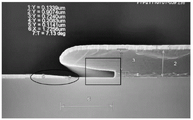
in the current Lift off process, as shown in fig. 2 and 3, the area 1 metal and the area 2 metal are sputtered metal at the same time, the area 1 metal will be stripped off in the future, and the area 2 metal is the metal to be retained and has a thickness of only 110 nm. Since this block of metal is used for special functions in the manufacture of filters for the block of metal in region 2, the block width of the metal in region 2 is an integer multiple of half the acoustic wavelength. The closer the zone 2 metal boundary angle is to 90 deg., the better. The middle LOR photoresist is a photoresist special for a Lift off process, and is used for specially manufacturing undercut (undercut) to prevent the metal in the region 2 from being completely attached to the photoresist for deposition, so that when the photoresist is cleaned by a subsequent Lift off process, the metal is attached to the photoresist region and torn, and the metal in the region 2 is pulled up. However, due to the retraction, it is likely that defects in the projected deposition will be caused, and the region 2 metal smearing effect will occur, the shorter this smearing is the better, i.e. the closer the side metal boundary angle is to 90 °, the better (the dotted circle in fig. 2). The traditional process has the problems that the LOR is correspondingly required to be thinner due to the thin metal thickness of the region 2, the process difficulty required by thinner LOR photoresist is increased, and the market price is increased by multiple times, for example, the price of the photoresist with the thickness of 300nm for the LOR is about 15000 RMB per liter, and the price of the photoresist with the thickness of 200nm for the LOR is 32000 RMB per liter. In addition to this price problem, there is a serious technical barrier, LOR is a wet etching process using an organic detergent to shrink it inward (circled part in the square of fig. 3), and the organic detergent slightly erodes the positive photoresist, which results in an obvious bell-mouth shape at the opening, thereby amplifying the side effect of the projected deposition, so that the metal deposition is smeared seriously, and the angle is often less than 10 ° (7.13 ° for circled part in fig. 3)
While the preferred embodiments and examples of the present invention have been described in detail, the present invention is not limited to the embodiments and examples, and various changes can be made without departing from the spirit of the present invention within the knowledge of those skilled in the art.