CN115242585A - Continuous time linear equalizer circuit based on feedforward technology - Google Patents
Continuous time linear equalizer circuit based on feedforward technology Download PDFInfo
- Publication number
- CN115242585A CN115242585A CN202211150974.9A CN202211150974A CN115242585A CN 115242585 A CN115242585 A CN 115242585A CN 202211150974 A CN202211150974 A CN 202211150974A CN 115242585 A CN115242585 A CN 115242585A
- Authority
- CN
- China
- Prior art keywords
- load
- signal
- frequency
- circuit
- mos transistor
- Prior art date
- Legal status (The legal status is an assumption and is not a legal conclusion. Google has not performed a legal analysis and makes no representation as to the accuracy of the status listed.)
- Granted
Links
- 238000005516 engineering process Methods 0.000 title abstract description 10
- 230000003321 amplification Effects 0.000 claims abstract description 10
- 238000003199 nucleic acid amplification method Methods 0.000 claims abstract description 10
- 230000005540 biological transmission Effects 0.000 claims abstract description 8
- 238000000034 method Methods 0.000 claims abstract description 8
- 239000003990 capacitor Substances 0.000 claims description 33
- 230000008878 coupling Effects 0.000 claims description 23
- 238000010168 coupling process Methods 0.000 claims description 23
- 238000005859 coupling reaction Methods 0.000 claims description 23
- 238000012546 transfer Methods 0.000 claims description 18
- 230000007850 degeneration Effects 0.000 claims description 15
- 230000015556 catabolic process Effects 0.000 claims description 11
- 238000006731 degradation reaction Methods 0.000 claims description 11
- 230000008054 signal transmission Effects 0.000 abstract description 4
- 238000013461 design Methods 0.000 abstract description 2
- 238000010586 diagram Methods 0.000 description 8
- 230000004044 response Effects 0.000 description 7
- 239000000203 mixture Substances 0.000 description 3
- 239000000284 extract Substances 0.000 description 1
- 238000012986 modification Methods 0.000 description 1
- 230000004048 modification Effects 0.000 description 1
- 230000008569 process Effects 0.000 description 1
- 238000012545 processing Methods 0.000 description 1
Images


Classifications
-
- H—ELECTRICITY
- H04—ELECTRIC COMMUNICATION TECHNIQUE
- H04L—TRANSMISSION OF DIGITAL INFORMATION, e.g. TELEGRAPHIC COMMUNICATION
- H04L25/00—Baseband systems
- H04L25/02—Details ; arrangements for supplying electrical power along data transmission lines
- H04L25/03—Shaping networks in transmitter or receiver, e.g. adaptive shaping networks
- H04L25/03006—Arrangements for removing intersymbol interference
- H04L25/03012—Arrangements for removing intersymbol interference operating in the time domain
- H04L25/03019—Arrangements for removing intersymbol interference operating in the time domain adaptive, i.e. capable of adjustment during data reception
- H04L25/03057—Arrangements for removing intersymbol interference operating in the time domain adaptive, i.e. capable of adjustment during data reception with a recursive structure
Landscapes
- Engineering & Computer Science (AREA)
- Power Engineering (AREA)
- Computer Networks & Wireless Communication (AREA)
- Signal Processing (AREA)
- Amplifiers (AREA)
Abstract
Description
技术领域technical field
本申请涉及电路设计技术领域,特别是涉及一种基于前馈技术的连续时间线性均衡器电路。The present application relates to the technical field of circuit design, and in particular, to a continuous-time linear equalizer circuit based on feedforward technology.
背景技术Background technique
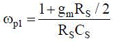
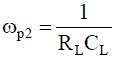
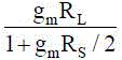
连续时间线性均衡(Continuous Time Linear Equalization,CTLE)通常用在高速串口的接收端,用于补偿非理想信道对高频分量的损耗。传统连续时间线性均衡采用源极退化形式的共源极放大器,电路结构如图1(a)所示,幅频响应如图1(b)所示,根据图1可以知道,传统连续时间线性均衡电路中包括输入信号Vip/Vin、输出信号Vout、电容CL、负载RL、源极退化电阻RS、退化电容CS和尾电流源,电路中的退化电阻RS和退化电容CS在传递函数中引入了一个零极点对(ωz,ωp1),从而在频率响应中引入了+20dB/dec的斜率,其中

发明内容SUMMARY OF THE INVENTION
基于此,有必要针对上述技术问题,提供一种能够保证信号传输质量,平衡高频补偿和低频增益的基于前馈技术的连续时间线性均衡器电路。Based on this, it is necessary to provide a continuous-time linear equalizer circuit based on feed-forward technology that can ensure the quality of signal transmission and balance high-frequency compensation and low-frequency gain in response to the above technical problems.
一种基于前馈技术的连续时间线性均衡器电路,所述电路包括:A continuous-time linear equalizer circuit based on feedforward technology, the circuit comprising:
输入端口,用于输入信道传输过程中的输入差分信号;Input port, used for input differential signal in the process of input channel transmission;
基本放大模块,用于对输入差分信号进行低频补偿,得到低频增益信号传输至输出端口;The basic amplifier module is used to perform low-frequency compensation on the input differential signal to obtain a low-frequency gain signal and transmit it to the output port;
前馈模块,用于根据高通选频网络提取输入差分信号中的高频信号进行高频补偿,得到高频增益信号传输至输出端口;The feedforward module is used to extract the high-frequency signal in the input differential signal according to the high-pass frequency selection network for high-frequency compensation, and obtain the high-frequency gain signal and transmit it to the output port;
输出端口,用于接收并叠加高频增益信号和低频增益信号,得到输出差分信号。The output port is used to receive and superimpose the high frequency gain signal and the low frequency gain signal to obtain the output differential signal.
在其中一个实施例中,基本放大模块包括第一MOS管、第三MOS管、第一负载、第二负载和第一尾电流源;In one of the embodiments, the basic amplifier module includes a first MOS transistor, a third MOS transistor, a first load, a second load and a first tail current source;
第一MOS管的栅极连接输入端口,根据输入端口输入所述输入差分信号中的第一输入信号,第三MOS管的栅极连接输入端口,根据输入端口输入所述输入差分信号中的第二输入信号,第一MOS管的漏极和第三MOS管的漏极通过第一负载和第二负载接入电源,第一MOS管的漏极连接输出端口输出所述输出差分信号中的第一输出信号,第三MOS管的漏极连接输出端口输出所述输出差分信号中的第二输出信号,第一MOS管的源极和第三MOS管的源极耦合在一起通过第一尾电流源接地。The gate of the first MOS transistor is connected to the input port, the first input signal of the input differential signals is input according to the input port, the gate of the third MOS transistor is connected to the input port, and the first input signal of the input differential signals is input according to the input port. Two input signals, the drain of the first MOS transistor and the drain of the third MOS transistor are connected to the power supply through the first load and the second load, and the drain of the first MOS transistor is connected to the output port to output the third output differential signal. An output signal, the drain of the third MOS transistor is connected to the output port to output the second output signal in the output differential signal, the source of the first MOS transistor and the source of the third MOS transistor are coupled together through the first tail current source to ground.
在其中一个实施例中,前馈模块包括第二MOS管、第四MOS管、耦合电容、前馈负载和第二尾电流源;In one of the embodiments, the feedforward module includes a second MOS transistor, a fourth MOS transistor, a coupling capacitor, a feedforward load and a second tail current source;
第二MOS管的漏极和第四MOS管的漏极通过前馈负载接入电源,第二MOS管的源极和第四MOS管的源极耦合在一起通过第二尾电流源接地,耦合电容的两端分别跨接在前馈负载的第二端和第一负载的第二端之间。The drain of the second MOS transistor and the drain of the fourth MOS transistor are connected to the power supply through the feedforward load, and the source of the second MOS transistor and the source of the fourth MOS transistor are coupled together to ground through the second tail current source, and the coupling Two ends of the capacitor are respectively connected between the second end of the feedforward load and the second end of the first load.
在其中一个实施例中,高通选频网络包括第一负载、前馈负载和耦合电容;In one of the embodiments, the high-pass frequency selective network includes a first load, a feedforward load and a coupling capacitor;
第一负载的第一端和前馈负载的第一端连接电源,第一负载的第二端与第二负载的第一端相连,前馈负载的第二端与第二MOS管的漏极或第四MOS管的漏极相连,耦合电容的两端分别跨接在前馈负载的第二端和第一负载的第二端之间。The first end of the first load and the first end of the feedforward load are connected to the power supply, the second end of the first load is connected to the first end of the second load, and the second end of the feedforward load is connected to the drain of the second MOS transistor Or the drain of the fourth MOS transistor is connected, and the two ends of the coupling capacitor are respectively connected between the second end of the feedforward load and the second end of the first load.
在其中一个实施例中,电路产生的第一电路传递函数为In one of the embodiments, the first circuit transfer function generated by the circuit is

其中,RL1表示第一负载,RL2表示第二负载,Cf表示耦合电容,Rf表示前馈负载,gm1表示第一MOS管或第三MOS管的跨导,gm2表示第二MOS管或第四MOS管的跨导,s表示频域。Among them, R L1 represents the first load, R L2 represents the second load, C f represents the coupling capacitor, R f represents the feedforward load, g m1 represents the transconductance of the first MOS transistor or the third MOS transistor, and g m2 represents the second The transconductance of the MOS transistor or the fourth MOS transistor, s represents the frequency domain.
在其中一个实施例中,第一电路传递函数产生的低频增益由基本放大模块确定,低频增益为
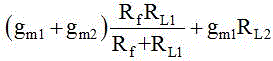
在其中一个实施例中,第一负载和前馈负载包括电阻或二极管形式的MOS管。In one of the embodiments, the first load and the feedforward load include MOS transistors in the form of resistors or diodes.
在其中一个实施例中,基本放大模块的组成形式还包括第一MOS管、第三MOS管、第一负载、第二负载、第一尾电流源以及退化电阻和退化电容,退化电阻和退化电容的两端分别跨接在第一MOS管的源极和第三MOS管的源极之间,退化电阻和退化电容并联,第一MOS管的源极和第三MOS管的源极分别通过第一尾电流源接地;In one of the embodiments, the composition form of the basic amplifier module further includes a first MOS transistor, a third MOS transistor, a first load, a second load, a first tail current source, a degeneration resistor and a degeneration capacitor, and a degeneration resistor and a degeneration capacitor. The two ends are respectively connected between the source of the first MOS tube and the source of the third MOS tube, the degradation resistance and the degradation capacitor are connected in parallel, and the source of the first MOS tube and the source of the third MOS tube pass through the A current source is grounded;
前馈模块的组成形式还包括第二MOS管、第四MOS管、耦合电容、前馈负载和第二尾电流源;The composition form of the feedforward module further includes a second MOS transistor, a fourth MOS transistor, a coupling capacitor, a feedforward load and a second tail current source;
高通选频网络的组成形式还包括第一负载、前馈负载和耦合电容。The composition form of the high-pass frequency selection network further includes a first load, a feedforward load and a coupling capacitor.
在其中一个实施例中,电路产生的第二电路传递函数为In one of the embodiments, the second circuit transfer function generated by the circuit is

其中,RL1表示所述第一负载,RL2表示所述第二负载,Cf表示所述耦合电容,Rf表示所述前馈负载,gm1表示第一MOS管或第三MOS管的跨导,gm2表示第二MOS管或第四MOS管的跨导,s表示频域,RS表示退化电阻,CS表示退化电容。Among them, R L1 represents the first load, R L2 represents the second load, C f represents the coupling capacitor, R f represents the feedforward load, and g m1 represents the first MOS transistor or the third MOS transistor. Transconductance, g m2 represents the transconductance of the second MOS transistor or the fourth MOS transistor, s represents the frequency domain, R S represents the degradation resistance, and C S represents the degradation capacitance.
在其中一个实施例中,第二电路传递函数产生的低频增益由基本放大模块确定,低频增益为
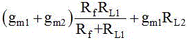
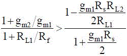
上述基于前馈技术的连续时间线性均衡器电路,通过输入端口将信道传输过程中的差分信号输入连续时间均衡器进行均衡处理,电路中的基本放大模块对输入差分信号进行低频补偿,得到低频增益信号,电路中的前馈模块根据高通选频网络提取输入差分信号中的高频分量并进行放大,得到高频增益信号,最后通过输出端口接收并叠加高频增益信号和低频增益信号,得到输出差分信号。采用本电路中的高通选频网络,可以将信道传输过程中受到损耗的输入差分信号中的高频信号提取至前馈模块进行高频补偿,使得低频增益与高频补偿之间相互独立,互不影响,有效避免了传统结构中高频补偿强度与低频增益相互制约的问题,从而保证了信号传输的质量。The above-mentioned continuous-time linear equalizer circuit based on feedforward technology inputs the differential signal in the channel transmission process into the continuous-time equalizer for equalization processing through the input port, and the basic amplification module in the circuit performs low-frequency compensation on the input differential signal to obtain low-frequency gain. signal, the feedforward module in the circuit extracts the high-frequency component in the input differential signal according to the high-pass frequency selection network and amplifies it to obtain the high-frequency gain signal, and finally receives and superimposes the high-frequency gain signal and the low-frequency gain signal through the output port to obtain the output. differential signal. Using the high-pass frequency selection network in this circuit, the high-frequency signal in the input differential signal that is lost during the channel transmission process can be extracted to the feedforward module for high-frequency compensation, so that the low-frequency gain and the high-frequency compensation are independent of each other. It does not affect, and effectively avoids the problem of mutual restriction between high-frequency compensation strength and low-frequency gain in the traditional structure, thereby ensuring the quality of signal transmission.
附图说明Description of drawings
图1为传统连续时间线性均衡图:图1(a)为电路结构示意图,图1(b)为幅频响应示意图;Figure 1 is a traditional continuous-time linear equalization diagram: Figure 1(a) is a schematic diagram of the circuit structure, and Figure 1(b) is a schematic diagram of the amplitude-frequency response;
图2为一个实施例中基于前馈技术的连续时间线性均衡器电路示意图;2 is a schematic diagram of a continuous-time linear equalizer circuit based on a feedforward technique in one embodiment;
图3为一个实施例中基于前馈技术的连续时间线性均衡器电路的幅频响应示意图;3 is a schematic diagram of an amplitude-frequency response of a continuous-time linear equalizer circuit based on a feedforward technique in one embodiment;
图4为一个实施例中负载为二极管形式的MOS管时的电路结构示意图:图4(a) 表示前馈负载为二极管形式的MOS管,图4(b)表示第一负载为二极管形式的MOS管;FIG. 4 is a schematic diagram of the circuit structure when the load is a diode-type MOS tube in one embodiment: FIG. 4(a) shows a MOS tube with a diode-shaped feedforward load, and FIG. 4(b) shows a diode-shaped MOS tube as the first load Tube;
图5为另一个实施例中基于前馈技术的连续时间线性均衡器电路示意图。FIG. 5 is a schematic diagram of a continuous-time linear equalizer circuit based on a feedforward technique in another embodiment.
具体实施方式Detailed ways
为了使本申请的目的、技术方案及优点更加清楚明白,以下结合附图及实施例,对本申请进行进一步详细说明。应当理解,此处描述的具体实施例仅仅用以解释本申请,并不用于限定本申请。In order to make the purpose, technical solutions and advantages of the present application more clearly understood, the present application will be described in further detail below with reference to the accompanying drawings and embodiments. It should be understood that the specific embodiments described herein are only used to explain the present application, but not to limit the present application.
需要说明,在本发明中如涉及“第一”、“第二”等的描述仅用于描述目的,而不能理解为指示或暗示其相对重要性或者隐含指明所指示的技术特征的数量。由此,限定有“第一”、“第二”的特征可以明示或者隐含地包括至少一个该特征。在本发明的描述中,“多个”的含义是至少两个,例如两个,三个等,除非另有明确具体的限定。It should be noted that descriptions such as "first", "second", etc. in the present invention are only for description purposes, and should not be interpreted as indicating or implying their relative importance or implicitly indicating the number of indicated technical features. Thus, a feature delimited with "first", "second" may expressly or implicitly include at least one of that feature. In the description of the present invention, "plurality" means at least two, such as two, three, etc., unless otherwise expressly and specifically defined.
在一个实施例中,提供了一种基于前馈技术的连续时间线性均衡器电路,电路结构如图2所示,包括:In one embodiment, a continuous-time linear equalizer circuit based on feedforward technology is provided, and the circuit structure is shown in FIG. 2 , including:
输入端口,用于输入信道传输过程中的输入差分信号Vip/Vin。The input port is used to input the input differential signal Vip/Vin during channel transmission.
基本放大模块,用于对所述输入差分信号进行低频补偿,得到低频增益信号传输至输出端口。其中,基本放大模块包括第一MOS管M1、第三MOS管M3、第一负载RL1、第二负载RL2和第一尾电流源I1;第一MOS管M1的栅极连接输入端口,根据输入端口输入所述输入差分信号中的第一输入信号Vip,第三MOS管M3的栅极连接输入端口,根据输入端口输入所述输入差分信号中的第二输入信号Vin,第一MOS管M1的漏极和第三MOS管M3的漏极通过第一负载RL1和第二负载RL2接入电源,第一MOS管M1的漏极连接输出端口输出所述输出差分信号中的第一输出信号Von,第三MOS管M3的漏极连接输出端口输出所述输出差分信号中的第二输出信号Vop,第一MOS管M1的源极和第三MOS管M3的源极耦合在一起通过第一尾电流源I1接地。The basic amplifying module is used to perform low-frequency compensation on the input differential signal to obtain a low-frequency gain signal and transmit it to the output port. The basic amplifier module includes a first MOS transistor M1, a third MOS transistor M3, a first load R L1 , a second load R L2 and a first tail current source I 1 ; the gate of the first MOS transistor M1 is connected to the input port, The first input signal Vip in the input differential signal is input according to the input port, the gate of the third MOS transistor M3 is connected to the input port, and the second input signal Vin in the input differential signal is input according to the input port, the first MOS transistor M3 The drain of M1 and the drain of the third MOS transistor M3 are connected to the power supply through the first load R L1 and the second load R L2 , and the drain of the first MOS transistor M1 is connected to the output port to output the first of the output differential signals The output signal Von, the drain of the third MOS transistor M3 is connected to the output port to output the second output signal Vop in the output differential signal, the source of the first MOS transistor M1 and the source of the third MOS transistor M3 are coupled together through The first tail current source I 1 is grounded.
前馈模块,用于根据高通选频网络提取所述输入差分信号中的高频信号进行高频补偿,得到高频增益信号传输至输出端口。其中,前馈模块包括第二MOS管M2、第四MOS管M4、耦合电容Cf、前馈负载Rf和第二尾电流源I2;第二MOS管M2的漏极和第四MOS管M4的漏极通过前馈负载Rf接入电源,第二MOSM2管的源极和第四MOS管M4的源极耦合在一起通过第二尾电流源I2接地,耦合电容Cf的两端分别跨接在前馈负载Rf的第二端和第一负载RL1的第二端之间。The feedforward module is used for extracting the high-frequency signal in the input differential signal according to the high-pass frequency selection network to perform high-frequency compensation, so as to obtain the high-frequency gain signal and transmit it to the output port. The feedforward module includes a second MOS transistor M2, a fourth MOS transistor M4, a coupling capacitor C f , a feedforward load R f and a second tail current source I 2 ; the drain of the second MOS transistor M2 and the fourth MOS transistor The drain of M4 is connected to the power supply through the feedforward load Rf , the source of the second MOSM2 transistor and the source of the fourth MOS transistor M4 are coupled together to ground through the second tail current source I2 , and both ends of the coupling capacitor Cf They are respectively connected between the second end of the feedforward load R f and the second end of the first load R L1 .
具体地,高通选频网络包括第一负载RL1、前馈负载Rf和耦合电容Cf;第一负载RL1的第一端和前馈负载Rf的第一端连接电源,第一负载RL1的第二端与第二负载RL2的第一端相连,前馈负载Rf的第二端与第二MOS管M2的漏极或第四MOS管M4的漏极相连,耦合电容Cf的两端分别跨接在前馈负载Rf的第二端和第一负载RL1的第二端之间。Specifically, the high-pass frequency selection network includes a first load R L1 , a feed-forward load R f and a coupling capacitor C f ; the first end of the first load R L1 and the first end of the feed-forward load R f are connected to the power supply, and the first load The second end of R L1 is connected to the first end of the second load R L2 , the second end of the feedforward load R f is connected to the drain of the second MOS transistor M2 or the drain of the fourth MOS transistor M4, and the coupling capacitor C Both ends of f are respectively connected between the second end of the feedforward load R f and the second end of the first load R L1 .
输出端口,用于接收并叠加所述高频增益信号和所述低频增益信号,得到输出差分信号Vop/Von。The output port is used for receiving and superimposing the high frequency gain signal and the low frequency gain signal to obtain the output differential signal Vop/Von.
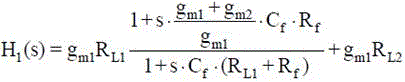
在本实施例中,通过上述基于前馈技术的连续时间线性均衡器电路产生的第一电路传递函数为In this embodiment, the first circuit transfer function generated by the above-mentioned continuous-time linear equalizer circuit based on the feedforward technology is:

式中,gm1表示第一MOS管或第三MOS管的跨导,gm2表示第二MOS管或第四MOS管的跨导,s表示频域。In the formula, g m1 represents the transconductance of the first MOS transistor or the third MOS transistor, g m2 represents the transconductance of the second MOS transistor or the fourth MOS transistor, and s represents the frequency domain.
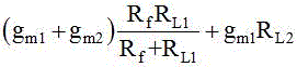
第一电路传递函数对应的幅频响应曲线如图3所示,由图3可知,前馈模块使得第一电路传递函数中产生了一对零极点(ωz,ωp),从而在幅频响应中引入了+20dB/dec的斜率,实现了高频补偿,其中,零点ωz处的低频增益由基本放大模块确定,不受前馈模块影响,低频增益为
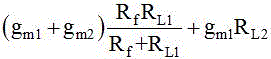
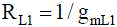
在其中一个实施例中,如图4所示,本发明所提的基于前馈技术的连续时间线性均衡器电路中的第一负载RL1和前馈负载Rf可以采用电阻形式,也可以采用连接成二极管形式的MOS管代替,由连接成二极管形式的MOS管组成的前馈负载Rf如图4(a)所示,其中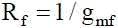
在另一个实施例中,本发明所提的基于前馈技术的连续时间线性均衡器电路可以由将前馈模块与图1中的传统连续时间线性均衡电路进行叠加得到,电路结构如图5所示,包括:In another embodiment, the continuous-time linear equalizer circuit based on the feed-forward technology proposed by the present invention can be obtained by superimposing the feed-forward module and the traditional continuous-time linear equalization circuit in FIG. 1 , and the circuit structure is shown in FIG. 5 . display, including:
输入端口,用于输入信道传输过程中的输入差分信号Vip/Vin。The input port is used to input the input differential signal Vip/Vin during channel transmission.
基本放大模块,用于对所述输入差分信号进行低频补偿,得到低频增益信号传输至输出端口。其中,基本放大模块包括第一MOS管M1、第三MOS管M3、第一负载RL1、第二负载RL2、第一尾电流源I1、退化电阻Rs与退化电容Cs;第一MOS管M1的栅极连接输入端口,根据输入端口输入所述输入差分信号中的第一输入信号Vip,第三MOS管M3的栅极连接输入端口,根据输入端口输入所述输入差分信号中的第二输入信号Vin,第一MOS管M1的漏极和第三MOS管M3的漏极通过第一负载RL1和第二负载RL2接入电源,第一MOS管M1的漏极连接输出端口输出所述输出差分信号中的第一输出信号Von,第三MOS管M3的漏极连接输出端口输出所述输出差分信号中的第二输出信号Vop,退化电阻RS和退化电容CS的两端分别跨接在第一MOS管M1的源极和第三MOS管M3的源极之间,退化电阻RS和退化电容CS并联,第一MOS管M1的源极和第三MOS管M3的源极分别通过第一尾电流源I1接地。The basic amplifying module is used to perform low-frequency compensation on the input differential signal to obtain a low-frequency gain signal and transmit it to the output port. The basic amplifier module includes a first MOS transistor M1, a third MOS transistor M3, a first load R L1 , a second load R L2 , a first tail current source I 1 , a degradation resistor Rs and a degradation capacitor Cs; the first MOS tube The gate of M1 is connected to the input port, the first input signal Vip of the input differential signals is input according to the input port, the gate of the third MOS transistor M3 is connected to the input port, and the second input differential signal is input according to the input port. Inputting the signal Vin, the drain of the first MOS transistor M1 and the drain of the third MOS transistor M3 are connected to the power supply through the first load R L1 and the second load R L2 , and the drain of the first MOS transistor M1 is connected to the output port of the output port. The first output signal Von in the output differential signal, the drain of the third MOS transistor M3 is connected to the output port to output the second output signal Vop in the output differential signal, the two ends of the degradation resistor R S and the degradation capacitor C S are respectively Connected across the source of the first MOS transistor M1 and the source of the third MOS transistor M3, the degradation resistor R S and the degradation capacitor C S are connected in parallel, the source of the first MOS transistor M1 and the source of the third MOS transistor M3 The poles are respectively grounded through the first tail current source I1 .
前馈模块,用于根据高通选频网络提取所述输入差分信号中的高频信号进行高频补偿,得到高频增益信号传输至输出端口。其中,前馈模块包括第二MOS管M2、第四MOS管M4、耦合电容Cf、前馈负载Rf和第二尾电流源I2;第二MOS管M2的漏极和第四MOS管M4的漏极通过前馈负载Rf接入电源,第二MOS管M2的源极和第四MOS管M4的源极耦合在一起通过第二尾电流源I2接地,耦合电容Cf的两端分别跨接在前馈模块上的前馈负载Rf的第二端和基本放大模块上的第一负载RL1的第二端之间。The feedforward module is used for extracting the high-frequency signal in the input differential signal according to the high-pass frequency selection network to perform high-frequency compensation, so as to obtain the high-frequency gain signal and transmit it to the output port. The feedforward module includes a second MOS transistor M2, a fourth MOS transistor M4, a coupling capacitor C f , a feedforward load R f and a second tail current source I 2 ; the drain of the second MOS transistor M2 and the fourth MOS transistor The drain of M4 is connected to the power supply through the feedforward load Rf , the source of the second MOS transistor M2 and the source of the fourth MOS transistor M4 are coupled together to ground through the second tail current source I2 , and the two coupling capacitors Cf The terminals are respectively connected between the second terminal of the feed-forward load R f on the feed-forward module and the second terminal of the first load R L1 on the basic amplifying module.
具体地,高通选频网络包括第一负载RL1、前馈负载Rf和耦合电容Cf;基本放大模块上的第一负载RL1的第一端连接电源,第一负载RL1的第二端与第二负载RL2的第一端相连,前馈模块上的前馈负载Rf的第一端连接电源,前馈负载Rf的第二端与第二MOS管M2的漏极或第四MOS管M4的漏极相连,耦合电容Cf的两端分别跨接在在前馈模块上的前馈负载Rf的第二端和基本放大模块上的第一负载RL1的第二端之间。Specifically, the high-pass frequency selection network includes a first load R L1 , a feed-forward load R f and a coupling capacitor C f ; the first end of the first load R L1 on the basic amplifier module is connected to the power supply, and the second end of the first load R L1 is connected to the power supply. The terminal is connected to the first terminal of the second load R L2 , the first terminal of the feed-forward load R f on the feed-forward module is connected to the power supply, and the second terminal of the feed-forward load R f is connected to the drain or the first terminal of the second MOS transistor M2. The drains of the four MOS transistors M4 are connected, and the two ends of the coupling capacitor C f are respectively connected across the second end of the feedforward load R f on the feedforward module and the second end of the first load R L1 on the basic amplifier module between.
输出端口,用于接收并叠加所述高频增益信号和所述低频增益信号,得到输出差分信号Vop/Von。The output port is used for receiving and superimposing the high frequency gain signal and the low frequency gain signal to obtain the output differential signal Vop/Von.
在本实施例中,通过上述基于前馈技术的连续时间线性均衡器电路产生的第二电路传递函数为In this embodiment, the second circuit transfer function generated by the above-mentioned continuous-time linear equalizer circuit based on the feedforward technique is:

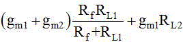
可以发现,第二电路传递函数的低频增益由基本放大模块确定,低频增益为低频增益为
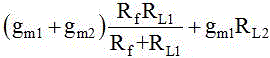
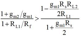
以上实施例的各技术特征可以进行任意的组合,为使描述简洁,未对上述实施例中的各个技术特征所有可能的组合都进行描述,然而,只要这些技术特征的组合不存在矛盾,都应当认为是本说明书记载的范围。The technical features of the above embodiments can be combined arbitrarily. In order to make the description simple, all possible combinations of the technical features in the above embodiments are not described. However, as long as there is no contradiction in the combination of these technical features It is considered to be the range described in this specification.
以上所述实施例仅表达了本申请的几种实施方式,其描述较为具体和详细,但并不能因此而理解为对发明专利范围的限制。应当指出的是,对于本领域的普通技术人员来说,在不脱离本申请构思的前提下,还可以做出若干变形和改进,这些都属于本申请的保护范围。因此,本申请专利的保护范围应以所附权利要求为准。The above-mentioned embodiments only represent several embodiments of the present application, and the descriptions thereof are specific and detailed, but should not be construed as a limitation on the scope of the invention patent. It should be pointed out that for those skilled in the art, without departing from the concept of the present application, several modifications and improvements can be made, which all belong to the protection scope of the present application. Therefore, the scope of protection of the patent of the present application shall be subject to the appended claims.
Claims (9)



Priority Applications (1)
| Application Number | Priority Date | Filing Date | Title |
|---|---|---|---|
| CN202211150974.9A CN115242585B (en) | 2022-09-21 | 2022-09-21 | Continuous Time Linear Equalizer Circuit Based on Feedforward Technology |
Applications Claiming Priority (1)
| Application Number | Priority Date | Filing Date | Title |
|---|---|---|---|
| CN202211150974.9A CN115242585B (en) | 2022-09-21 | 2022-09-21 | Continuous Time Linear Equalizer Circuit Based on Feedforward Technology |
Publications (2)
| Publication Number | Publication Date |
|---|---|
| CN115242585A true CN115242585A (en) | 2022-10-25 |
| CN115242585B CN115242585B (en) | 2022-12-09 |
Family
ID=83681714
Family Applications (1)
| Application Number | Title | Priority Date | Filing Date |
|---|---|---|---|
| CN202211150974.9A Active CN115242585B (en) | 2022-09-21 | 2022-09-21 | Continuous Time Linear Equalizer Circuit Based on Feedforward Technology |
Country Status (1)
| Country | Link |
|---|---|
| CN (1) | CN115242585B (en) |
Cited By (2)
| Publication number | Priority date | Publication date | Assignee | Title |
|---|---|---|---|---|
| CN115514598A (en) * | 2022-10-28 | 2022-12-23 | 中国人民解放军国防科技大学 | Continuous Time Linear Equalization Circuit Based on Inverter Negative Capacitance Compensation |
| CN117439596A (en) * | 2023-08-09 | 2024-01-23 | 慷智集成电路(上海)有限公司 | A receiving circuit, deserializing circuit chip, electronic equipment and vehicle |
Citations (9)
| Publication number | Priority date | Publication date | Assignee | Title |
|---|---|---|---|---|
| CN103746671A (en) * | 2014-01-24 | 2014-04-23 | 南京邮电大学 | Equalizing filter with high gain and wide compensation range |
| US9473330B1 (en) * | 2015-06-05 | 2016-10-18 | International Business Machines Corporation | Continuous time linear equalizer with a programmable negative feedback amplification loop |
| CN108353044A (en) * | 2015-10-28 | 2018-07-31 | 华为技术有限公司 | Combine low frequency and high frequency continuous time linear equalizer |
| US10263815B1 (en) * | 2017-12-11 | 2019-04-16 | Xilinx, Inc. | Continuous time linear equalization |
| US20190305810A1 (en) * | 2018-04-03 | 2019-10-03 | Semiconductor Components Industries, Llc | Methods and apparatus for a continuous time linear equalizer |
| CN113489465A (en) * | 2021-07-22 | 2021-10-08 | 苏州瀚宸科技有限公司 | Amplifier circuit |
| CN113691234A (en) * | 2020-05-18 | 2021-11-23 | 恩智浦有限公司 | High-bandwidth continuous time linear equalization circuit |
| US20220103400A1 (en) * | 2020-09-30 | 2022-03-31 | Mediatek Singapore Pte. Ltd | Low power receiver with equalization circuit, communication unit and method therefor |
| CN114301441A (en) * | 2021-12-31 | 2022-04-08 | 苏州芯动微电子科技有限公司 | Linear equalizer and MIPI C-PHY circuit |
-
2022
- 2022-09-21 CN CN202211150974.9A patent/CN115242585B/en active Active
Patent Citations (9)
| Publication number | Priority date | Publication date | Assignee | Title |
|---|---|---|---|---|
| CN103746671A (en) * | 2014-01-24 | 2014-04-23 | 南京邮电大学 | Equalizing filter with high gain and wide compensation range |
| US9473330B1 (en) * | 2015-06-05 | 2016-10-18 | International Business Machines Corporation | Continuous time linear equalizer with a programmable negative feedback amplification loop |
| CN108353044A (en) * | 2015-10-28 | 2018-07-31 | 华为技术有限公司 | Combine low frequency and high frequency continuous time linear equalizer |
| US10263815B1 (en) * | 2017-12-11 | 2019-04-16 | Xilinx, Inc. | Continuous time linear equalization |
| US20190305810A1 (en) * | 2018-04-03 | 2019-10-03 | Semiconductor Components Industries, Llc | Methods and apparatus for a continuous time linear equalizer |
| CN113691234A (en) * | 2020-05-18 | 2021-11-23 | 恩智浦有限公司 | High-bandwidth continuous time linear equalization circuit |
| US20220103400A1 (en) * | 2020-09-30 | 2022-03-31 | Mediatek Singapore Pte. Ltd | Low power receiver with equalization circuit, communication unit and method therefor |
| CN113489465A (en) * | 2021-07-22 | 2021-10-08 | 苏州瀚宸科技有限公司 | Amplifier circuit |
| CN114301441A (en) * | 2021-12-31 | 2022-04-08 | 苏州芯动微电子科技有限公司 | Linear equalizer and MIPI C-PHY circuit |
Cited By (2)
| Publication number | Priority date | Publication date | Assignee | Title |
|---|---|---|---|---|
| CN115514598A (en) * | 2022-10-28 | 2022-12-23 | 中国人民解放军国防科技大学 | Continuous Time Linear Equalization Circuit Based on Inverter Negative Capacitance Compensation |
| CN117439596A (en) * | 2023-08-09 | 2024-01-23 | 慷智集成电路(上海)有限公司 | A receiving circuit, deserializing circuit chip, electronic equipment and vehicle |
Also Published As
| Publication number | Publication date |
|---|---|
| CN115242585B (en) | 2022-12-09 |
Similar Documents
| Publication | Publication Date | Title |
|---|---|---|
| US7683720B1 (en) | Folded-cascode amplifier with adjustable continuous time equalizer | |
| US7636003B2 (en) | Limiting amplifiers | |
| US9473330B1 (en) | Continuous time linear equalizer with a programmable negative feedback amplification loop | |
| CN108353044B (en) | Combined low and high frequency continuous time linear equalizer | |
| CN101388651B (en) | Receiver for high-speed digital interface | |
| CN103346778B (en) | A kind of broadband linear equalization circuit | |
| CN115242585B (en) | Continuous Time Linear Equalizer Circuit Based on Feedforward Technology | |
| CN110268626B (en) | Bias Modulated Active Linearization of Broadband Amplifiers | |
| GB2415339A (en) | A negative impedance receiver equaliser | |
| JPH077345A (en) | Variable equalizing amplifier | |
| US8907729B2 (en) | Trans-impedance amplifier for high speed optical-electrical interfaces | |
| CN111464203A (en) | High-speed full-duplex transceiver | |
| CN113098440B (en) | De-emphasis continuous time linear equalizer architecture | |
| JP2019036839A (en) | Transimpedance amplifier | |
| CN101110576A (en) | limiting amplifier | |
| CN103379063A (en) | Linear equalizer | |
| CN116111980A (en) | A low-power receiver analog front-end equalization circuit based on gm-TIA | |
| US7696838B2 (en) | Equalizing filter circuit | |
| CN108390657B (en) | Active inductance-based broadband analog equalizer integrated circuit | |
| KR101209817B1 (en) | Parallel Equalizer | |
| CN218071446U (en) | Distributed amplifier circuit adopting current multiplexing structure and unidirectional technology | |
| CN114785365B (en) | Capacitor-assisted three-coil transformer circuit | |
| CN118117990A (en) | High bandwidth, easily adjustable continuous time linear equalizer | |
| US11177984B1 (en) | CMOS analog circuits having a triode-based active load | |
| Chen et al. | Design of 10 GHz CMOS Optoelectronic Receiver Analog Front-End in Low-Cost 0.18 µm CMOS Technology |
Legal Events
| Date | Code | Title | Description |
|---|---|---|---|
| PB01 | Publication | ||
| PB01 | Publication | ||
| SE01 | Entry into force of request for substantive examination | ||
| SE01 | Entry into force of request for substantive examination | ||
| GR01 | Patent grant | ||
| GR01 | Patent grant |