Delayed frequency modulation demodulation circuit
The present invention relates to frequency modulation demodulation circuit, particularly relate to delayed frequency modulation demodulation circuit, this circuit is used for for example two sound accompaniment broadcast receivers of EIAJ (Japanese Industrial Standards' meeting, promptly Japanese Electronic Industries Association) NTSC television system NTSC and home VTR playback apparatus (VTR) etc.
In frequency with respect to carrier signal, the FM signal that the frequency band occupation rate is big, for example the secondary acoustical signal of the two sound accompaniment broadcasting of EIAJ NTSC television system NTSC and the briliancy tracer signal of home VTR etc. are separated timing, generally use delayed frequency modulation demodulation circuit shown in Figure 10.
In the frequency modulation demodulation circuit of Figure 10, the 101st, limiting amplifier (amplitude amplifier), the 102nd, delay circuit, the 103rd, mlultiplying circuit, the 104th, LPF (low pass filter).
Figure 11 is illustrated in the delayed frequency modulation demodulation circuit of Figure 10, the each several part waveform example of the action when 1/4 time of input signal cycle equated with the time of delay of delay circuit.
Figure 12 is illustrated in the delayed frequency modulation demodulation circuit of Figure 10, the each several part waveform example of the action when incoming frequency is lower than frequency shown in Figure 11.
Figure 13 is illustrated in the delayed frequency modulation demodulation circuit of Figure 10, the each several part waveform example of the action when incoming frequency is higher than frequency shown in Figure 11.
Below to the operating principle of the fm demodulation in the delayed frequency modulation demodulation circuit of Figure 10, the situation of contained secondary acoustical signal (FM signal) (for example shown in Figure 14 (a)) input is an example in the received signal with the two sound accompaniments broadcasting of the TV of EIAJ system, is illustrated with reference to the oscillogram of Figure 11~Figure 13.
(S101) by being divided into two-way after amplifier 101 shapings that are limited, one road signal (S102) is directly imported mlultiplying circuit to the input signal of frequency modulation (FM signal), and another road signal is postponed certain hour by the 1st delay circuit 102.This inhibit signal (S103) is also imported described mlultiplying circuit 103, and mlultiplying circuit 103 multiplies each other two input signals, output multiplying output signal (S104).The work period of this multiplying output signal (S104) the cycle of input signal be in the scope more than 2 times of time of delay with the proportional variation of incoming frequency.
Existing delayed frequency modulation demodulation circuit, postpone aspect the principle of signal multiplication of certain hour at input signal with it, make in the multiplying output signal (S104), shown in Figure 14 (b), the twice that produces with frequency input signal is the high order harmonic component composition of first-harmonic.
Therefore, in case multiplying output signal (S104) is become smoothly, promptly obtain proportional signal voltage of work period (S105) with multiplying output signal (S104) by means of low pass filter 104.That is to say that the high order harmonic component by means of using 2 times of low pass filter 104 filtering frequency input signals can obtain the fm demodulation signal (secondary acoustical signal) that is directly proportional with frequency input signal.
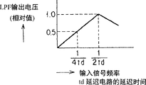
Again, be arbitrarily the time of delay of described delay circuit, and in input signal cycle was the scope below 2 times of time of delay, as shown in figure 15, the fm demodulation output voltage became and is not directly proportional with incoming frequency.Thereby, in order to carry out fm demodulation undistortedly, must design the time of delay of delay circuit than input signal the signal period during towards positive direction skew peak frequency 1/2 short.In time of delay is under 1/4 the situation of carrier cycle, and the scope that can carry out fm demodulation reaches maximum undistortedly, therefore, will be designed to 1/4 of carrier cycle time of delay usually.
But, as the secondary acoustical signal of the two sound accompaniment broadcast receivers of the TV of above-mentioned EIAJ system and the briliancy tracer signal of family expenses VTR playback apparatus, with respect to carrier frequency, under the big situation of frequency band occupation rate, the frequency of the frequency of restituted signal high frequency composition and high order harmonic component low frequency composition is close, thereby, for the filtering high order harmonic component, do not make the decay of restituted signal high frequency composition again, need to use the precipitous low pass filter of attenuation characteristic.
But, the precipitous common phase characteristic of low pass filter of attenuation characteristic changes greatly, thereby in the VTR signal processing circuit of handling picture signal and calculation process main audio signal and secondary acoustical signal, to the stereo two sound demodulation circuit that carry out demodulation, can not use the precipitous low pass filter of attenuation characteristic.Therefore, the actual low pass filter that uses 104 is according to setting its characteristic to the balance of attenuation characteristic and phase characteristic, and still, owing to can not fully guarantee attenuation characteristic, the output of low pass filter 104 has high order harmonic component to leak.
Figure 16 is that the secondary acoustical signal that the existing delayed frequency modulation demodulation circuit of expression is used for the two sound accompaniments broadcasting of TV of EIAJ system is separated the waveform of the high order harmonic component leakage situation of timing.At this moment condition is, be 1/4 of carrier cycle the time of delay of delay circuit, and input signal is 1KHz, do not have modulation, and at the mlultiplying circuit outlet side, No. 1 low pass filter and the cut-off frequency of cut-off frequency 15.734KHz are No. 1 the low pass filter cascade of 2.12KHz.The oscillogram leakage of high order harmonic component as can be seen from Figure 16.
Figure 17 and Figure 18 represent that existing delayed frequency modulation demodulation circuit is used for the waveform and the frequency spectrum of demodulation output under the situation of secondary acoustical signal demodulation of the two sound accompaniments broadcasting of TV of EIAJ system.At this moment condition is, be 1/4 of carrier cycle the time of delay of delay circuit, and input signal is 1KHz, and modulation degree is 100%, and at the mlultiplying circuit output, No. 1 low pass filter and the cut-off frequency of cut-off frequency 15.734KHz are No. 1 the low pass filter cascade of 2.12KHz.Be easy to find out the leakage of high order harmonic component from Figure 17 and Figure 18.
As mentioned above, existing delayed frequency modulation demodulation circuit for the filtering high order harmonic component, does not make the contained restituted signal high-frequency composition decay of multiplying output signal again, needs the precipitous low pass filter of attenuation characteristic.But, the actual low pass filter that uses, its characteristic is set according to the balance to attenuation characteristic and phase characteristic, and the attenuation characteristic of low pass filter can not fully be guaranteed, thereby the problem that exists low pass filter to have high order harmonic component to leak.
The present invention carries out for addressing the above problem, it is higher frequency that purpose is to provide the frequency translation of the high order harmonic component that can make the restituted signal that the computing output signal comprised, even have the delayed frequency modulation demodulation circuit that also can remove high order harmonic component under the situation of low pass filter of milder attenuation characteristic in use.
Delayed frequency modulation demodulation circuit of the present invention is characterised in that to possess: the 1st kind of means of the 1st signal that obtain the 1/2 short random time of the signal period of from retardation ratio fm input signal to positive direction skew peak frequency, in 1/2 time of lacking, obtain the 2nd kind of means of the 2nd signal of the random time longer than the time of delay of above-mentioned the 1st signal of input signal retardation ratio than the signal period of above-mentioned input signal when positive direction is offset peak frequency, in 1/2 time of lacking, obtain the 3rd kind of means of the 3rd signal of the random time longer than the time of delay of above-mentioned the 2nd signal of input signal retardation ratio than the signal period of above-mentioned input signal when positive direction is offset peak frequency, the 1st mlultiplying circuit with above-mentioned input signal and above-mentioned the 1st signal multiplication, the 2nd mlultiplying circuit with above-mentioned the 2nd signal and above-mentioned the 3rd signal multiplication, and with the add circuit of the output signal addition of the output signal of above-mentioned the 1st mlultiplying circuit and the 2nd mlultiplying circuit.
Fig. 1 is the block diagram of the delayed frequency modulation demodulation circuit of expression the present invention the 1st embodiment.
Fig. 2 is the waveform example of the each several part that shows for the action of the delayed frequency modulation demodulation circuit of presentation graphs 1.
Fig. 3 is the waveform example of the each several part that shows for the action of frequency input signal in the delayed frequency modulation demodulation circuit of presentation graphs 1 when lower than frequency shown in Figure 2.
Fig. 4 is the waveform example of the each several part that shows for the action of frequency input signal in the delayed frequency modulation demodulation circuit of presentation graphs 1 when higher than frequency shown in Figure 2.
Fig. 5 is an example of the delayed frequency modulation demodulation circuit of presentation graphs 1 frequency band range of input signal and output signal when the secondary acoustical signal input that is comprised in the two sound accompaniment broadcast singals of TV of EIAJ system is arranged.
Fig. 6 is the oscillogram that secondary acoustical signal that the delayed frequency modulation demodulation circuit of presentation graphs 1 is used for the two sound accompaniments broadcasting of TV of EIAJ system is separated the situation that the timing high order harmonic component leaks.
Fig. 7 is the oscillogram that secondary acoustical signal that the delayed frequency modulation demodulation circuit of presentation graphs 1 is used for the two sound accompaniments broadcasting of TV of EIAJ system is separated the demodulation output of timing.
Fig. 8 is that the secondary acoustical signal that the delayed frequency modulation demodulation circuit of presentation graphs 1 is used for the two sound accompaniments broadcasting of TV of EIAJ system is separated the frequency spectrum of the demodulation output of timing.
Fig. 9 is the block diagram of the delayed frequency modulation demodulation circuit of expression the present invention the 2nd embodiment.
Figure 10 is the block diagram of existing delayed frequency modulation demodulation circuit.
Figure 11 is the waveform example of the each several part that shows for the action of representing existing delayed frequency modulation demodulation circuit.
The waveform example of the each several part that the action of Figure 12 when representing that incoming frequency is lower than frequency shown in Figure 11 in the existing delayed frequency modulation demodulation circuit shown.
The waveform example of the each several part that the action of Figure 13 when representing that incoming frequency is higher than frequency shown in Figure 11 in the existing delayed frequency modulation demodulation circuit shown.
An example of the frequency band range of input signal and output signal when Figure 14 represents that the secondary acoustical signal that is comprised in the two sound accompaniment broadcast singals of the TV of EIAJ system is imported existing delayed frequency modulation demodulation circuit.
Figure 15 is the performance plot of the relation of frequency input signal and fm demodulation output voltage in the existing delayed frequency modulation demodulation circuit of expression.
Figure 16 is the oscillogram that secondary acoustical signal that the existing delayed frequency modulation demodulation circuit of expression is used for the two sound accompaniments broadcasting of TV of EIAJ system is separated the situation that the timing high order harmonic component leaks.
Figure 17 is the oscillogram of demodulation output under the situation of secondary acoustical signal demodulation of the existing delayed frequency modulation demodulation circuit of the expression two sound accompaniments broadcasting of TV that are used for the EIAJ system.
Figure 18 is the frequency spectrum that secondary acoustical signal that the existing delayed frequency modulation demodulation circuit of expression is used for the two sound accompaniments broadcasting of TV of EIAJ system is separated the frequency modulation output frequency of timing.
With reference to the accompanying drawings embodiments of the invention are elaborated.
Fig. 1 represents the delayed frequency modulation demodulation circuit of the present invention the 1st embodiment.In the delayed frequency modulation demodulation circuit of Fig. 1, the 11st, the signal (S11) through fm demodulation is carried out the amplitude limiting amplifier circuit that amplitude limit amplifies.
The 12nd, make the output signal (S12) of above-mentioned amplitude limiting amplifier circuit postpone certain hour, obtain the 1st delay circuit of the 1st inhibit signal (S13).The 13rd, make the output signal (S13) of above-mentioned the 1st delay circuit postpone certain hour, obtain the 2nd delay circuit of the 2nd inhibit signal (S14).The 14th, make the output signal (S14) of above-mentioned the 2nd delay circuit postpone certain hour, obtain the 3rd delay circuit of the 3rd inhibit signal (S15).
The 15th, the 1st mlultiplying circuit that the output signal (S12) and above-mentioned the 1st inhibit signal (S13) of above-mentioned amplitude limiting amplifier circuit multiplied each other, the 16th, the 2nd mlultiplying circuit that described the 2nd inhibit signal (S14) and described the 3rd inhibit signal (S15) are multiplied each other, the 17th, with the add circuit of output signal (S17) addition of the output signal (S16) of above-mentioned the 1st mlultiplying circuit 15 and the 2nd mlultiplying circuit 16.
The 18th, be used to import the output signal (S18) of above-mentioned add circuit 17, the low pass filter of the spuious high order harmonic component of filtering.
That is to say, in the delayed frequency modulation demodulation circuit of Fig. 1, it is (as described below to generate the time that postpones to become big in regular turn than input signal in 1/2 of the signal period during to positive direction skew peak frequency than fm input signal short random time, preferably 1/8 of carrier cycle, 1/4,3/8) the 1st~the 3rd signal, with the 1st mlultiplying circuit 15 with input signal and the 1st signal multiplication, with the 2nd mlultiplying circuit 16 with the 2nd signal and and the 3rd signal multiplication, with add circuit 17 with the output signal of the 1st mlultiplying circuit and the output signal addition of the 2nd mlultiplying circuit.
Fig. 2 is the waveform example of the each several part that shows for the action of the delayed frequency modulation demodulation circuit of presentation graphs 1.
Fig. 3 is the waveform example of the each several part that shows for the action of frequency input signal in the delayed frequency modulation demodulation circuit of presentation graphs 1 when lower than frequency shown in Figure 2.
Fig. 4 is the waveform example of the each several part that shows for the action of frequency input signal in the delayed frequency modulation demodulation circuit of presentation graphs 1 when higher than frequency shown in Figure 2.
Below to the operating principle of the fm demodulation of the delayed frequency modulation demodulation circuit of Fig. 1, with for example shown in Figure 2, the situation of contained secondary acoustical signal (FM signal) input is an example in the received signal of the two sound accompaniment broadcasting of EIAJ NTSC television system NTSC, is illustrated with reference to Fig. 2~oscillogram shown in Figure 4.
Frequency-modulatd FM signal input (S11) is undertaken being divided into two parts after the shaping by amplitude limiting amplifier circuit, and a part of signal (S12) is directly imported the 1st mlultiplying circuit 15, and another part is imported the 1st delay circuit 12.12 outputs of above-mentioned the 1st delay circuit have postponed the 1st inhibit signal (S13) of certain hour with input signal.The output signal of above-mentioned the 1st delay circuit 12 is divided into two parts, and a part of signal (S13) is directly imported following formula the 1st mlultiplying circuit 15, and another part signal is imported the 2nd delay circuit.13 outputs of above-mentioned the 2nd delay circuit postpone the 2nd inhibit signal (S14) of certain hour with input signal.The output signal of above-mentioned the 2nd delay circuit 13 is divided into two parts, and a part of signal (S14) is directly imported above-mentioned the 2nd mlultiplying circuit 16, and another part signal is imported the 3rd delay circuit 14.14 outputs of above-mentioned the 3rd delay circuit postpone the 3rd inhibit signal (S15) of certain hour with input signal, and it is imported above-mentioned the 2nd mlultiplying circuit 16.
Above-mentioned the 1st mlultiplying circuit 15 multiplies each other two input signals, obtains the 1st multiplication output signal (S16).And above-mentioned the 2nd mlultiplying circuit 16 multiplies each other two input signals, obtains the 2nd multiplication output signal (S17).
Utilize said method, make the frequency of work period of the 1st multiplication output signal (S16) and input signal proportional, the work period of the 2nd multiplication output signal (S17) is also proportional with the frequency of input signal.In this case, the 2nd multiplication output signal (S17) has postponed the time identical with the time of delay of the 2nd delay circuit 13 than the 1st multiplication output signal (S16).
And add circuit 17 obtains addition output signal (S18) with above-mentioned the 1st multiplication output signal (S16) and the 2nd multiplication output signal (S17) addition.Above-mentioned two signals (S16) (S17) as previously mentioned, have and proportional work period of the frequency of input signal, and therefore, addition output signal (S18) also has and proportional work period of the frequency of input signal.
Again, the 1st multiplication output signal (S16) and the 2nd multiplication output signal (S17) include 2 times high order harmonic component of input signal, and the 2nd multiplication output signal (S17), as mentioned above, postpone the time identical with the time of delay of the 2nd delay circuit 13 than the 1st multiplication output signal (S16).Therefore, the part of 2 times high order harmonic component of the output signal frequency that comprised of the 1st multiplication output signal (S16) and the 2nd multiplication output signal (S17) is transformed to four times high order harmonic component of frequency input signal.
Therefore, addition output signal (S18) in a single day becomes smoothly owing to the effect of low pass filter 18, can obtain the fm demodulation signal (secondary acoustical signal) that is directly proportional with the frequency of input signal.
As mentioned above, 2 times high order harmonic component of the frequency input signal of addition output signal (S18) institute conversion has reduced the share that is for conversion into the high order harmonic component that is four times in frequency input signal, therefore, when low pass filter uses the low pass filter with attenuation characteristic identical with the low pass filter of insertion mlultiplying circuit output in the existing delayed frequency modulation demodulation circuit, can make the leakage of high order harmonic component leak little than the high order harmonic component of existing delayed frequency modulation demodulation circuit.
Particularly, if be decided to be 1/8 of carrier cycle the time of delay of the 1st delay circuit the 12, the 2nd delay circuit 13 and the 3rd delay circuit 14 respectively, when frequency input signal equates with carrier frequency, the high order harmonic component that addition output signal (S18) is comprised has only four times high order harmonic component composition of frequency input signal, two times high order harmonic component composition is removed fully, and it is maximum that detection efficiency also reaches.
Fig. 6 is the waveform that secondary acoustical signal that the delayed frequency modulation demodulation circuit of presentation graphs 1 is used for the two sound accompaniments broadcasting of TV of EIAJ system is separated the situation that the high order harmonic component of timing leaks.At this moment condition is, be 1/8 of carrier cycle the time of delay of all delay circuits, input signal is modulation not, and cut-off frequency is that No. 1 low pass filter of 15.734KHz and 1 low-pass filter stage that cut-off frequency is 2.12KHz are coupled on the output of mlultiplying circuit.
From the waveform of Fig. 6 as can be seen, the leakage of high order harmonic component when using existing delayed frequency modulation demodulation circuit, high order harmonic component shown in Figure 16 leaks and will reduce about 22dB.
Fig. 7 represents that delayed frequency modulation demodulation circuit shown in Figure 1 is used for the demodulation output waveform that the secondary acoustical signal of the two sound accompaniments broadcasting of TV of EIAJ system is separated timing.At this moment condition is, be 1/8 of carrier cycle the time of delay of all delay circuits, input signal 1KHz, modulation degree is 100%, and cut-off frequency is that No. 1 low pass filter of 15.734KHz and 1 low-pass filter stage that cut-off frequency is 2.12KHz are coupled on the output of mlultiplying circuit.
As can be seen from Figure 7, the characteristic shown in Figure 17 during with the existing delayed frequency modulation demodulation circuit of use is compared, and the high order harmonic component that leaks into demodulation output has reduced.
Fig. 8 represents the frequency spectrum of frequency modulation output shown in Figure 7.Can recognize that from Fig. 8 the frequency spectrum of the demodulation output shown in Figure 180 during with the existing delayed frequency modulation demodulation circuit of use is compared, the high order harmonic component till 100KHz reduces about 15dB generally.The high order harmonic component of part that particularly is equivalent to two times frequency of carrier frequency has the above minimizing of 30dB as can be seen.Input signal is subjected to frequency modulation(FM), be in instantaneously with carrier frequency state inequality under, so two times of compositions of this part frequency input signal can not be removed fully.But input signal is near the part of carrier frequency, and major part can be transformed to four times composition of frequency input signal, therefore, gets on very well generally, and the leakage of high order harmonic component reduces.
Fig. 9 represents the delayed frequency modulation demodulation circuit of the 2nd embodiment of the present invention.
Compare with delayed frequency modulation demodulation circuit shown in Figure 1, the delayed frequency modulation demodulation circuit difference of Fig. 9 is the 2nd delaying means and the 3rd delaying means, and other are then identical, therefore, is marked with identical symbol with Fig. 1 something in common, and omits its explanation.
That is to say,, use the output signal (S12) of the above-mentioned amplitude limiting amplifier circuit 11 of input, make it postpone the 2nd delay circuit 13a of certain hour as the 2nd delaying means that obtains above-mentioned the 2nd signal.And, use the output signal (S12) of the above-mentioned amplitude limiting amplifier circuit 11 of input as the 3rd delaying means that obtains above-mentioned the 3rd signal, make it postpone the 3rd delay circuit 14a of certain hour.
The action of the delayed frequency modulation demodulation circuit of above-mentioned Fig. 9 is compared with the action of the delayed frequency modulation demodulation circuit of above-mentioned Fig. 1, has only the 2nd signal different with the method for generation of the 3rd signal, is identical basically.
Also have, in the delayed frequency modulation demodulation circuit of Fig. 9, if will be decided to be time of delay of the 1st delay circuit 12 1/8 of carrier cycle, be decided to be 1/4 of carrier cycle the time of delay of the 2nd delay circuit 13a, be decided to be 3/8 of carrier cycle the time of delay of the 3rd delay circuit 14a, then when the frequency of input signal equates with carrier frequency, the high order harmonic component that addition output signal (S18) is comprised has only four times high order harmonic component composition of frequency input signal, two times high order harmonic component composition is removed fully, and it is maximum that detection efficiency also reaches.
As mentioned above, adopt delayed frequency modulation demodulation circuit of the present invention, the frequency of high order harmonic component that can make the restituted signal that the computing output signal comprised is toward high-end skew, uses the low pass filter with milder attenuation characteristic also can fully filtering high order harmonic component.