CN115955893A - Preparation method of OLED device containing Ag electrode - Google Patents
Preparation method of OLED device containing Ag electrode Download PDFInfo
- Publication number
- CN115955893A CN115955893A CN202310245539.2A CN202310245539A CN115955893A CN 115955893 A CN115955893 A CN 115955893A CN 202310245539 A CN202310245539 A CN 202310245539A CN 115955893 A CN115955893 A CN 115955893A
- Authority
- CN
- China
- Prior art keywords
- layer
- electrode
- evaporation
- oled device
- preparing
- Prior art date
- Legal status (The legal status is an assumption and is not a legal conclusion. Google has not performed a legal analysis and makes no representation as to the accuracy of the status listed.)
- Granted
Links
- 238000002360 preparation method Methods 0.000 title claims abstract description 33
- 239000010410 layer Substances 0.000 claims abstract description 136
- 238000001704 evaporation Methods 0.000 claims abstract description 65
- 230000008020 evaporation Effects 0.000 claims abstract description 65
- 238000000034 method Methods 0.000 claims abstract description 59
- 230000008569 process Effects 0.000 claims abstract description 46
- 239000000758 substrate Substances 0.000 claims abstract description 38
- 239000002346 layers by function Substances 0.000 claims abstract description 21
- 239000000463 material Substances 0.000 claims abstract description 13
- 229910052709 silver Inorganic materials 0.000 claims abstract description 5
- 238000002347 injection Methods 0.000 claims description 27
- 239000007924 injection Substances 0.000 claims description 27
- 150000001875 compounds Chemical class 0.000 claims description 26
- 238000010438 heat treatment Methods 0.000 claims description 12
- 230000005525 hole transport Effects 0.000 claims description 11
- 238000004140 cleaning Methods 0.000 claims description 10
- 229910052760 oxygen Inorganic materials 0.000 claims description 8
- 238000000151 deposition Methods 0.000 claims description 7
- 238000011068 loading method Methods 0.000 claims description 7
- 238000004806 packaging method and process Methods 0.000 claims description 7
- 238000001259 photo etching Methods 0.000 claims description 6
- 238000012545 processing Methods 0.000 claims description 5
- 238000005303 weighing Methods 0.000 claims description 5
- 238000003848 UV Light-Curing Methods 0.000 claims description 4
- 239000011248 coating agent Substances 0.000 claims description 4
- 238000000576 coating method Methods 0.000 claims description 4
- 238000001035 drying Methods 0.000 claims description 4
- 238000000605 extraction Methods 0.000 claims description 4
- 238000010329 laser etching Methods 0.000 claims description 4
- 238000001755 magnetron sputter deposition Methods 0.000 claims description 4
- 238000003825 pressing Methods 0.000 claims description 4
- 238000005538 encapsulation Methods 0.000 abstract description 5
- 230000000694 effects Effects 0.000 abstract description 4
- 238000005401 electroluminescence Methods 0.000 abstract description 4
- 238000001771 vacuum deposition Methods 0.000 abstract 1
- 238000012360 testing method Methods 0.000 description 12
- 229910052751 metal Inorganic materials 0.000 description 8
- 239000002184 metal Substances 0.000 description 8
- 239000000843 powder Substances 0.000 description 8
- 230000000052 comparative effect Effects 0.000 description 7
- 239000007789 gas Substances 0.000 description 7
- 238000004519 manufacturing process Methods 0.000 description 6
- 239000011521 glass Substances 0.000 description 5
- 239000002994 raw material Substances 0.000 description 5
- 239000000126 substance Substances 0.000 description 5
- QVGXLLKOCUKJST-UHFFFAOYSA-N atomic oxygen Chemical compound [O] QVGXLLKOCUKJST-UHFFFAOYSA-N 0.000 description 4
- XCJYREBRNVKWGJ-UHFFFAOYSA-N copper(II) phthalocyanine Chemical compound [Cu+2].C12=CC=CC=C2C(N=C2[N-]C(C3=CC=CC=C32)=N2)=NC1=NC([C]1C=CC=CC1=1)=NC=1N=C1[C]3C=CC=CC3=C2[N-]1 XCJYREBRNVKWGJ-UHFFFAOYSA-N 0.000 description 4
- 239000001301 oxygen Substances 0.000 description 4
- NDVLTYZPCACLMA-UHFFFAOYSA-N silver oxide Chemical compound [O-2].[Ag+].[Ag+] NDVLTYZPCACLMA-UHFFFAOYSA-N 0.000 description 4
- HXWWMGJBPGRWRS-CMDGGOBGSA-N 4- -2-tert-butyl-6- -4h-pyran Chemical compound O1C(C(C)(C)C)=CC(=C(C#N)C#N)C=C1\C=C\C1=CC(C(CCN2CCC3(C)C)(C)C)=C2C3=C1 HXWWMGJBPGRWRS-CMDGGOBGSA-N 0.000 description 3
- 230000008018 melting Effects 0.000 description 3
- 238000002844 melting Methods 0.000 description 3
- -1 tiOPc Chemical compound 0.000 description 3
- 230000005540 biological transmission Effects 0.000 description 2
- 239000002274 desiccant Substances 0.000 description 2
- 239000007888 film coating Substances 0.000 description 2
- 238000009501 film coating Methods 0.000 description 2
- 239000003292 glue Substances 0.000 description 2
- 238000012986 modification Methods 0.000 description 2
- 230000004048 modification Effects 0.000 description 2
- 230000003287 optical effect Effects 0.000 description 2
- 230000005693 optoelectronics Effects 0.000 description 2
- 229910001923 silver oxide Inorganic materials 0.000 description 2
- 230000003595 spectral effect Effects 0.000 description 2
- 238000004544 sputter deposition Methods 0.000 description 2
- 239000007858 starting material Substances 0.000 description 2
- 238000010998 test method Methods 0.000 description 2
- TVIVIEFSHFOWTE-UHFFFAOYSA-K tri(quinolin-8-yloxy)alumane Chemical compound [Al+3].C1=CN=C2C([O-])=CC=CC2=C1.C1=CN=C2C([O-])=CC=CC2=C1.C1=CN=C2C([O-])=CC=CC2=C1 TVIVIEFSHFOWTE-UHFFFAOYSA-K 0.000 description 2
- ZXSQEZNORDWBGZ-UHFFFAOYSA-N 1,3-dihydropyrrolo[2,3-b]pyridin-2-one Chemical compound C1=CN=C2NC(=O)CC2=C1 ZXSQEZNORDWBGZ-UHFFFAOYSA-N 0.000 description 1
- UHXOHPVVEHBKKT-UHFFFAOYSA-N 1-(2,2-diphenylethenyl)-4-[4-(2,2-diphenylethenyl)phenyl]benzene Chemical compound C=1C=C(C=2C=CC(C=C(C=3C=CC=CC=3)C=3C=CC=CC=3)=CC=2)C=CC=1C=C(C=1C=CC=CC=1)C1=CC=CC=C1 UHXOHPVVEHBKKT-UHFFFAOYSA-N 0.000 description 1
- QZTQQBIGSZWRGI-UHFFFAOYSA-N 2-n',7-n'-bis(3-methylphenyl)-2-n',7-n'-diphenyl-9,9'-spirobi[fluorene]-2',7'-diamine Chemical compound CC1=CC=CC(N(C=2C=CC=CC=2)C=2C=C3C4(C5=CC=CC=C5C5=CC=CC=C54)C4=CC(=CC=C4C3=CC=2)N(C=2C=CC=CC=2)C=2C=C(C)C=CC=2)=C1 QZTQQBIGSZWRGI-UHFFFAOYSA-N 0.000 description 1
- ZDAWFMCVTXSZTC-UHFFFAOYSA-N 2-n',7-n'-dinaphthalen-1-yl-2-n',7-n'-diphenyl-9,9'-spirobi[fluorene]-2',7'-diamine Chemical compound C1=CC=CC=C1N(C=1C2=CC=CC=C2C=CC=1)C1=CC=C(C=2C(=CC(=CC=2)N(C=2C=CC=CC=2)C=2C3=CC=CC=C3C=CC=2)C23C4=CC=CC=C4C4=CC=CC=C43)C2=C1 ZDAWFMCVTXSZTC-UHFFFAOYSA-N 0.000 description 1
- OBAJPWYDYFEBTF-UHFFFAOYSA-N 2-tert-butyl-9,10-dinaphthalen-2-ylanthracene Chemical compound C1=CC=CC2=CC(C3=C4C=CC=CC4=C(C=4C=C5C=CC=CC5=CC=4)C4=CC=C(C=C43)C(C)(C)C)=CC=C21 OBAJPWYDYFEBTF-UHFFFAOYSA-N 0.000 description 1
- DIVZFUBWFAOMCW-UHFFFAOYSA-N 4-n-(3-methylphenyl)-1-n,1-n-bis[4-(n-(3-methylphenyl)anilino)phenyl]-4-n-phenylbenzene-1,4-diamine Chemical compound CC1=CC=CC(N(C=2C=CC=CC=2)C=2C=CC(=CC=2)N(C=2C=CC(=CC=2)N(C=2C=CC=CC=2)C=2C=C(C)C=CC=2)C=2C=CC(=CC=2)N(C=2C=CC=CC=2)C=2C=C(C)C=CC=2)=C1 DIVZFUBWFAOMCW-UHFFFAOYSA-N 0.000 description 1
- 229910001316 Ag alloy Inorganic materials 0.000 description 1
- 229910018072 Al 2 O 3 Inorganic materials 0.000 description 1
- 229910052581 Si3N4 Inorganic materials 0.000 description 1
- VYPSYNLAJGMNEJ-UHFFFAOYSA-N Silicium dioxide Chemical compound O=[Si]=O VYPSYNLAJGMNEJ-UHFFFAOYSA-N 0.000 description 1
- 239000000956 alloy Substances 0.000 description 1
- 229910045601 alloy Inorganic materials 0.000 description 1
- 229910002065 alloy metal Inorganic materials 0.000 description 1
- 229910052782 aluminium Inorganic materials 0.000 description 1
- 230000004888 barrier function Effects 0.000 description 1
- 230000015572 biosynthetic process Effects 0.000 description 1
- 239000000969 carrier Substances 0.000 description 1
- 238000001311 chemical methods and process Methods 0.000 description 1
- 239000003086 colorant Substances 0.000 description 1
- 239000004020 conductor Substances 0.000 description 1
- 230000007547 defect Effects 0.000 description 1
- 238000010586 diagram Methods 0.000 description 1
- 238000009826 distribution Methods 0.000 description 1
- 238000002474 experimental method Methods 0.000 description 1
- AMGQUBHHOARCQH-UHFFFAOYSA-N indium;oxotin Chemical compound [In].[Sn]=O AMGQUBHHOARCQH-UHFFFAOYSA-N 0.000 description 1
- 150000002739 metals Chemical class 0.000 description 1
- 239000000203 mixture Substances 0.000 description 1
- 239000002245 particle Substances 0.000 description 1
- 238000005036 potential barrier Methods 0.000 description 1
- 238000000197 pyrolysis Methods 0.000 description 1
- 230000006798 recombination Effects 0.000 description 1
- 238000005215 recombination Methods 0.000 description 1
- 239000004065 semiconductor Substances 0.000 description 1
- HQVNEWCFYHHQES-UHFFFAOYSA-N silicon nitride Chemical compound N12[Si]34N5[Si]62N3[Si]51N64 HQVNEWCFYHHQES-UHFFFAOYSA-N 0.000 description 1
- 229910052814 silicon oxide Inorganic materials 0.000 description 1
- LKZMBDSASOBTPN-UHFFFAOYSA-L silver carbonate Substances [Ag].[O-]C([O-])=O LKZMBDSASOBTPN-UHFFFAOYSA-L 0.000 description 1
- 229910001958 silver carbonate Inorganic materials 0.000 description 1
- 150000003384 small molecules Chemical class 0.000 description 1
- 239000007787 solid Substances 0.000 description 1
- 239000000243 solution Substances 0.000 description 1
- 230000000087 stabilizing effect Effects 0.000 description 1
- 238000009834 vaporization Methods 0.000 description 1
- 230000008016 vaporization Effects 0.000 description 1
- XLYOFNOQVPJJNP-UHFFFAOYSA-N water Substances O XLYOFNOQVPJJNP-UHFFFAOYSA-N 0.000 description 1
Images

Classifications
-
- Y—GENERAL TAGGING OF NEW TECHNOLOGICAL DEVELOPMENTS; GENERAL TAGGING OF CROSS-SECTIONAL TECHNOLOGIES SPANNING OVER SEVERAL SECTIONS OF THE IPC; TECHNICAL SUBJECTS COVERED BY FORMER USPC CROSS-REFERENCE ART COLLECTIONS [XRACs] AND DIGESTS
- Y02—TECHNOLOGIES OR APPLICATIONS FOR MITIGATION OR ADAPTATION AGAINST CLIMATE CHANGE
- Y02E—REDUCTION OF GREENHOUSE GAS [GHG] EMISSIONS, RELATED TO ENERGY GENERATION, TRANSMISSION OR DISTRIBUTION
- Y02E10/00—Energy generation through renewable energy sources
- Y02E10/50—Photovoltaic [PV] energy
- Y02E10/549—Organic PV cells
Landscapes
- Electroluminescent Light Sources (AREA)
Abstract
The invention relates to a preparation method of an OLED device containing an Ag electrode, belonging to the technical field of electroluminescence, in particular to the technical field of laminated organic electroluminescence. The OLED device comprises a substrate, an anode layer, an organic functional layer, a cathode layer and an encapsulation layer, wherein the cathode layer is the Ag electrode, and the preparation method of the Ag electrode is to select the Ag electrode 2 O、Ag 2 CO 3 The material is prepared by a vacuum coating process. The preparation method of the Ag electrode and the OLED device provided by the invention can reduce the process temperature of the evaporation process of the cathode Ag film layer and optimize the process flow; the stability of the Ag film layer in the OLED can be improved, and the activity of an EIL layer in an OLED device can be improved, so that the comprehensive performance of the device is improved.
Description
Technical Field
The invention relates to a preparation method of an OLED device with an Ag electrode, belonging to the technical field of electroluminescence, in particular to the technical field of laminated organic electroluminescence.
Background
Since the discovery of Organic Light Emitting Diodes (OLEDs), they have shown great potential in the display and solid state lighting areas due to their light weight, flexibility, and excellent optoelectronic properties.
The basic structure of an OLED (organic light emitting diode) is composed of a thin and transparent Indium Tin Oxide (ITO) with semiconductor properties, which is connected to a positive power supply electrode, and another metal cathode. The whole OLED basic structure layer comprises: an anode, a Hole Injection Layer (HIL), a Hole Transport Layer (HTL), an Emitting Layer (EL), an Electron Transport Layer (ETL), an Electron Injection Layer (EIL) and a cathode. When the power supply voltage is in proper voltage, the positive hole and the negative charge are combined in the luminous layer to produce light, and according to the different formulas, the three primary colors of red, green and blue are produced to form basic color.
In OLED devices, the cathode layer is usually made of a metal with good electrical conductivity; since the cathode layer is in close proximity to the electron injection layer, the photoelectric properties of the device are greatly affected.
The traditional OLED device selects metal simple substances, such as Ag/Al/Mg and other materials, but the process temperature is difficult to control due to the high melting point of the metal simple substances.
The prior patent CN110112324A discloses a top-emitting OLED metal cathode structure and a manufacturing method thereof, in the patent, a device selects Li: yb: mg: ag alloy is used as a metal cathode, and the alloy is put in a crucible of an evaporation source for evaporation; in the invention, although the alloy metal is selected as the cathode of the device, the performance of the device can be improved, but the melting points of various metals are different, and the evaporation rate is not well controlled, so the method is not suitable for mass production.
Disclosure of Invention
The invention aims to overcome the defects of the prior art and provides a preparation method of an OLED device containing an Ag electrode. The Ag electrode can be formed by evaporation at a lower process temperature, and the performance of the OLED device is improved.
The technical scheme for solving the technical problem of the invention is as follows:
the OLED device comprises a substrate, an anode layer, an organic functional layer, a cathode layer and a packaging layer, wherein the cathode layer is the Ag electrode and is prepared from an Ag compound through an evaporation process;
the preparation method comprises the following specific steps:
s1, preparing a layer of transparent conductive electrode film on a substrate by a magnetron sputtering process to serve as an anode layer of a device;
s2, cleaning the substrate with the prepared transparent electrode, processing the transparent conductive electrode through a laser etching or photoetching process to form a patterned anode layer, and cleaning, drying and UV (ultraviolet) processing to obtain a clean patterned anode substrate;
s3, sequentially depositing an organic functional layer through an evaporation process, wherein the organic functional layer comprises but is not limited to a hole injection layer, a hole transmission layer, a light emitting layer, an electron transmission layer and an electron injection layer, and the film layers are sequentially evaporated according to a specific structure;
s4, switching an evaporation mask, adding an Ag compound into an evaporation source chamber, vacuumizing, heating, transferring the finished product of S3, and depositing an Ag electrode;
and S5, packaging the evaporated device through processes of dispensing, pressing, UV curing and baking to prepare the closed OLED device.
Preferably, in step S4, the Ag compound is selected from compounds that can be completely decomposed into Ag simple substance and gas at low temperature, such as Ag 2 O or Ag 2 CO 3 And the like;
preferably, the specific steps of step S4 are as follows,
1) Adding materials; weighing a proper amount of Ag compound, and adding the Ag compound into the cleaned crucible; loading the crucible filled with the Ag compound into an evaporation source cavity, fixing the crucible, and then closing a channel outside the evaporation source cavity;
2) Vacuumizing; starting a vacuum pump, extracting gas in the evaporation cavity, and after 30 minutes, ensuring that the vacuum degree of the evaporation cavity is close to 10 -5 Continuing to extract vacuum and keeping the vacuum degree of the evaporation cavity;
3) Coating; heating the crucible to the process temperature, and maintaining the temperature after the evaporation rate of the Ag film layer is stable; at the moment, the substrate is transferred to the evaporation cavity, the preparation of the Ag electrode on the substrate is started, and when the thickness of the Ag film reaches the set film thickness, the substrate with the Ag electrode evaporated is transferred to the next process.
Preferably, in the step 1), the Ag compound is selected from compounds which can be completely decomposed into Ag simple substance and gas at low temperature, such as Ag 2 O or Ag 2 CO 3 And the like;
preferably, in the step 3), the process temperature is 900-1100 ℃, and the process temperature is more preferably 1050 ℃.
Preferably, in the step 3), the evaporation rate of the Ag film layer is 1-10A/s.
Preferably, in the step 3), the film thickness is set to 10nm to 300nm, and more preferably, the film thickness is set to 100nm.
The preparation method of the OLED device containing the Ag electrode has the following technical effects:
in one aspect, ag compounds such as Ag under vacuum 2 When O is heated to 350 ℃ in a crucible, ag 2 The O begins to decompose, ag appears in a molecular form after the silver oxide is decomposed, ag molecules can be continuously deposited on the surface of the substrate along with the rise of the temperature, and the process temperature is relatively low; the traditional method for preparing the Ag film layer by using the simple substance Ag is characterized in that the Ag film layer is gathered on the surface of the substrate in a micro-nano Ag particle melting and sublimating mode in a direct heating mode; the invention is a chemical process, and the traditional process is a physical process.
On the other hand, in OLED device structure, the Ag electrode directly forms on the EIL layer, and when the Ag rete formed on the EIL layer, because the temperature of Ag steam is very high, can exert an influence to the structure on EIL layer, the temperature of Ag steam is lower, and is less to the influence on the structure on EIL layer, can promote the activity on EIL layer, improves OLED device's performance.
Meanwhile, most Ag compounds can release certain oxygen during pyrolysis, and the decomposed oxygen can activate the surface of the EIL layer exposed in the oxygen environment under the high-temperature environment, so that the activity of the EIL layer of the OLED device is improved, and the overall performance of the device is improved.
Drawings
For a better understanding of the nature and technical aspects of the present invention, reference should be made to the following detailed description of the invention, which is to be read in connection with the accompanying drawings, wherein the following drawings are provided for illustrative purposes only and are not intended to limit the invention.
FIG. 1 is a schematic flow chart of the preparation of Ag electrode in example 1 of the present invention.
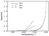
FIG. 2 is a graph showing the comparison of the process temperature and the film forming rate in the preparation of a metal cathode according to various methods in example 1 of the present invention.
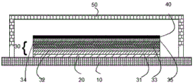
Fig. 3 is a schematic structural diagram of a device D in embodiment 2 of the present invention.
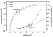
FIG. 4 is a graph showing the variation of luminance and current density of the device D/E/F according to the present invention at different driving voltages in example 2 and comparative example 1.
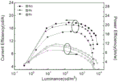
FIG. 5 is a graph showing the variation of current efficiency and power efficiency of the device D/E/F in example 2 of the present invention and the device D/E/F in comparative example 1 at different brightness.
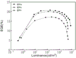
FIG. 6 is a graph showing the variation of External Quantum Efficiency (EQE) of the device D/E/F in example 2 of the present invention and the device D/E/F in comparative example 1 at different brightness.
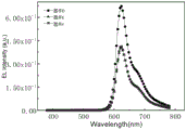
FIG. 7 is a graph showing the spectral distribution of D/E/F at 380nm to 780nm of the devices in example 2 of the present invention and in comparative example 1.
In FIG. 3; 10 is a substrate, 20 is an anode layer, 30 is an organic functional layer, 31 is a hole injection layer, 32 is a hole transport layer, 33 is a light emitting layer, 34 is an electron transport layer, 35 is an electron injection layer, 40 is a cathode layer, and 50 is an encapsulation layer.
Detailed Description
The preparation method of the invention will be further explained with reference to the attached drawings and OLED devices:
the structure of the OLED device prepared by the present invention is as follows, as shown in fig. 3, and includes a substrate 10, an anode layer 20, an organic functional layer 30, a cathode layer 40, and an encapsulation layer 50, wherein:
in the present invention, the cathode layer 40 is used as an electron injection end of the OLED device, and needs to inject electrons into the OLED, so that a lower work function is required, such as Ag; the Ag is prepared by selecting Ag compounds (such as silver oxide and silver carbonate) through an evaporation process; the process temperature for preparing the Ag film layer is 900-1100 ℃, and 1050 ℃ is preferred; the film forming rate of the prepared Ag film layer is 1-20A/s; the thickness of the Ag film layer is 10nm-300nm, preferably 100nm.
In the present invention, the substrate 10 serves as a carrier of the OLED device, and a rigid material such as glass can be selected; the substrate 10 may also be selected from flexible materials such as PI.
In the present invention, the anode layer 20 is used as a hole injection end of the OLED device, and needs to inject holes into the OLED, so that it needs to have a higher work function; a transparent conductive material such as ITO, IZO, FTO, etc. is selected.
In the present invention, the organic functional layer 30, which is a core light emitting unit of the OLED device, includes a hole injection layer 31, a hole transport layer 32, a light emitting layer 33, an electron transport layer 34, and an electron injection layer 35.
In the present invention, the hole injection layer 31 serves as a hole injection unit in the organic functional layer 30, and mainly functions to reduce a barrier for injecting holes from the anode layer 20, so that holes can be efficiently injected from the anode layer 20 into the light-emitting layer 33; the hole injection layer 31 may be made of CuPc, tiOPc, m-MTDATA,2-TNATA, or the like.
In the invention, the hole transport layer 32 is used as a hole transport unit in the organic functional layer 30, and mainly functions to improve the transport rate of holes in the OLED device, and effectively block electrons in the light emitting layer, thereby realizing the maximum recombination of carriers; the hole transport layer 32 may be selected from materials such as TPD, NPB, PVK, spiro-TPD, spiro-NPB, and the like.
In the present invention, the light-emitting layer 33 is used as a light-emitting unit in the organic functional layer 30, and mainly functions to transport electrons and holes and ensure that enough electrons and holes can be recombined to emit light; the material of the light-emitting layer 33 is usually selected from organic small molecule light-emitting materials or complex light-emitting materials, such as Alq3, almq3, TBADN, balq, DPVBi, and the like.
In the present invention, the electron transport layer 34 is used as an electron transport unit in the organic functional layer 30, and mainly functions to improve the electron transport rate in the OLED device and effectively block holes in the light emitting layer, and the material of the electron transport layer 34 is selected from Alq3, almq3, DVPBi, TAZ, OXD, PBD, BND, and the like.
In the present invention, the electron injection layer 35 serves as an electron injection unit in the organic functional layer 30, and mainly functions to reduce the potential barrier for injecting electrons from the cathode layer 40, so that electrons can be efficiently injected from the cathode layer 40 into the light emitting layer 33; the material of the electron injection layer 35 is LiF, mgP, mgF 2 ,Al 2 O 3 And the like.
In the invention, the packaging layer 50 can be packaged by a glass cover plate made of UV glue or a drying agent, or by a film made of silicon nitride/silicon oxide; the packaged OLED device has good water and oxygen resistance.
The preparation method of the Ag electrode comprises the following steps:
feeding: weighing a proper amount of Ag compound, and adding the Ag compound into the cleaned crucible; loading the crucible filled with the Ag compound into an evaporation source cavity, fixing the crucible, and then closing a channel outside the evaporation source cavity;
vacuumizing: starting a vacuum pump, extracting gas in the evaporation cavity, and after 30 minutes, ensuring that the vacuum degree of the evaporation cavity is close to 10 -5 Continuing to extract vacuum and keeping the vacuum degree of the evaporation cavity;
film coating: heating the crucible, heating to 900-1100 ℃, preparing an Ag film layer at a rate of 1-20A/s, keeping the temperature and detecting the film thickness; at this time, the substrate is transferred to the evaporation chamber, the preparation of an Ag film layer having a thickness of 10nm to 300nm, preferably 100nm, on the substrate is started, and when the thickness of the Ag film reaches 100nm, the substrate on which the Ag electrode is evaporated is transferred to the next process.
In the invention, the preparation method of the OLED device comprises the following steps:
1. substrate anode fabrication
Sputtering: preparing a layer of transparent conductive electrode film on the substrate 10 by a magnetron sputtering process to serve as an anode layer of a device;
cleaning and photoetching: cleaning the substrate with the prepared transparent electrode, processing the transparent conductive electrode by processes such as laser etching or photoetching to form a patterned anode layer, and cleaning, drying, UV (ultraviolet) and the like to obtain a clean patterned anode substrate;
2. production of evaporation coating functional layer
Evaporation: sequentially depositing organic functional layers including a hole injection layer, a hole transport layer, a light emitting layer, an electron transport layer and an electron injection layer by an evaporation process, wherein each film layer is sequentially evaporated according to a specific structure;
3. switching an evaporation mask, adding an Ag compound into an evaporation source chamber, vacuumizing, heating, transferring the finished product S3 into the evaporation source chamber, and depositing an Ag electrode; the method comprises the following specific steps:
1) Feeding: weighing a proper amount of Ag compound, and adding the Ag compound into the cleaned crucible; loading the crucible filled with the Ag compound into an evaporation source cavity, fixing the crucible, and then closing a channel outside the evaporation source cavity;
2) Vacuumizing: starting a vacuum pump, extracting gas in the evaporation cavity, and after 30 minutes of extraction, the vacuum degree of the evaporation cavity is close to 10 -5 Continuing to extract vacuum and keeping the vacuum degree of the evaporation cavity;
3) Film coating: heating a crucible, raising the temperature to 900-1100 ℃, preferably 1050 ℃, preparing an Ag film layer at a rate of 1-10A/s, keeping the temperature and detecting the film thickness; at this time, the substrate is transferred to the evaporation chamber, the preparation of an Ag film layer having a thickness of 10nm to 300nm, preferably 100nm, on the substrate is started, and when the thickness of the Ag film reaches 100nm, the substrate on which the Ag electrode is evaporated is transferred to the next process.
4. Preparation of the encapsulation layer
And packaging the evaporated device through processes of dispensing, pressing, UV curing and baking to prepare the closed OLED device.
In order to make the objects, technical solutions and advantages of the present invention more apparent, embodiments of the present invention will be described in detail with reference to the accompanying drawings
This invention may be embodied in many different forms and should not be construed as limited to the embodiments set forth herein. Rather, these embodiments are provided so that this disclosure will be thorough and complete and will fully convey the concept of the invention to those skilled in the art, and the present invention will only be defined by the appended claims. In the drawings, the size and relative sizes of layers and regions may be exaggerated for clarity. It will be understood that when an element such as a layer, region or substrate is referred to as being "formed on" or "disposed on" another element, it can be directly on the other element or intervening elements may also be present. In contrast, when an element is referred to as being "directly formed on" or "directly disposed on" another element, there are no intervening elements present.
Example 1
Example 1 provides the use of Ag in the present invention 2 The preparation method of the Ag electrode prepared by O and the preparation method of the Ag/Al electrode prepared by the traditional process monitor the process temperature and the film forming rate.
Device A uses Ag 2 Preparing an Ag electrode by using O;
preparing an Ag electrode by adopting Ag powder in the device B;
preparing an Al electrode by adopting Al powder in the device C;
the preparation method comprises the following steps:
feeding: 200g of the starting material was weighed (device A selected Ag) 2 O, selecting Ag powder for the device B and Al powder for the device C), and adding the Ag powder and the Al powder into the cleaned crucible; loading the crucible filled with the raw materials into an evaporation source cavity, fixing the crucible, and then closing a channel outside the evaporation source cavity;
vacuumizing and heating: starting a vacuum pump, extracting gas in the evaporation cavity, and after 30 minutes of extraction, the vacuum degree of the evaporation cavity is close to 10 -5 Continuing to extract vacuum and keeping the vacuum degree of the evaporation cavity; when the crucible is heated to 900 ℃, the speed is monitored; the crucible was continuously heated, and the film formation rate of the Ag/Al film at different temperatures was monitored, as shown in FIG. 2.
The test result shows that the device A starts to appear at the temperature of 800 ℃, the rate is relatively stable at the temperature of 950 ℃, and the film forming rate stabilizing temperatures of the devices B and C are 1050 ℃ and 1200 ℃ respectively; meanwhile, the film forming rate of the device A is greatly superior to that of the device B and the device C at the same temperature.
Experiments show that the preparation method of the Ag electrode provided by the invention has relatively low process temperature.
Example 2
Example 2 provides an OLED device D prepared by the Ag electrode preparation method of the present invention, the structure of the device D is shown in fig. 3, and the photoelectric properties of the device D were measured by preparing the device D.
1. The implementation mode is as follows:
in this embodiment, the device D includes a substrate 10, an anode layer 20, an organic functional layer 30, a cathode layer 40, and an encapsulation layer 50, where:
in this example, ag was selected as the cathode layer 40, and the film thickness was 100nm.
In this embodiment, the substrate 10 is made of glass and has a thickness of 0.7mm;
in this embodiment, the anode layer 20 is selected from ITO with a thickness of 150nm;
in the present embodiment, the organic functional layer 30 includes a hole injection layer 31, a hole transport layer 32, a light emitting layer 33, an electron transport layer 34, an electron injection layer 35;
in this embodiment, the hole injection layer 31 is selected from CuPc;
in this embodiment, the hole transport layer 32 is NPB;
in this embodiment, the light-emitting layer 33 is DCJTB;
in this embodiment, alq3 is selected as the electron transport layer 34;
in this embodiment, the electron injection layer 35 is LiF;
in this embodiment, the package layer 50 is a glass cover package with UV glue or desiccant.
The structure of the device D is: ITO (150 nm)/CuPc (15 nm)/NPB (30 nm)/DCJTB (20 nm)/Alq 3 (10 nm)/LiF (15 nm)/Ag (100 nm).
2. Preparation of device D:
the invention provides a preparation method of an OLED device, which comprises the following steps:
s1, substrate anode manufacturing
Sputtering: preparing an ITO film on a glass substrate 10 by a magnetron sputtering process to be used as an anode layer of a device;
cleaning and photoetching: cleaning the prepared ITO substrate, processing an ITO electrode through processes such as laser etching or photoetching to form a patterned anode layer, and cleaning, drying, UV (ultraviolet) and the like to obtain a clean patterned anode substrate;
s2, manufacturing of evaporation coating functional layer
Evaporation: depositing organic functional layers in sequence by an evaporation process, wherein the organic functional layers comprise a hole injection layer, a hole transport layer, a luminescent layer, an electron transport layer and an electron injection layer, and evaporation is carried out on all film layers in sequence according to the structure;
s3, preparation of Ag electrode layer
Feeding: 200g of the starting material (Ag) was weighed 2 O) and adding the mixture into the cleaned crucible; loading the crucible filled with the raw materials into an evaporation source cavity, fixing the crucible, and then closing a channel outside the evaporation source cavity;
vacuumizing and heating: starting a vacuum pump, extracting gas in the evaporation cavity, and after 30 minutes of extraction, the vacuum degree of the evaporation cavity is close to 10 -5 Continuing to extract vacuum and keeping the vacuum degree of the evaporation cavity; and (3) heating the crucible to 900 ℃, starting to monitor the speed, and transmitting the substrate with the Ag electrode plated by vaporization to the next procedure when the thickness of the Ag film reaches 100nm.
S4, preparation of packaging layer
And packaging the evaporated device through processes of dispensing, pressing, UV curing and baking to prepare the closed OLED device.
3. And (3) data testing:
1) The test method comprises the following steps:
testing the electrical performance of the device by using a Keithley 2400 Source Meter current Source, testing the optical performance of the device by using a PR670, and obtaining the brightness, the current efficiency and the power efficiency of the device through testing; drawing a brightness-voltage curve by testing the brightness, the current efficiency and the power efficiency of the device D under different voltages; current efficiency-voltage efficiency-luminance curve; EQE-luminance curve; and (4) a spectrogram for representing the photoelectric property of the device.
2) Test results
The test results of device D of example 2 are shown in table 1.
Table 1: photoelectric test data of device D in embodiment 2 of the invention
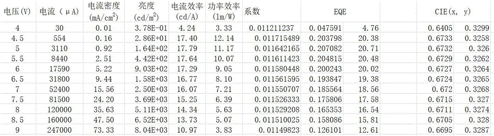
As can be seen from Table 1, device D is at 1-3mA/cm 2 The current density of the high-power LED has better photoelectric performance, the current efficiency can reach 17.5 cd/A, the power efficiency can reach 11 Lm/W, and the external quantum efficiency can reach 20.5 percent. Comparative example 1
To further illustrate the advantages of the present invention, comparative example 1 provides two other electroluminescent devices of similar structure to those of example 2 of the present invention, namely device E and device F, respectively, but not within the scope of the present invention, and the optoelectronic properties of the electroluminescent devices were tested, in comparison with example 2:
1. the concrete structure is as follows:
the device E adopts the traditional process to prepare the Ag electrode, and the structure of the device E is the same as that of the device D.
The device F adopts the traditional process to prepare the Al electrode, and the structure of the device F is the same as that of the device D except the Al electrode, and the specific structure is as follows: ITO (150 nm)/CuPc (15 nm)/NPB (30 nm)/DCJTB (20 nm)/Alq 3 (10 nm)/LiF (15 nm)/Al (100 nm).
2. Preparation of device E/F
The preparation method of the device E/F is different from that of the embodiment 2 in the step S3-material adding, and the other steps are the same;
s3, preparation of Ag electrode layer
Feeding: weighing 200g of raw materials (Ag powder for device E and Al powder for device F), and adding the raw materials into the cleaned crucible; loading the crucible filled with the raw materials into an evaporation source cavity, fixing the crucible, and then closing a channel outside the evaporation source cavity;
3. and (3) data testing:
1) The test method comprises the following steps:
as in example 2.
2) Test results
The test results for device E and device F in comparative example 1 are shown in fig. 4-7, compared to device D.
The following conclusions can be drawn:
1. the device D has higher brightness and current density under the same voltage;
2. the device D has higher current efficiency and power efficiency under the same brightness;
3. the External Quantum Efficiency (EQE) of device D is higher for the same luminance;
4. the spectral performance of the device D is more excellent;
in conclusion, the OLED device prepared by the Ag electrode preparation method has more excellent performances in electrical performance and optical performance.
The foregoing is merely a preferred embodiment of the invention and is not intended to limit the invention in any manner. It should be noted that, for those skilled in the art, without departing from the principle of the present invention, several improvements and modifications can be made, and these improvements and modifications should also be construed as the protection scope of the present invention.
Claims (9)
1. The preparation method of the OLED device containing the Ag electrode is characterized in that the cathode layer is the Ag electrode and is prepared from an Ag compound through an evaporation process;
the preparation method comprises the following specific steps:
s1, preparing a layer of transparent conductive electrode film on a substrate by a magnetron sputtering process to serve as an anode layer of a device;
s2, cleaning the substrate with the prepared transparent electrode, processing the transparent conductive electrode through a laser etching or photoetching process to form a patterned anode layer, and cleaning, drying and performing a UV (ultraviolet) process to obtain a clean patterned anode substrate;
s3, sequentially depositing an organic functional layer by an evaporation process, wherein the organic functional layer comprises but is not limited to a hole injection layer, a hole transport layer, a light emitting layer, an electron transport layer and an electron injection layer, and evaporation is sequentially carried out on all film layers according to a specific structure;
s4, switching an evaporation mask, adding an Ag compound into an evaporation source chamber, vacuumizing, heating, transferring the finished product of S3, and depositing an Ag electrode;
and S5, packaging the evaporated device through dispensing, pressing, UV curing and baking processes to prepare the closed OLED device.
2. The method for preparing an OLED device having an Ag electrode according to claim 1, wherein the Ag compound in step S4 is Ag 2 O or Ag 2 CO 3 。
3. The method for preparing an OLED device with Ag electrode according to claim 1, wherein the specific step of step S4 is as follows,
1) Adding materials; weighing a proper amount of Ag compound, and adding the Ag compound into the cleaned crucible; loading the crucible filled with the Ag compound into an evaporation source cavity, fixing the crucible, and then closing a channel outside the evaporation source cavity;
2) Vacuumizing; starting a vacuum pump, extracting gas in the evaporation cavity, and after 30 minutes of extraction, the vacuum degree of the evaporation cavity is close to 10 -5 Continuing to extract vacuum and keeping the vacuum degree of the evaporation cavity;
3) Coating; heating the crucible to the process temperature, and maintaining the temperature after the evaporation rate of the Ag film layer is stable; and at the moment, transferring the substrate to an evaporation cavity, starting to prepare an Ag electrode on the substrate, and transferring the substrate with the well-evaporated Ag electrode to the next process when the thickness of the Ag film reaches the set film thickness.
4. The method for preparing an OLED device with an Ag electrode according to claim 3, wherein in step 1), ag is selected as the Ag compound 2 O or Ag 2 CO 3 。
5. The method for preparing an OLED device with Ag electrode according to claim 3, wherein the process temperature in step 3) is 900-1100 ℃.
6. The method for preparing an OLED device with Ag electrode according to claim 5, wherein the process temperature in step 3) is 1050 ℃.
7. The method for preparing an OLED device containing an Ag electrode according to claim 3, wherein in the step 3), the Ag film layer evaporation rate is 1-10A/s.
8. The method for preparing an OLED device with Ag electrode according to claim 3, wherein in step 3), the film thickness is set to 10-300 nm.
9. The method for preparing an OLED device with Ag electrode according to claim 8, wherein in step 3), the film thickness is set to 100nm.
Priority Applications (1)
| Application Number | Priority Date | Filing Date | Title |
|---|---|---|---|
| CN202310245539.2A CN115955893B (en) | 2023-03-15 | 2023-03-15 | Preparation method of OLED device containing Ag electrode |
Applications Claiming Priority (1)
| Application Number | Priority Date | Filing Date | Title |
|---|---|---|---|
| CN202310245539.2A CN115955893B (en) | 2023-03-15 | 2023-03-15 | Preparation method of OLED device containing Ag electrode |
Publications (2)
| Publication Number | Publication Date |
|---|---|
| CN115955893A true CN115955893A (en) | 2023-04-11 |
| CN115955893B CN115955893B (en) | 2023-05-30 |
Family
ID=85907045
Family Applications (1)
| Application Number | Title | Priority Date | Filing Date |
|---|---|---|---|
| CN202310245539.2A Active CN115955893B (en) | 2023-03-15 | 2023-03-15 | Preparation method of OLED device containing Ag electrode |
Country Status (1)
| Country | Link |
|---|---|
| CN (1) | CN115955893B (en) |
Cited By (1)
| Publication number | Priority date | Publication date | Assignee | Title |
|---|---|---|---|---|
| CN118364628A (en) * | 2024-04-23 | 2024-07-19 | 华中科技大学 | An electrode optimization method and system based on an OLED device photoelectric coupling simulation model |
Citations (11)
| Publication number | Priority date | Publication date | Assignee | Title |
|---|---|---|---|---|
| JPH0853470A (en) * | 1994-08-10 | 1996-02-27 | Mitsubishi Materials Corp | Organic silver compounds for forming silver thin films by high vapor pressure organometallic chemical vapor deposition |
| JPH0874055A (en) * | 1994-07-07 | 1996-03-19 | Mitsubishi Materials Corp | Method for forming high-purity silver film |
| JPH08283945A (en) * | 1995-04-12 | 1996-10-29 | Mitsubishi Materials Corp | Method for forming low resistance Cu-Ag alloy film and composition for forming low resistance Cu-Ag alloy film |
| CN1359775A (en) * | 2000-12-22 | 2002-07-24 | 中国科学院金属研究所 | Gas-phase laser method and equipment for preparing silver nano-particles |
| CN101222027A (en) * | 2008-01-29 | 2008-07-16 | 清华大学 | A kind of organic light-emitting device and preparation method thereof |
| CN101369635A (en) * | 2008-09-28 | 2009-02-18 | 清华大学 | A kind of inverted OLED display device and preparation method thereof |
| JP2011124468A (en) * | 2009-12-14 | 2011-06-23 | Konica Minolta Holdings Inc | Organic thin film solar cell and method of manufacturing the same |
| CN102208431A (en) * | 2011-03-07 | 2011-10-05 | 昆山维信诺显示技术有限公司 | Organic electroluminescent device and manufacturing method thereof |
| CN103165823A (en) * | 2011-12-13 | 2013-06-19 | 上海大学 | Semi-transparent cathode of OLED device and OLED device |
| CN105700739A (en) * | 2015-12-31 | 2016-06-22 | 奥特路(漳州)光学科技有限公司 | Antibacterial waterproof oil-stain-resisting wear-resistant touch display screen and manufacturing method thereof |
| CN212770958U (en) * | 2020-06-28 | 2021-03-23 | 江西沃格光电股份有限公司 | Covers for electronic equipment and electronic equipment |
-
2023
- 2023-03-15 CN CN202310245539.2A patent/CN115955893B/en active Active
Patent Citations (11)
| Publication number | Priority date | Publication date | Assignee | Title |
|---|---|---|---|---|
| JPH0874055A (en) * | 1994-07-07 | 1996-03-19 | Mitsubishi Materials Corp | Method for forming high-purity silver film |
| JPH0853470A (en) * | 1994-08-10 | 1996-02-27 | Mitsubishi Materials Corp | Organic silver compounds for forming silver thin films by high vapor pressure organometallic chemical vapor deposition |
| JPH08283945A (en) * | 1995-04-12 | 1996-10-29 | Mitsubishi Materials Corp | Method for forming low resistance Cu-Ag alloy film and composition for forming low resistance Cu-Ag alloy film |
| CN1359775A (en) * | 2000-12-22 | 2002-07-24 | 中国科学院金属研究所 | Gas-phase laser method and equipment for preparing silver nano-particles |
| CN101222027A (en) * | 2008-01-29 | 2008-07-16 | 清华大学 | A kind of organic light-emitting device and preparation method thereof |
| CN101369635A (en) * | 2008-09-28 | 2009-02-18 | 清华大学 | A kind of inverted OLED display device and preparation method thereof |
| JP2011124468A (en) * | 2009-12-14 | 2011-06-23 | Konica Minolta Holdings Inc | Organic thin film solar cell and method of manufacturing the same |
| CN102208431A (en) * | 2011-03-07 | 2011-10-05 | 昆山维信诺显示技术有限公司 | Organic electroluminescent device and manufacturing method thereof |
| CN103165823A (en) * | 2011-12-13 | 2013-06-19 | 上海大学 | Semi-transparent cathode of OLED device and OLED device |
| CN105700739A (en) * | 2015-12-31 | 2016-06-22 | 奥特路(漳州)光学科技有限公司 | Antibacterial waterproof oil-stain-resisting wear-resistant touch display screen and manufacturing method thereof |
| CN212770958U (en) * | 2020-06-28 | 2021-03-23 | 江西沃格光电股份有限公司 | Covers for electronic equipment and electronic equipment |
Cited By (1)
| Publication number | Priority date | Publication date | Assignee | Title |
|---|---|---|---|---|
| CN118364628A (en) * | 2024-04-23 | 2024-07-19 | 华中科技大学 | An electrode optimization method and system based on an OLED device photoelectric coupling simulation model |
Also Published As
| Publication number | Publication date |
|---|---|
| CN115955893B (en) | 2023-05-30 |
Similar Documents
| Publication | Publication Date | Title |
|---|---|---|
| TWI599030B (en) | Organic light-emitting element | |
| CN102017799B (en) | Electroluminescence element, display device, and lighting device | |
| WO2013181897A1 (en) | Organic electroluminescent device and preparation method therefor and display device | |
| CN108281559B (en) | A kind of high efficiency, the low phosphorescence Organic Light Emitting Diode that roll-offs | |
| TW200921965A (en) | Organic light emitting device | |
| CN106356464B (en) | A kind of white light organic electroluminescent device and preparation method thereof | |
| CN100470877C (en) | A kind of organic electrophosphorescent device and its preparation method | |
| CN101794864B (en) | Tandem organic light emitting device (OLED) and method for producing same | |
| WO2009021365A1 (en) | Oled and method thereof | |
| CN108565346B (en) | Double-color full-fluorescence white-light OLED device | |
| US20040142098A1 (en) | Using compacted organic materials in making white light emitting oleds | |
| CN115955893B (en) | Preparation method of OLED device containing Ag electrode | |
| CN101916830B (en) | White organic electroluminescent device and preparation method thereof | |
| CN108470838A (en) | A kind of organic electroluminescence device and preparation method thereof | |
| CN113285049A (en) | Method for preparing tungsten trioxide OLED external light extraction layer with high light extraction efficiency by ultrasonic spraying | |
| CN100487945C (en) | Improved organic light-emitting device | |
| Li et al. | Efficient white organic light-emitting device based on a thin layer of hole-transporting host with rubrene dopant | |
| CN104183713A (en) | Top-emission organic light emission diode and preparation method thereof | |
| WO2007026581A1 (en) | Organic electroluminescent device | |
| CN101777630A (en) | White light organic electroluminescent device and preparation method thereof | |
| US20020182307A1 (en) | Organic electroluminescent devices with organic layers deposited at elevated substrate temperatures | |
| KR102186853B1 (en) | An organic-inorganic hybrid perovskite light emitting diode and a method for manufacturing the same | |
| CN106252523B (en) | A kind of new structure for improving organic luminescent device luminous efficiency | |
| CN113725376B (en) | Organic electroluminescent device, method for manufacturing the same and display panel | |
| Srivastava et al. | Fabrication of white organic light-emitting diodes by co-doping of emissive layer |
Legal Events
| Date | Code | Title | Description |
|---|---|---|---|
| PB01 | Publication | ||
| PB01 | Publication | ||
| SE01 | Entry into force of request for substantive examination | ||
| SE01 | Entry into force of request for substantive examination | ||
| GR01 | Patent grant | ||
| GR01 | Patent grant |