CN116189727A - Semiconductor structure, memory and method for manufacturing semiconductor structure - Google Patents
Semiconductor structure, memory and method for manufacturing semiconductor structure Download PDFInfo
- Publication number
- CN116189727A CN116189727A CN202310463781.7A CN202310463781A CN116189727A CN 116189727 A CN116189727 A CN 116189727A CN 202310463781 A CN202310463781 A CN 202310463781A CN 116189727 A CN116189727 A CN 116189727A
- Authority
- CN
- China
- Prior art keywords
- semiconductor layer
- word line
- region
- array
- peripheral
- Prior art date
- Legal status (The legal status is an assumption and is not a legal conclusion. Google has not performed a legal analysis and makes no representation as to the accuracy of the status listed.)
- Granted
Links
Images


Classifications
-
- G—PHYSICS
- G11—INFORMATION STORAGE
- G11C—STATIC STORES
- G11C5/00—Details of stores covered by group G11C11/00
- G11C5/02—Disposition of storage elements, e.g. in the form of a matrix array
- G11C5/025—Geometric lay-out considerations of storage- and peripheral-blocks in a semiconductor storage device
-
- G—PHYSICS
- G11—INFORMATION STORAGE
- G11C—STATIC STORES
- G11C5/00—Details of stores covered by group G11C11/00
- G11C5/06—Arrangements for interconnecting storage elements electrically, e.g. by wiring
- G11C5/063—Voltage and signal distribution in integrated semi-conductor memory access lines, e.g. word-line, bit-line, cross-over resistance, propagation delay
-
- Y—GENERAL TAGGING OF NEW TECHNOLOGICAL DEVELOPMENTS; GENERAL TAGGING OF CROSS-SECTIONAL TECHNOLOGIES SPANNING OVER SEVERAL SECTIONS OF THE IPC; TECHNICAL SUBJECTS COVERED BY FORMER USPC CROSS-REFERENCE ART COLLECTIONS [XRACs] AND DIGESTS
- Y02—TECHNOLOGIES OR APPLICATIONS FOR MITIGATION OR ADAPTATION AGAINST CLIMATE CHANGE
- Y02D—CLIMATE CHANGE MITIGATION TECHNOLOGIES IN INFORMATION AND COMMUNICATION TECHNOLOGIES [ICT], I.E. INFORMATION AND COMMUNICATION TECHNOLOGIES AIMING AT THE REDUCTION OF THEIR OWN ENERGY USE
- Y02D10/00—Energy efficient computing, e.g. low power processors, power management or thermal management
Landscapes
- Engineering & Computer Science (AREA)
- Microelectronics & Electronic Packaging (AREA)
- Semiconductor Memories (AREA)
Abstract
Description
技术领域technical field
本公开属于半导体领域,具体涉及一种半导体结构、存储器及半导体结构的制造方法。The disclosure belongs to the field of semiconductors, and in particular relates to a semiconductor structure, a memory and a method for manufacturing the semiconductor structure.
背景技术Background technique
存储器通常包括半导体层及形成在半导体层上的存储块和外围器件。具体而言,存储块用于存储数据,其可以包括存储单元以及与存储单元相连的字线和位线;外围器件用于控制存储块的读取过程,其可以包括字线驱动器和感测放大器。A memory generally includes a semiconductor layer and memory blocks and peripheral devices formed on the semiconductor layer. Specifically, the memory block is used to store data, which may include memory cells and word lines and bit lines connected to the memory cells; peripheral devices are used to control the read process of the memory block, which may include word line drivers and sense amplifiers .
然而,外围器件和存储块在半导体层上所占据的面积较大,存储器的尺寸有待进一步缩小。另外,存储器的生产工艺较为复杂,存储器的性能也有待提升。However, the area occupied by peripheral devices and storage blocks on the semiconductor layer is large, and the size of the memory needs to be further reduced. In addition, the production process of the memory is relatively complicated, and the performance of the memory needs to be improved.
发明内容Contents of the invention
本公开实施例提供一种半导体结构、存储器及半导体结构的制造方法,至少有利于缩小存储器的尺寸。Embodiments of the present disclosure provide a semiconductor structure, a memory, and a method for manufacturing the semiconductor structure, which at least help reduce the size of the memory.
根据本公开一些实施例,本公开实施例一方面提供一种半导体结构,其中,半导体结构包括:阵列半导体层,具有多个存储块,所述存储块包括多条位线和多条字线;与所述阵列半导体层相键合的外围半导体层,所述外围半导体层包括字线驱动区域和感测放大区域;所述感测放大区域的感测放大器与所述位线电连接,所述字线驱动区域的字线驱动器与所述字线电连接;所述字线驱动区域和所述感测放大区域在所述阵列半导体层上的正投影与至少一个所述存储块在所述阵列半导体层上的正投影至少部分重叠。According to some embodiments of the present disclosure, an embodiment of the present disclosure provides a semiconductor structure on the one hand, wherein the semiconductor structure includes: an array semiconductor layer having a plurality of memory blocks, and the memory blocks include a plurality of bit lines and a plurality of word lines; A peripheral semiconductor layer bonded to the array semiconductor layer, the peripheral semiconductor layer includes a word line drive region and a sense amplifier region; the sense amplifier in the sense amplifier region is electrically connected to the bit line, the The word line driver in the word line drive area is electrically connected to the word line; the orthographic projection of the word line drive area and the sense amplification area on the semiconductor layer of the array is consistent with at least one of the memory blocks in the array The orthographic projections on the semiconductor layer are at least partially overlapping.
根据本公开一些实施例,本公开实施例另一方面还提供一种存储器,包括前述半导体结构。According to some embodiments of the present disclosure, another embodiment of the present disclosure further provides a memory, including the foregoing semiconductor structure.
根据本公开一些实施例,本公开实施例又一方面还提供一种半导体结构的制造方法,半导体结构的制造方法包括:提供阵列半导体层并在所述阵列半导体层上形成第一互连结构,所述阵列半导体层具有多个存储块,所述存储块包括多条位线和多条字线;提供外围半导体层并在所述外围半导体层上形成第二互连结构,所述外围半导体层包括字线驱动区域和感测放大区域;通过所述第一互连结构和所述第二互连结构键合所述阵列半导体层和所述外围半导体层,以使所述字线驱动区域和所述感测放大区域在所述阵列半导体层上的正投影与至少一个所述存储块在所述阵列半导体层上的正投影至少部分重叠,并使所述感测放大区域的感测放大器与所述位线电连接,所述字线驱动区域的字线驱动器与所述字线电连接。According to some embodiments of the present disclosure, an embodiment of the present disclosure further provides a method for manufacturing a semiconductor structure, the method for manufacturing a semiconductor structure includes: providing an array semiconductor layer and forming a first interconnection structure on the array semiconductor layer, The array semiconductor layer has a plurality of memory blocks, the memory block includes a plurality of bit lines and a plurality of word lines; a peripheral semiconductor layer is provided and a second interconnection structure is formed on the peripheral semiconductor layer, the peripheral semiconductor layer Comprising a word line driving area and a sense amplification area; bonding the array semiconductor layer and the peripheral semiconductor layer through the first interconnection structure and the second interconnection structure, so that the word line driving area and the The orthographic projection of the sensing amplifying area on the array semiconductor layer at least partially overlaps the orthographic projection of at least one of the memory blocks on the array semiconductor layer, and the sense amplifier of the sensing amplifying area and the The bit line is electrically connected, and the word line driver in the word line driving area is electrically connected to the word line.
本公开实施例提供的技术方案至少具有以下优点:The technical solutions provided by the embodiments of the present disclosure have at least the following advantages:
半导体结构包括相键合的阵列半导体层和外围半导体层,存储块形成于阵列半导体层上,外围器件形成于外围半导体层上。由于前述两层半导体层层叠设置,因此,有利于降低单个半导体层的面积,并提高在垂直于半导体层上表面的方向上的空间利用率。The semiconductor structure includes a bonded array semiconductor layer and a peripheral semiconductor layer, the memory blocks are formed on the array semiconductor layer, and the peripheral devices are formed on the peripheral semiconductor layer. Since the aforementioned two semiconductor layers are stacked, it is beneficial to reduce the area of a single semiconductor layer and improve the space utilization in a direction perpendicular to the upper surface of the semiconductor layer.
另外,由于存储块和外围器件可以分开制造,因此,生产工艺更简单,产能更高,且有利于提高半导体结构的性能。In addition, since the memory block and peripheral devices can be manufactured separately, the production process is simpler, the production capacity is higher, and it is beneficial to improve the performance of the semiconductor structure.
另外,外围半导体层包括字线驱动区域和感测放大区域,且二者在阵列半导体层上的正投影与至少一个存储块在所述阵列半导体层上的正投影至少部分重叠,从而有利于缩小字线驱动区域和感测放大区域与存储块的距离,进而提高信号传输速率。In addition, the peripheral semiconductor layer includes a word line drive region and a sense amplification region, and the orthographic projections of the two on the array semiconductor layer at least partially overlap with the orthographic projection of at least one memory block on the array semiconductor layer, thereby facilitating shrinking The distance between the word line drive area and the sense amplification area and the memory block is improved to increase the signal transmission rate.
附图说明Description of drawings
此处的附图被并入说明书中并构成本说明书的一部分,示出了符合本公开的实施例,并与说明书一起用于解释本公开的原理。显而易见地,下面描述中的附图仅仅是本公开的一些实施例,对于本领域普通技术人员来讲,在不付出创造性劳动的前提下,还可以根据这些附图获得其他的附图。The accompanying drawings, which are incorporated in and constitute a part of this specification, illustrate embodiments consistent with the disclosure and together with the description serve to explain the principles of the disclosure. Apparently, the drawings in the following description are only some embodiments of the present disclosure, and those skilled in the art can obtain other drawings according to these drawings without creative efforts.
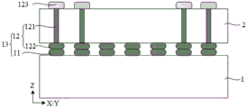
图1示出了本公开实施例提供的一种半导体结构的剖面图。FIG. 1 shows a cross-sectional view of a semiconductor structure provided by an embodiment of the present disclosure.
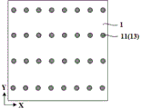
图2示出了本公开实施例提供的阵列半导体层的键合表面的示意图。FIG. 2 shows a schematic diagram of a bonding surface of an array semiconductor layer provided by an embodiment of the present disclosure.
图3示出了本公开实施例提供的外围半导体层的键合表面的示意图。FIG. 3 shows a schematic diagram of a bonding surface of a peripheral semiconductor layer provided by an embodiment of the present disclosure.
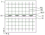
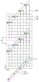
图4示出了本公开实施例提供的半导体结构的第一种局部俯视图。FIG. 4 shows a first partial top view of a semiconductor structure provided by an embodiment of the present disclosure.
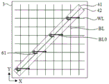
图5示出了本公开实施例提供的半导体结构的第二种局部俯视图。FIG. 5 shows a second partial top view of a semiconductor structure provided by an embodiment of the present disclosure.
图6示出了本公开实施例提供的半导体结构的第三种局部俯视图。FIG. 6 shows a third partial top view of a semiconductor structure provided by an embodiment of the present disclosure.
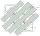
图7示出了本公开实施例提供的半导体结构的第四种局部俯视图。FIG. 7 shows a fourth partial top view of a semiconductor structure provided by an embodiment of the present disclosure.
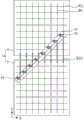
图8示出了本公开实施例提供的半导体结构的第五种局部俯视图。FIG. 8 shows a fifth partial top view of a semiconductor structure provided by an embodiment of the present disclosure.
图9示出了本公开实施例提供的半导体结构的第六种局部俯视图。FIG. 9 shows a sixth partial top view of a semiconductor structure provided by an embodiment of the present disclosure.
图10示出了本公开实施例提供的半导体结构的第七种局部俯视图。FIG. 10 shows a seventh partial top view of a semiconductor structure provided by an embodiment of the present disclosure.
图11示出了本公开实施例提供的半导体结构的第八种局部俯视图。FIG. 11 shows an eighth partial top view of a semiconductor structure provided by an embodiment of the present disclosure.
图12示出了本公开实施例提供的半导体结构的第九种局部俯视图。FIG. 12 shows a ninth partial top view of a semiconductor structure provided by an embodiment of the present disclosure.
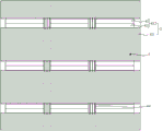
图13示出了本公开实施例提供的半导体结构的第十种局部俯视图。FIG. 13 shows a tenth partial top view of a semiconductor structure provided by an embodiment of the present disclosure.
图14示出了本公开实施例提供的半导体结构的第十一种局部俯视图。FIG. 14 shows an eleventh partial top view of a semiconductor structure provided by an embodiment of the present disclosure.
具体实施方式Detailed ways
由背景技术可知,外围器件和存储块在半导体层上所占据的面积较大,存储器的尺寸有待进一步缩小。存储器的生产工艺较为复杂,存储器的性能也有待提升。经分析发现,主要原因在于:感测放大器和字线驱动器等外围器件与存储块通常形成于同一块半导体层上,因此,半导体层的所需面积较大,且在垂直于半导体层上表面的方向上的空间利用率较低。此外,由于存储块和外围器件的关键工艺不同,性能要求也不同,因此,将两者集成在同一半导体层上的工艺较为复杂,并且可能会导致低产能和低性能。It can be seen from the background art that peripheral devices and memory blocks occupy a relatively large area on the semiconductor layer, and the size of the memory needs to be further reduced. The production process of the memory is relatively complicated, and the performance of the memory needs to be improved. After analysis, it is found that the main reason is that peripheral devices such as sense amplifiers and word line drivers and memory blocks are usually formed on the same semiconductor layer. The space utilization in the direction is low. In addition, since the key process and performance requirements of the memory block and peripheral devices are different, the process of integrating both on the same semiconductor layer is complex and may result in low yield and low performance.
本公开实施例提供一种半导体结构,半导体结构包括阵列半导体层和外围半导体层这两层相互键合的半导体层,存储块形成于阵列半导体层上,外围器件形成于外围半导体层上。由于两层半导体层层叠设置,因此,单个半导体层所需的面积较小,且在垂直于半导体层上表面的方向上的空间利用率较高,从而可以提高半导体结构的集成度。另外,外围半导体层包括字线驱动区域和感测放大区域,且二者在所述阵列半导体层上的正投影与至少一个所述存储块在所述阵列半导体层上的正投影至少部分重叠,即字线驱动区域和感测放大区域与存储块的距离较近,从而有利于提高信号传输速率。An embodiment of the present disclosure provides a semiconductor structure. The semiconductor structure includes two mutually bonded semiconductor layers, an array semiconductor layer and a peripheral semiconductor layer. A memory block is formed on the array semiconductor layer, and peripheral devices are formed on the peripheral semiconductor layer. Since the two semiconductor layers are stacked, the required area of a single semiconductor layer is small, and the space utilization rate in the direction perpendicular to the upper surface of the semiconductor layer is high, so that the integration degree of the semiconductor structure can be improved. In addition, the peripheral semiconductor layer includes a word line driving region and a sensing amplification region, and the orthographic projections of the two on the array semiconductor layer at least partially overlap with the orthographic projection of at least one of the memory blocks on the array semiconductor layer, That is, the distance between the word line driving area and the sensing amplification area and the memory block is relatively close, which is beneficial to increase the signal transmission rate.
下面将结合附图对本公开的各实施例进行详细的阐述。然而,本领域的普通技术人员可以理解,在本公开各实施例中,为了使读者更好地理解本公开实施例而提出了许多技术细节。但是,即使没有这些技术细节和基于以下各实施例的种种变化和修改,也可以实现本公开实施例所要求保护的技术方案。Various embodiments of the present disclosure will be described in detail below with reference to the accompanying drawings. However, those of ordinary skill in the art can understand that, in each embodiment of the present disclosure, many technical details are provided for readers to better understand the embodiments of the present disclosure. However, even without these technical details and various changes and modifications based on the following embodiments, the technical solutions claimed in the embodiments of the present disclosure can be realized.
如图1-图14所示,本公开一实施例提供一种半导体结构,半导体结构包括:阵列半导体层1,具有多个存储块3,存储块3包括多条位线BL和多条字线WL;与阵列半导体层1相键合的外围半导体层2,外围半导体层2包括字线驱动区域42和感测放大区域41;感测放大区域41的感测放大器61与位线BL电连接,字线驱动区域42的字线驱动器62与字线WL电连接;字线驱动区域42和感测放大区域41在阵列半导体层1上的正投影与至少一个存储块3在阵列半导体层1上的正投影至少部分重叠。As shown in FIGS. 1-14 , an embodiment of the present disclosure provides a semiconductor structure. The semiconductor structure includes: an
这样的设计至少具有如下好处:Such a design has at least the following advantages:
第一,将存储块3与感测放大器61、字线驱动器62等外围器件设置在两块不同的半导体层上,有利于缩小单个半导体层的面积。此外,在垂直于半导体层上表面的方向上,半导体层的空间利用率提高。由于存储块3和外围器件分开制造,因此工艺更加简单,生产效率更高,且有利于提高二者的良率和性能。First, the
第二,字线驱动区域42和感测放大区域41在阵列半导体层1上的正投影与至少一个存储块3在阵列半导体层1上的正投影至少部分重叠。这样有利于减小存储块3的位线BL与感测放大器61的距离,以及存储块3的字线WL与字线驱动器62的距离,从而有利于缩短布线长度,缩短延迟时间。Second, the orthographic projection of the word
下面将结合附图对半导体结构进行详细说明。The semiconductor structure will be described in detail below with reference to the accompanying drawings.
半导体结构包括第一方向X、第二方向Y和第三方向Z,第一方向X垂直于第二方向Y,且第一方向X和第二方向Y还与第三方向Z相垂直。其中,第一方向X和第二方向Y可以平行于阵列半导体层1的上表面,第三方向Z可以垂直于阵列半导体层1的上表面。字线WL沿第一方向X延伸,位线BL沿第二方向Y延伸。The semiconductor structure includes a first direction X, a second direction Y and a third direction Z, the first direction X is perpendicular to the second direction Y, and the first direction X and the second direction Y are also perpendicular to the third direction Z. Wherein, the first direction X and the second direction Y may be parallel to the upper surface of the
图1示出了半导体结构的剖面图,参考图1,阵列半导体层1和外围半导体层2可以均为芯片基底或者均为晶圆。阵列半导体层1和外围半导体层2可以通过混合键合的方式连接在一起。阵列半导体层1与外围半导体层2可以通过正面对背面或者正面对正面的方式进行键合。其中,阵列半导体层1形成有存储块3的一面称为正面,外围半导体层2形成有感测放大器61、字线驱动器62等外围器件的一面称为正面。FIG. 1 shows a cross-sectional view of a semiconductor structure. Referring to FIG. 1 , both the
半导体结构还包括互连结构13,互连结构13用于电连接阵列半导体层1与外围半导体层2。互连结构13包括位于阵列半导体层1上的第一互连结构11和位于外围半导体层2上的第二互连结构12。在两个半导体层以正面对正面的方式键合时,第一互连结构11可以为第一焊盘,第二互连结构12可以为第二焊盘122;在两个半导体层以正面对背面的方式键合时,第二互连结构12可以包括第二焊盘122和导电通孔121,导电通孔121可以为穿硅通孔(Through-Silicon Via,TSV)。另外,外围半导体层2还形成有与其他电路或器件连接的数据通道焊垫123(IO pad)。The semiconductor structure further includes an
图2示出了阵列半导体层1的键合表面的示意图,图3示出了外围半导体层2的键合表面的示意图,参考图2-图3,阵列半导体层1和外围半导体层2的键合表面上均设有焊盘以分别作为第一互连结构11和第二互连结构12。在一些实施例中,一个存储块3的位线BL数量范围和字线WL数量范围可以均为900~1100,互连结构13的数量可以等于位线BL和字线WL的数量总和。一个存储块3的面积范围可以为45µm×45µm~55µm×55µm。以互连结构13的数量为2000,存储块3的面积为50µm×50µm为例,则互连结构13的间距约为1.1118µm,该间距符合混合键合的要求。Fig. 2 shows the schematic diagram of the bonding surface of
参考图4-图12,下面将对存储块3进行详细说明。存储块3包括多个阵列排布的存储单元,存储单元可以包括晶体管和电容,字线WL可以与晶体管的栅极相连,位线BL可以与晶体管的源极或漏极相连。在一些实施例中,存储块3可以为存储阵列(array)、存储库(bank),并与全局感测放大器、全局字线驱动器对应电连接。在另一些实施例中,存储块3可以为存储器阵列片(memory array tile,MAT),并与局部感测放大器、局部字线驱动器电连接。Referring to FIGS. 4-12 , the
字线驱动区域42内可以具有多个字线驱动器62,字线驱动器62可以为字线WL提供开启或关闭电压。感测放大区域41内可以具有多个感测放大器61,感测放大器61可以将存储单元传输到位线BL上的数据放大,以保证正确检测存储单元中存储的数据。参考图4-图7,每个字线驱动器62与可以与存储块3内的一条字线WL电连接。参考图8-图12,每个感测放大器61可以与存储块3内的两条位线BL电连接,感测放大器61可以放大两条位线BL上的电压差。需要说明的是,感测放大器61电连接的两条位线BL可以位于同一存储块3内,也可以位于不同的存储块3内,后续将对此进行详细说明。There may be multiple
半导体结构还包括连接线,示例的,至少部分连接线可以在平行于阵列半导体层1的上表面的方向上延伸,从而改变位线BL和字线WL的布局。具体地,参考图4、图6-图7,连接线包括位于外围半导体层2的字线连接线WL0,至少部分字线连接线WL0沿第二方向Y延伸,字线连接线WL0与字线驱动区域42的字线驱动器62电连接,且通过互连结构13与字线WL电连接。参考图8-图12,连接线包括位于外围半导体层2的位线连接线BL0。至少部分位线连接线BL0沿第一方向X延伸,位线连接线BL0与感测放大区域41的感测放大器61电连接,且通过互连结构13与位线BL电连接。也就是说,至少部分位线连接线BL0与位线BL相垂直,至少部分字线连接线WL0与字线WL相垂直,这样能够规范连接线的布局,且减少连接线的长度。The semiconductor structure further includes connecting wires. For example, at least part of the connecting wires may extend in a direction parallel to the upper surface of the
下面将对字线驱动区域42和感测放大区域41的位置关系进行详细说明。The positional relationship between the word
在一些实施例中,参考图4-图14,字线驱动区域42的延伸方向与感测放大区域41的延伸方向相互平行。这是因为每个存储块3都与字线驱动区域42的字线驱动器62以及感测放大区域41的感测放大器61存在电连接关系,因此,将两个区域的延伸方向平行设置可以简化连接线的布局方式,并且为其他的外围区域提供更加充足的空间。In some embodiments, referring to FIGS. 4-14 , the extending direction of the word
具体地,参考图13-图14,字线驱动区域42和感测放大区域41相邻设置,且二者构成第一外围区412;外围半导体层2还包括第二外围区43,第二外围区43内包括地址译码电路或写驱动电路。此外,第二外围区43内还可以包括解码器、IO电路、时钟信号产生电路等外围器件。第二外围区43至少位于第一外围区412的相对两侧。由此,第二外围区43的空间更大,从而能够便于工艺制造,且降低信号干扰。Specifically, referring to FIG. 13-FIG. 14, the word
继续参考图13-图14,外围半导体层2上还具有布线层44,以电连接多个第二外围区43。在一些实施例中,多个第一外围区412间隔设置,从而为第二外围区43之间的布线层44预留位置。至少部分布线层44在阵列半导体层1上的正投影可以与相邻存储块3的间隔区域的正投影相重叠。Continuing to refer to FIGS. 13-14 , there is a
在另一些实施例中,字线驱动区域42和感测放大区域41也可以与感测放大区域41间隔设置。字线驱动区域42的延伸方向也可以与感测放大区域41的延伸方向不同,例如字线驱动区域42的延伸方向垂直于感测放大区域41的延伸方向。In some other embodiments, the word
在一些实施例中,参考图5-图7以及图9-图12,字线驱动区域42的延伸方向可以相对于第一方向X和第二方向Y倾斜,感测放大区域41的延伸方向也可以相对于第一方向X和第二方向Y倾斜。倾斜设置有利于扩大字线驱动区域42的正投影与存储块3的正投影的重叠面积,以及感测放大区域41的正投影与存储块3的正投影的重叠面积,这样可以增大字线驱动器62、感测放大器61以及连接线等结构的工艺窗口,以降低工艺难度。此外,扩大感测放大区域41和字线驱动区域42的空间还有利于降低寄生电容,从而提高半导体结构的性能。In some embodiments, referring to FIG. 5-FIG. 7 and FIG. 9-FIG. 12, the extending direction of the word
例如,字线驱动区域42的延伸方向分别与第一方向X和第二方向Y的夹角可以为
在另一些实施例中,参考图4和图8,字线驱动区域42的延伸方向可以相对于第一方向X或第二方向Y平行,感测放大区域41的延伸方向可以相对于第一方向X或第二方向Y平行。In other embodiments, referring to FIG. 4 and FIG. 8 , the extending direction of the word
举例而言,字线驱动区域42和感测放大区域41的延伸方向均相对于第一方向X平行设置,或者字线驱动区域42和感测放大区域41的延伸方向还可以均相对于第二方向Y平行设置。这样可以保证字线驱动区域42和感测放大区域41的延伸方向的一致性。For example, the extension directions of the word
另外,字线驱动区域42的延伸方向还可以平行于第二方向Y,即平行于多条字线WL的排列方向;且感测放大区域41的延伸方向平行于第一方向X,即平行于多条位线BL的排列方向。如此,字线驱动区域42在阵列半导体层1上的正投影可以与多条字线WL的在阵列半导体层1上正投影至少部分重叠,感测放大区域41在阵列半导体层1上的正投影可以与多条位线BL在阵列半导体层1上的正投影至少部分重叠,这样有利于缩短位线连接线BL0和字线连接线WL0的长度。In addition, the extending direction of the word
参考图4-图7,下面将对字线驱动区域42与存储块3的正投影关系和电连接关系进行举例说明。为了更加清晰地示意字线驱动器62与存储块3的电连接关系,图4-图7未示意感测放大器61及其与存储块3的电连接关系,且图4-图7均为半导体结构的局部示意图。需要说明的是,后续所述的正投影均指位于阵列半导体层1上的正投影。Referring to FIGS. 4-7 , the orthographic relationship and the electrical connection relationship between the word
参考图4-图5,示例一:字线驱动区域42的字线驱动器62与存储块3一一对应电连接,且一字线驱动区域42在阵列半导体层1上的正投影位于对应的一存储块3在阵列半导体层1上的正投影内。即字线驱动区域42与存储块3的正投影关系和电连接关系均是一一对应的。一一对应的方式较为简单,有利于减小字线WL与字线驱动器62的距离,进而提高半导体结构的运行速率。Referring to FIGS. 4-5 , Example 1: the
参考图4,字线驱动区域42的延伸方向可以与第一方向X或第二方向Y平行。参考图5,字线驱动区域42的延伸方向也可以相对于第一方向X和第二方向Y倾斜。也就是说,在示例一中,无论是平行设置还是倾斜设置,字线驱动区域42的正投影均可以与存储块3的正投影相重叠。对比图4-图5可知,在倾斜设置时,多条字线WL的正投影可以与字线驱动区域42的正投影具有重叠关系,由此可以无需设置字线连接线WL0,或者设置较短的字线连接线WL0。示例地,字线驱动区域42可以沿着存储块3的对角线的方向延伸,这样有利于扩大字线驱动器62的空间,以降低寄生电容。在一些实施例中,每一字线WL的正投影均与一字线驱动器62的正投影具有重叠关系。Referring to FIG. 4 , the extending direction of the word
继续参考图4-图5,字线驱动区域42在阵列半导体层1上的正投影覆盖存储块3在阵列半导体层1上的正投影的中心位置。这样可以平衡字线连接线WL0的布局以及降低寄生电容。Continuing to refer to FIGS. 4-5 , the orthographic projection of the word
如图4所示,存储块3可以包括在第二方向Y排布的两个存储子块31,相邻两个字线驱动器62可以与不同存储子块31的字线WL电连接,由此,相邻两个字线驱动器62对应连接的字线连接线WL0无需正对设置,从而有利于降低寄生电容。As shown in FIG. 4, the
在另一些实施例中,参考图6-图7,在第一方向X排布的相邻两个存储块3构成存储组3a,或,在第二方向Y排布的相邻两个存储块3构成存储组3a;一字线驱动区域42在阵列半导体层1上的正投影与一存储组3a的两个存储块3在阵列半导体层1上的正投影至少部分重叠。由于字线驱动区域42的正投影可以与两个存储块3的正投影具有重叠关系,从而有利于为字线驱动器62提供更加充足的空间位置,以降低信号干扰,且简化制造工艺。In some other embodiments, referring to FIGS. 6-7 , two
具体地,参考图6,示例二:字线驱动区域42包括相连的两个第一子区421,且两个第一子区421在阵列半导体层1上的正投影分别与对应存储组3a包括的两个不同存储块3在阵列半导体层1上的正投影至少部分重叠;两个第一子区421的字线驱动器62分别与两个不同存储块3电连接。Specifically, referring to FIG. 6, Example 2: the word
例如,两个第一子区421分别与距离其最近的一个存储块3电连接。也就是说,第一子区421可以与一个存储块3同时具有正投影重叠的关系以及电连接关系。这样有利于简化字线连接线WL0的布局方式,提高信号传输速率。For example, the two first sub-areas 421 are electrically connected to the
具体而言,每个存储块3包括两个存储子块31,两个存储子块31可以在第一方向X或第二方向Y上排列。字线驱动区域42的两个第一子区421的字线驱动器62分别与两个不同存储块3中的一个存储子块31对应电连接,且第一子区421的正投影与对应存储子块31的正投影至少部分重叠。也就是说,一个第一子区421的字线驱动器62与一个存储子块31的字线WL电连接,且一个第一子区421的正投影与一个存储子块31的正投影具有重叠关系。Specifically, each
继续参考图6,第一子区421内的多个字线驱动器62可以等间距排列,多条字线连接线WL0的长度可以相同,这样可以提高半导体结构的均一性,避免产生不同的延迟时间。另外,多条字线连接线WL0还可以错开设置,即多条字线连接线WL0在第一方向X不是正对正对关系,这样可以降低寄生电容。Continuing to refer to FIG. 6, multiple
参考图7,示例三:字线驱动区域42包括相连的两个第一子区421,且两个第一子区421在阵列半导体层1上的正投影分别与对应存储组3a包括的两个不同存储块3在阵列半导体层1上的正投影至少部分重叠;两个第一子区421的字线驱动器62均与对应存储组3a中的一个存储块3电连接。即,虽然字线驱动区域42的正投影可以与两个存储块3的正投影具有重叠关系,但字线驱动区域42的字线驱动器62可以只与其中一个存储块3电连接。Referring to FIG. 7 , Example 3: the word
需要说明的是,在示例二和示例三中,字线驱动区域42的延伸方向可以相对于第一方向X和第二方向Y倾斜,即字线驱动区域42的延伸方向不同于第一方向X和第二方向Y,以保证字线驱动区域42可以横跨两个存储块3。It should be noted that, in Example 2 and Example 3, the extending direction of the word
对比示例二和示例三可知,在字线驱动区域42与两个存储块3的字线WL均存在电连接关系时,字线连接线WL0的长度更短,且字线连接线WL0之间的正对面积更小,这样可以缩短延迟时间,减小寄生电容。Comparing Example 2 and Example 3, it can be seen that when the word
参考图8-图12,下面将对感测放大区域41与存储块3的投影关系和电连接关系进行举例说明。为了更加清晰地示意感测放大区域41与存储块3的电连接关系,图8-图12未示意字线驱动器62及其与存储块3的电连接关系。图8-图12均为半导体结构的局部示意图。Referring to FIGS. 8-12 , the projection relationship and electrical connection relationship between the
参考图8-图9,示例四:感测放大区域41的感测放大器61与存储块3一一对应电连接,且一感测放大区域41在阵列半导体层1上的正投影位于对应的一存储块3在阵列半导体层1上的正投影内。即感测放大区域41与存储块3的正投影关系和电连接关系均是一一对应的。一一对应的连接方式较为简单,且有利于缩小位线BL与感测放大器61的距离,从而提高半导体结构的运行速率。Referring to FIGS. 8-9 , Example 4: The
参考图8,感测放大区域41的延伸方向可以与第一方向X或第二方向Y平行。参考图9,感测放大区域41的延伸方向可以相对于第一方向X和第二方向Y倾斜。例如,感测放大区域41可以沿着存储块3的对角线的方向延伸,这样有利于扩大感测放大区域41的空间,以降低寄生电容。此外,较多位线BL的正投影可以与感测放大区域41的正投影具有重叠,以简化位线连接线BL0的布局。Referring to FIG. 8 , the extending direction of the
继续参考图8-图9,感测放大区域41在阵列半导体层1上的正投影覆盖存储块3在阵列半导体层1上的正投影的中心位置。这样可以平衡位线连接线BL0的布局以及降低寄生电容。Continuing to refer to FIGS. 8-9 , the orthographic projection of the
参考图8,感测放大器61的正投影可以位于与其电连接的两条位线BL的正投影之间,这样有利于减小位线连接线BL0的长度。此外,参考图9,感测放大器61还可以位于与其电连接的两条位线BL的同一侧。Referring to FIG. 8 , the orthographic projection of the
在另一些实施例中,参考图10-图12,在第一方向X排布的相邻两个存储块3构成存储组3a,或,在第二方向Y排布的相邻两个存储块3构成存储组3a;一感测放大区域41在阵列半导体层1上的正投影与一存储组3a的两个存储块3在阵列半导体层1上的正投影至少部分重叠。由于感测放大区域41的正投影可以与两个存储块3的正投影具有重叠关系,从而有利于为感测放大区域41提供更加充足的空间位置,以降低信号干扰,且简化制造工艺。In some other embodiments, referring to FIGS. 10-12 , two
具体地,参考图10,示例五:感测放大区域41包括相连的两个第二子区411,且两个第二子区411在阵列半导体层1上的正投影分别与对应存储组3a包括的两个不同存储块3在阵列半导体层1上的正投影至少部分重叠,两个第二子区411的感测放大器61分别与两个不同存储块3电连接。Specifically, referring to FIG. 10 , example five: the sensing
例如,两个第二子区411分别与距离其最近的一个存储块3电连接。也就是说,第二子区411可以与一个存储块3同时具有正投影重叠的关系以及电连接关系。这样有利于简化位线连接线BL0的布局方式,提高信号传输速率。For example, the two
具体而言,每个存储块3包括两个存储子块31,两个存储子块31可以在第一方向X或第二方向Y上排列。感测放大区域41的两个第二子区411分别与两个不同存储块3中的一个存储子块31对应电连接,且第二子区411的正投影与对应存储子块31的正投影至少部分重叠。也就是说,一个第二子区411的感测放大器61与一个存储子块31的位线BL对应电连接,且一个第二子区411的正投影与对应的一个存储子块31的正投影具有重叠关系。Specifically, each
参考图11,示例六:感测放大区域41包括相连的两个第二子区411,且两个第二子区411在阵列半导体层1上的正投影分别与对应存储组3a包括的两个不同存储块3在阵列半导体层1上的正投影至少部分重叠,两个第二子区411的感测放大器61均与对应存储组3中的一个存储块3电连接。即,虽然感测放大区域41的正投影可以与两个存储块3的正投影具有重叠关系,但感测放大区域41的感测放大器61可以只与其中一个存储块3电连接。Referring to FIG. 11, example six: the
对比示例五和示例六可知,在感测放大区域41与两个存储块3的位线BL均存在电连接关系时,位线连接线BL0的长度更短,且位线连接线BL0之间的正对面积更小,这样可以缩短延迟时间,减小寄生电容。Comparing Example 5 and Example 6, it can be seen that when the
参考图12,示例七:一个感测放大区域41的感测放大器61与对应存储组3a中的两个存储块3电连接。即一个感测放大区域41和两个与其具有正投影重叠关系的存储块3中的所有位线BL电连接。Referring to FIG. 12 , example seven: the
举例而言,存储组3a的两个存储块3在第二方向Y上排列。每一感测放大器61电连接两条不同存储块3的位线BL,与同一感测放大器61电连接的两条位线BL在第二方向Y上对齐。这样可以减少感测放大器61的数量,从而为第二外围区43的外围器件以及布线层44(参考图13-图14)等结构提供更充足的空间。For example, two
需要说明的是,在示例五至示例七中,感测放大区域41的延伸方向可以相对于第一方向X和第二方向Y倾斜,即感测放大区域41的延伸方向不同于第一方向X和第二方向Y,以保证感测放大区域41可以横跨两个存储块3。It should be noted that, in Example 5 to Example 7, the extension direction of the
值得注意的是,在不矛盾的前提下,“字线驱动区域42与存储块3的正投影关系、电连接关系”可以与“感测放大区域41与存储块3的正投影关系、电连接关系”相互组合。It is worth noting that, under the premise of no contradiction, "the orthographic relationship and electrical connection relationship between the word
举例而言,一字线驱动区域42和一感测放大区域41均与一存储块3存在正投影重叠关系和电连接关系。或者,一字线驱动区域42和一感测放大区域41均与两个存储块3存在正投影重叠关系和电连接关系。这样有利于提高半导体结构的均一性,有利于减小连接线长度,从而为第二外围区43提供更加充足的空间。值得注意的是,本公开实施例并不限于上述两种组合方案。即,示例一至示例三的各方案可以与示例四至示例七的各方案进行两两组合。For example, both a word
综上所述,本公开实施例中将存储块3和外围器件设置在两块不同的半导体层上并键合设置,从而有利于缩小半导体层的面积,并且有利于提高生产效率和半导体结构的性能。字线驱动区域42和感测放大区域41在阵列半导体层1上的正投影与至少一个存储块3在阵列半导体层1上的正投影至少部分重叠,这样有利于减小连接线的长度,缩短延迟时间。To sum up, in the embodiment of the present disclosure, the
本公开实施例还提供一种存储器,存储器包括前述实施例提供的半导体结构,有关此半导体结构的详细说明可以参考前述实施例。存储器可以为动态随机存取存储器(Dynamic Random Access Memory,DRAM)、静态随机存储器(Static Random-AccessMemory,SRAM)、高带宽存储器(High Bandwidth Memory,HBM)等存储器。An embodiment of the present disclosure further provides a memory, and the memory includes the semiconductor structure provided in the foregoing embodiments. For detailed descriptions of the semiconductor structure, reference may be made to the foregoing embodiments. The memory may be a memory such as a dynamic random access memory (Dynamic Random Access Memory, DRAM), a static random access memory (Static Random-Access Memory, SRAM), a high bandwidth memory (High Bandwidth Memory, HBM), and the like.
本公开实施例还提供一种半导体结构的制造方法,此制造方法可以制造前述实施例提供的半导体结构,有关此半导体结构的详细说明可以参考前述实施例。Embodiments of the present disclosure also provide a method for manufacturing a semiconductor structure. The manufacturing method can manufacture the semiconductor structure provided in the foregoing embodiments. For detailed descriptions of the semiconductor structure, reference can be made to the foregoing embodiments.
参考图1,制造方法包括:提供阵列半导体层1并在阵列半导体层1上形成第一互连结构11。示例地,通过图形化工艺和沉积工艺形成第一焊盘以作为第一互连结构11。阵列半导体层1还可以具有介质层,第一互连结构11的上表面可以与介质层的上表面齐平。阵列半导体层还具有多个存储块3(参考图4-图14),存储块3包括多条位线BL和多条字线WL。Referring to FIG. 1 , the manufacturing method includes: providing an
提供外围半导体层2并在外围半导体层2上形成第二互连结构12。示例地,通过图形化工艺和沉积工艺形成第二焊盘122和导电通孔121以作为第二互连结构12。在另一些实施例中,也可以只形成第二焊盘122以作为第二互连结构12。外围半导体层2还可以具有介质层,第二互连结构12的上表面可以与介质层的上表面齐平。外围半导体层2还包括字线驱动区域42和感测放大区域41。A
通过第一互连结构11和第二互连结构12键合阵列半导体层1和外围半导体层2,以使字线驱动区域42和感测放大区域41在阵列半导体层1上的正投影与至少一个存储块3在阵列半导体层1上的正投影至少部分重叠,并使感测放大区域41的感测放大器61与位线BL电连接,字线驱动区域42的字线驱动器62与字线WL电连接。示例地,采用混合键合的方式,使得第一互连结构11与第二互连结构12对准且键合,使得阵列半导体层1上的介质层与外围半导体层2上的介质层对准且键合。The
在另一些实施例中,还可以采用熔融键合的方式实现两个半导体层的键合。即,第一互连结构11和第二互连结构12可以均为凸设于半导体层表面的焊球。In some other embodiments, the bonding of the two semiconductor layers can also be achieved by means of fusion bonding. That is, both the
在本说明书的描述中,参考术语 “一些实施例”、“示例地”等的描述意指结合该实施例或示例描述的具体特征、结构、材料或者特点包含于本公开的至少一个实施例或示例中。在本说明书中,对上述术语的示意性表述不必须针对的是相同的实施例或示例。而且,描述的具体特征、结构、材料或者特点可以在任一个或多个实施例或示例中以合适的方式结合。此外,在不相互矛盾的情况下,本领域的技术人员可以将本说明书中描述的不同实施例或示例以及不同实施例或示例的特征进行结合和组合。In the description of this specification, descriptions with reference to the terms "some embodiments", "exemplarily" and the like mean that specific features, structures, materials or characteristics described in connection with the embodiments or examples are included in at least one embodiment or embodiment of the present disclosure. example. In this specification, the schematic representations of the above terms are not necessarily directed to the same embodiment or example. Furthermore, the described specific features, structures, materials or characteristics may be combined in any suitable manner in any one or more embodiments or examples. In addition, those skilled in the art can combine and combine different embodiments or examples and features of different embodiments or examples described in this specification without conflicting with each other.
尽管上面已经示出和描述了本公开的实施例,可以理解的是,上述实施例是示例性的,不能理解为对本公开的限制,本领域的普通技术人员在本公开的范围内可以对上述实施例进行变化、修改、替换和变型,故但凡依本公开的权利要求和说明书所做的变化或修饰,皆应属于本公开专利涵盖的范围之内。Although the embodiments of the present disclosure have been shown and described above, it can be understood that the above embodiments are exemplary and should not be construed as limitations on the present disclosure, and those skilled in the art can understand the above-mentioned embodiments within the scope of the present disclosure. The embodiments are changed, modified, replaced and modified, so any changes or modifications made according to the claims and description of the present disclosure shall fall within the scope covered by the patent of the present disclosure.
Claims (15)
Priority Applications (1)
| Application Number | Priority Date | Filing Date | Title |
|---|---|---|---|
| CN202310463781.7A CN116189727B (en) | 2023-04-26 | 2023-04-26 | Semiconductor structure, memory and method of manufacturing semiconductor structure |
Applications Claiming Priority (1)
| Application Number | Priority Date | Filing Date | Title |
|---|---|---|---|
| CN202310463781.7A CN116189727B (en) | 2023-04-26 | 2023-04-26 | Semiconductor structure, memory and method of manufacturing semiconductor structure |
Publications (2)
| Publication Number | Publication Date |
|---|---|
| CN116189727A true CN116189727A (en) | 2023-05-30 |
| CN116189727B CN116189727B (en) | 2023-09-19 |
Family
ID=86444633
Family Applications (1)
| Application Number | Title | Priority Date | Filing Date |
|---|---|---|---|
| CN202310463781.7A Active CN116189727B (en) | 2023-04-26 | 2023-04-26 | Semiconductor structure, memory and method of manufacturing semiconductor structure |
Country Status (1)
| Country | Link |
|---|---|
| CN (1) | CN116189727B (en) |
Cited By (3)
| Publication number | Priority date | Publication date | Assignee | Title |
|---|---|---|---|---|
| WO2025139323A1 (en) * | 2023-12-29 | 2025-07-03 | 长鑫科技集团股份有限公司 | Memory |
| EP4668269A1 (en) * | 2024-06-20 | 2025-12-24 | Samsung Electronics Co., Ltd. | Memory device |
| WO2026081605A1 (en) * | 2024-10-18 | 2026-04-23 | 长鑫科技集团股份有限公司 | Semiconductor device and preparation method for semiconductor device |
Citations (12)
| Publication number | Priority date | Publication date | Assignee | Title |
|---|---|---|---|---|
| US5768174A (en) * | 1995-12-06 | 1998-06-16 | Samsung Electronics Co., Ltd. | Integrated circuit memory devices having metal straps to improve word line driver reliability |
| JP2003059289A (en) * | 2001-06-04 | 2003-02-28 | Toshiba Corp | Semiconductor memory device |
| US20110169062A1 (en) * | 2010-01-08 | 2011-07-14 | Elpida Memory, Inc. | Semiconductor device and method of fabricating the same |
| US20140246725A1 (en) * | 2013-03-04 | 2014-09-04 | Samsung Electronics Co., Ltd. | Integrated Circuit Memory Devices Including Parallel Patterns in Adjacent Regions |
| CN110890372A (en) * | 2018-09-07 | 2020-03-17 | 三星电子株式会社 | Semiconductor memory device and method of manufacturing the same |
| CN112599528A (en) * | 2020-12-14 | 2021-04-02 | 武汉新芯集成电路制造有限公司 | Semiconductor device and method of making the same |
| CN114121968A (en) * | 2020-08-25 | 2022-03-01 | 三星电子株式会社 | Three-dimensional semiconductor memory device |
| CN114747009A (en) * | 2020-01-28 | 2022-07-12 | 桑迪士克科技有限责任公司 | Joint assembly with vertical power and control signal connections adjacent to sense amplifier region and method of forming same |
| CN115410617A (en) * | 2022-09-19 | 2022-11-29 | 长鑫存储技术有限公司 | Word line driver and memory device |
| US20230055147A1 (en) * | 2021-08-17 | 2023-02-23 | Samsung Electronics Co., Ltd. | Semiconductor memory device |
| US20230060149A1 (en) * | 2021-08-31 | 2023-03-02 | Yangtze Memory Technologies Co., Ltd. | Memory devices having vertical transistors and methods for forming the same |
| CN115995248A (en) * | 2021-10-20 | 2023-04-21 | 爱思开海力士有限公司 | Storage device and method of operating same |
-
2023
- 2023-04-26 CN CN202310463781.7A patent/CN116189727B/en active Active
Patent Citations (12)
| Publication number | Priority date | Publication date | Assignee | Title |
|---|---|---|---|---|
| US5768174A (en) * | 1995-12-06 | 1998-06-16 | Samsung Electronics Co., Ltd. | Integrated circuit memory devices having metal straps to improve word line driver reliability |
| JP2003059289A (en) * | 2001-06-04 | 2003-02-28 | Toshiba Corp | Semiconductor memory device |
| US20110169062A1 (en) * | 2010-01-08 | 2011-07-14 | Elpida Memory, Inc. | Semiconductor device and method of fabricating the same |
| US20140246725A1 (en) * | 2013-03-04 | 2014-09-04 | Samsung Electronics Co., Ltd. | Integrated Circuit Memory Devices Including Parallel Patterns in Adjacent Regions |
| CN110890372A (en) * | 2018-09-07 | 2020-03-17 | 三星电子株式会社 | Semiconductor memory device and method of manufacturing the same |
| CN114747009A (en) * | 2020-01-28 | 2022-07-12 | 桑迪士克科技有限责任公司 | Joint assembly with vertical power and control signal connections adjacent to sense amplifier region and method of forming same |
| CN114121968A (en) * | 2020-08-25 | 2022-03-01 | 三星电子株式会社 | Three-dimensional semiconductor memory device |
| CN112599528A (en) * | 2020-12-14 | 2021-04-02 | 武汉新芯集成电路制造有限公司 | Semiconductor device and method of making the same |
| US20230055147A1 (en) * | 2021-08-17 | 2023-02-23 | Samsung Electronics Co., Ltd. | Semiconductor memory device |
| US20230060149A1 (en) * | 2021-08-31 | 2023-03-02 | Yangtze Memory Technologies Co., Ltd. | Memory devices having vertical transistors and methods for forming the same |
| CN115995248A (en) * | 2021-10-20 | 2023-04-21 | 爱思开海力士有限公司 | Storage device and method of operating same |
| CN115410617A (en) * | 2022-09-19 | 2022-11-29 | 长鑫存储技术有限公司 | Word line driver and memory device |
Cited By (3)
| Publication number | Priority date | Publication date | Assignee | Title |
|---|---|---|---|---|
| WO2025139323A1 (en) * | 2023-12-29 | 2025-07-03 | 长鑫科技集团股份有限公司 | Memory |
| EP4668269A1 (en) * | 2024-06-20 | 2025-12-24 | Samsung Electronics Co., Ltd. | Memory device |
| WO2026081605A1 (en) * | 2024-10-18 | 2026-04-23 | 长鑫科技集团股份有限公司 | Semiconductor device and preparation method for semiconductor device |
Also Published As
| Publication number | Publication date |
|---|---|
| CN116189727B (en) | 2023-09-19 |
Similar Documents
| Publication | Publication Date | Title |
|---|---|---|
| CN116189727A (en) | Semiconductor structure, memory and method for manufacturing semiconductor structure | |
| CN111292784A (en) | Integrated assembly including vertically stacked levels | |
| US8710570B2 (en) | Semiconductor device having vertical channel | |
| TW202111923A (en) | Non-volatile memory device utilizing dummy memory block as pool capacitor | |
| KR20230025474A (en) | Buried signal wires for memory applications | |
| US20240260254A1 (en) | Semiconductor device with vertical body contact and methods for manufacturing the same | |
| TW202412272A (en) | Semiconductor structure and memory | |
| JP2025508480A (en) | MEMORY DEVICE AND METHODS FOR FORMING SAME - Patent application | |
| CN114783481B (en) | Integrated components | |
| KR20240146854A (en) | Semiconductor device including backside transistors | |
| CN114420180A (en) | Dynamic random access memory and forming method thereof | |
| CN114765038A (en) | Integrated assembly and semiconductor memory device | |
| US6317358B1 (en) | Efficient dual port DRAM cell using SOI technology | |
| CN115835625A (en) | Semiconductor structure, manufacturing method thereof and memory system | |
| WO2022228281A1 (en) | Three-dimensional memory, chip packaging structure, and electronic device | |
| CN119136532B (en) | semiconductor structure | |
| JP2002217385A (en) | Semiconductor integrated circuit device | |
| US20260075830A1 (en) | Memory device including block selection circuit | |
| US12444448B2 (en) | Memory device with memory array connected to circuits in different stacked substrates | |
| US20260094627A1 (en) | Memory device, fabrication method thereof and system | |
| US20260024560A1 (en) | Semiconductor memory device | |
| US20250309093A1 (en) | Power rail in stacked fet devices | |
| TW202517010A (en) | Memory device | |
| WO2024198036A1 (en) | Semiconductor structure, semiconductor forming method, and memory | |
| TW202605815A (en) | Mram circuit and layout |
Legal Events
| Date | Code | Title | Description |
|---|---|---|---|
| PB01 | Publication | ||
| PB01 | Publication | ||
| SE01 | Entry into force of request for substantive examination | ||
| SE01 | Entry into force of request for substantive examination | ||
| GR01 | Patent grant | ||
| GR01 | Patent grant |