CN116419082A - Realization method of high dynamic imaging and its device, image processing system - Google Patents
Realization method of high dynamic imaging and its device, image processing system Download PDFInfo
- Publication number
- CN116419082A CN116419082A CN202111657558.3A CN202111657558A CN116419082A CN 116419082 A CN116419082 A CN 116419082A CN 202111657558 A CN202111657558 A CN 202111657558A CN 116419082 A CN116419082 A CN 116419082A
- Authority
- CN
- China
- Prior art keywords
- unit
- voltage
- signal
- column
- pixel
- Prior art date
- Legal status (The legal status is an assumption and is not a legal conclusion. Google has not performed a legal analysis and makes no representation as to the accuracy of the status listed.)
- Pending
Links
Images


Classifications
-
- H—ELECTRICITY
- H04—ELECTRIC COMMUNICATION TECHNIQUE
- H04N—PICTORIAL COMMUNICATION, e.g. TELEVISION
- H04N9/00—Details of colour television systems
- H04N9/77—Circuits for processing the brightness signal and the chrominance signal relative to each other, e.g. adjusting the phase of the brightness signal relative to the colour signal, correcting differential gain or differential phase
-
- H—ELECTRICITY
- H04—ELECTRIC COMMUNICATION TECHNIQUE
- H04N—PICTORIAL COMMUNICATION, e.g. TELEVISION
- H04N25/00—Circuitry of solid-state image sensors [SSIS]; Control thereof
- H04N25/70—SSIS architectures; Circuits associated therewith
- H04N25/76—Addressed sensors, e.g. MOS or CMOS sensors
- H04N25/77—Pixel circuitry, e.g. memories, A/D converters, pixel amplifiers, shared circuits or shared components
- H04N25/771—Pixel circuitry, e.g. memories, A/D converters, pixel amplifiers, shared circuits or shared components comprising storage means other than floating diffusion
-
- H—ELECTRICITY
- H04—ELECTRIC COMMUNICATION TECHNIQUE
- H04N—PICTORIAL COMMUNICATION, e.g. TELEVISION
- H04N23/00—Cameras or camera modules comprising electronic image sensors; Control thereof
- H04N23/70—Circuitry for compensating brightness variation in the scene
- H04N23/741—Circuitry for compensating brightness variation in the scene by increasing the dynamic range of the image compared to the dynamic range of the electronic image sensors
-
- H—ELECTRICITY
- H04—ELECTRIC COMMUNICATION TECHNIQUE
- H04N—PICTORIAL COMMUNICATION, e.g. TELEVISION
- H04N25/00—Circuitry of solid-state image sensors [SSIS]; Control thereof
- H04N25/50—Control of the SSIS exposure
- H04N25/57—Control of the dynamic range
-
- H—ELECTRICITY
- H04—ELECTRIC COMMUNICATION TECHNIQUE
- H04N—PICTORIAL COMMUNICATION, e.g. TELEVISION
- H04N25/00—Circuitry of solid-state image sensors [SSIS]; Control thereof
- H04N25/50—Control of the SSIS exposure
- H04N25/57—Control of the dynamic range
- H04N25/58—Control of the dynamic range involving two or more exposures
- H04N25/581—Control of the dynamic range involving two or more exposures acquired simultaneously
-
- H—ELECTRICITY
- H04—ELECTRIC COMMUNICATION TECHNIQUE
- H04N—PICTORIAL COMMUNICATION, e.g. TELEVISION
- H04N25/00—Circuitry of solid-state image sensors [SSIS]; Control thereof
- H04N25/50—Control of the SSIS exposure
- H04N25/57—Control of the dynamic range
- H04N25/59—Control of the dynamic range by controlling the amount of charge storable in the pixel, e.g. modification of the charge conversion ratio of the floating node capacitance
-
- H—ELECTRICITY
- H04—ELECTRIC COMMUNICATION TECHNIQUE
- H04N—PICTORIAL COMMUNICATION, e.g. TELEVISION
- H04N25/00—Circuitry of solid-state image sensors [SSIS]; Control thereof
- H04N25/70—SSIS architectures; Circuits associated therewith
- H04N25/76—Addressed sensors, e.g. MOS or CMOS sensors
- H04N25/77—Pixel circuitry, e.g. memories, A/D converters, pixel amplifiers, shared circuits or shared components
-
- H—ELECTRICITY
- H04—ELECTRIC COMMUNICATION TECHNIQUE
- H04N—PICTORIAL COMMUNICATION, e.g. TELEVISION
- H04N25/00—Circuitry of solid-state image sensors [SSIS]; Control thereof
- H04N25/70—SSIS architectures; Circuits associated therewith
- H04N25/76—Addressed sensors, e.g. MOS or CMOS sensors
- H04N25/78—Readout circuits for addressed sensors, e.g. output amplifiers or A/D converters
-
- H—ELECTRICITY
- H04—ELECTRIC COMMUNICATION TECHNIQUE
- H04N—PICTORIAL COMMUNICATION, e.g. TELEVISION
- H04N25/00—Circuitry of solid-state image sensors [SSIS]; Control thereof
- H04N25/70—SSIS architectures; Circuits associated therewith
- H04N25/76—Addressed sensors, e.g. MOS or CMOS sensors
Landscapes
- Engineering & Computer Science (AREA)
- Multimedia (AREA)
- Signal Processing (AREA)
- Transforming Light Signals Into Electric Signals (AREA)
- Solid State Image Pick-Up Elements (AREA)
Abstract
本发明提供一种高动态成像的实现方法及其装置、图像处理系统,其中,所述高动态成像装置包括图像传感器,所述图像传感器中的像素阵列,包括多个像素单元;列处理单元,包括增益控制单元和模数转换单元;所述像素单元包括两个具有不同感光灵敏度的光电转换单元;所述增益控制单元,用于根据所述像素单元输出的信号电压判断图像所处的亮度范围,并根据所述亮度范围选择所述像素单元中进行信号转换的光电转换单元、所述像素单元的电荷‑电压转换增益和所述列处理单元的电压增益。本发明提供的高动态成像的实现方法及其装置、图像处理可以只读出一次信号电压,缩短行读出时间,进而提高帧率。

The present invention provides a method for realizing high dynamic imaging, its device, and an image processing system, wherein the high dynamic imaging device includes an image sensor, and a pixel array in the image sensor includes a plurality of pixel units; a column processing unit, Including a gain control unit and an analog-to-digital conversion unit; the pixel unit includes two photoelectric conversion units with different photosensitivity; the gain control unit is used to judge the brightness range of the image according to the signal voltage output by the pixel unit , and select the photoelectric conversion unit for signal conversion in the pixel unit, the charge-voltage conversion gain of the pixel unit, and the voltage gain of the column processing unit according to the brightness range. The realization method of high dynamic imaging provided by the present invention, its device, and image processing can only read out the signal voltage once, shorten the line readout time, and further improve the frame rate.
Description
技术领域technical field
本发明涉及图像传感器技术领域,尤其涉及一种高动态成像的实现方法及其装置、图像处理系统。The invention relates to the technical field of image sensors, in particular to a method for realizing high dynamic imaging, a device thereof, and an image processing system.
背景技术Background technique
高动态范围图像(High-Dynamic Range,简称HDR),相比普通的图像,可以提供更多的动态范围和图像细节,根据不同的曝光时间的LDR(Low-Dynamic Range)图像,利用每个曝光时间相对应最佳细节的LDR图像来合成最终HDR图像,能够更好的反映出真实环境中的视觉效果。High-Dynamic Range (HDR) images can provide more dynamic range and image details than ordinary images. According to LDR (Low-Dynamic Range) images with different exposure times, each exposure Time corresponds to the LDR image with the best details to synthesize the final HDR image, which can better reflect the visual effect in the real environment.
CMOS图像传感器(CMOS image sensor,CIS)广泛应用到手机、监控安防、机器视觉、消费电子等各个领域,应用领域的拓展对CIS的性能指标提出了更高的要求。动态范围(dynamic range)是CIS的重要指标之一,在监控安防、自动驾驶等较为复杂的应用场景中尤为关键。CMOS image sensor (CMOS image sensor, CIS) is widely used in various fields such as mobile phones, surveillance security, machine vision, consumer electronics, etc. The expansion of application fields puts forward higher requirements for the performance indicators of CIS. Dynamic range (dynamic range) is one of the important indicators of CIS, especially in more complex application scenarios such as monitoring security and automatic driving.
高动态范围图像传感器HDRCIS有多种实现方法,例如可通过融合多幅不同曝光时间的图像,得到高动态范围的最终图像,也可以通过一个像素中包含感光灵敏度不同的两个光电二极管实现,应用这种像素结构的技术称为双转换增益(dual conversion gain,DCG)像素结构或者称为分裂二极管(split photodiode pixel,SPP)像素结构。There are many ways to realize the high dynamic range image sensor HDRCIS. For example, the final image with high dynamic range can be obtained by fusing multiple images with different exposure times, or it can be realized by including two photodiodes with different photosensitivity in one pixel. The application This pixel structure technology is called a dual conversion gain (dual conversion gain, DCG) pixel structure or a split photodiode pixel (SPP) pixel structure.
近几年dual photodiode在HDR CIS 设计中得到了一些关注和应用,并衍生出DCG+dual photodiode(双光电二极管)的结构,但是整个读出周期较长,速度较慢。In recent years, dual photodiode has received some attention and application in HDR CIS design, and derived the structure of DCG+dual photodiode (dual photodiode), but the whole readout period is longer and the speed is slower.
比如,现有技术中有一种三捕获高动态范围(HDR)CMOS图像传感器,将分裂二极管像素技术与双转换增益(DCG)读出相结合,以实现HDR和消除LED闪烁(LEDflickermitigation,LFM)。其具体的像素电路图和读出时序图分别如图1和图2所示。For example, there is a triple capture high dynamic range (HDR) CMOS image sensor in the prior art that combines split diode pixel technology with dual conversion gain (DCG) readout to achieve HDR and eliminate LED flicker mitigation (LFM). Its specific pixel circuit diagram and readout timing diagram are shown in Fig. 1 and Fig. 2 respectively.
该像素包括:一个感光灵敏度较大的光电二极管LPD,一个感光灵敏度较小的光电二极管SPD,LPD的转移门TXL,SPD的转移门TXS,浮动扩散门DFD,复位晶体管RST,像素源跟随晶体管SF和选择晶体管RS。The pixel includes: a photodiode LPD with high photosensitive sensitivity, a photodiode SPD with low photosensitive sensitivity, transfer gate TXL of LPD, transfer gate TXS of SPD, floating diffusion gate DFD, reset transistor RST, pixel source follower transistor SF and selection transistor RS.
其中,光电二极管LPD和光电二极管SPD的浮动扩散节点FD(flating diffusion)由DFD晶体管隔开为FD1和FD2。通过在FD1和FD2之间使用浮动扩散门DFD来增加像素源跟随晶体管SF的栅极等效电容C从而获得低转换增益。通过关断DFD得到高转换增益CG。感光灵敏度较大的光电二极管LPD的电荷在低转换增益模式LCG和高转化增益模式HCG都可以被感知,而感光灵敏度较小的光电二极管SPD只能在LCG模式下被读出。Wherein, the floating diffusion nodes FD (flating diffusion) of the photodiode LPD and the photodiode SPD are separated into FD1 and FD2 by the DFD transistor. A low conversion gain is obtained by increasing the gate equivalent capacitance C of the pixel source follower transistor SF by using the floating diffusion gate DFD between FD1 and FD2 . High conversion gain CG is obtained by turning off DFD. The charge of the photodiode LPD with high photosensitive sensitivity can be sensed in both the low conversion gain mode LCG and the high conversion gain mode HCG, while the photodiode SPD with low photosensitive sensitivity can only be read out in the LCG mode.
因而该传感器能够获取三个感测值,分别为:感光灵敏度较大的光敏二极管LPD分别暴露在高转换增益下获取的HCG、感光灵敏度较大的光电二极管LPD暴露在低转换增益下获取的LCG,和感光灵敏度较小的光电二极管(SPD)暴露在低转换增益下获取的SPD。Therefore, the sensor can obtain three sensing values, which are: the HCG obtained by exposing the photodiode LPD with high sensitivity to high conversion gain, and the LCG obtained by exposing the photodiode LPD with high sensitivity to low conversion gain. , and a photosensitive photodiode (SPD) with less photosensitivity exposed to a low conversion gain to acquire the SPD.
HCG、LCG和SPD这三个感测值使用数字相关双采样电路读出,然后进行数字组合,形成线性输出像素值。The three sensed values of HCG, LCG and SPD are read out using a digitally correlated double sampling circuit and then digitally combined to form a linear output pixel value.
现有技术中另一种高动态范围图像传感器的像素结构和工作时序如图3和图4所示。其中,图3显示了一个简化的高动态范围图像传感器的像素的原理图。该像素采用了一个大的光电二极管SP1,一个小的光电二极管SP2,一个像素内浮动电容FC和七个晶体管。SP2的灵敏度小于SP1的灵敏度。这七个晶体管是:SP1的转移门TGL,SP2的转移门TGS,浮动扩散门FDG,浮动电容门FCG,复位晶体管RST,选择晶体管SEL,源跟随放大器AMP。FDG和FCG将浮动扩散节点FD(flatingdiffusion)分离为FD1、FD2和FD3,且FDG和FCG作为连接FD1、FD2和FD3的开关。FC的两个电极分别连接到FD3和电源电压VDD为FC VDD的对电极。The pixel structure and working timing of another high dynamic range image sensor in the prior art are shown in FIG. 3 and FIG. 4 . Among them, Fig. 3 shows a schematic diagram of a simplified high dynamic range image sensor pixel. The pixel uses a large photodiode SP1, a small photodiode SP2, an in-pixel floating capacitor FC and seven transistors. The sensitivity of SP2 is less than that of SP1. These seven transistors are: transfer gate TGL of SP1, transfer gate TGS of SP2, floating diffusion gate FDG, floating capacitor gate FCG, reset transistor RST, select transistor SEL, source follower amplifier AMP. FDG and FCG separate the floating diffusion node FD (flatingdiffusion) into FD1, FD2 and FD3, and FDG and FCG serve as switches connecting FD1, FD2 and FD3. The two electrodes of FC are respectively connected to FD3 and the opposite electrode whose power supply voltage VDD is FC VDD.
简化后的时序图如图4所示。将SP 1中积累的电荷通过FDG开关转换成两种模式,即高转换增益模式(SP1H)和低转换增益模式(SP1L)。在SP2中积累的电荷被读出为SP2H。电荷积聚起来与SP2合并读出为SP2L。这样,一次曝光就能读出四个信号。为每个像素选择信噪比最高的信号,然后合成一张图像。The simplified timing diagram is shown in Figure 4. The charge accumulated in
由以上两个现有技术可以看出,第一种现有技术HDR是利用多组读出数据拼成高动态范围的图像而实现,这种结构下为了实现HDR需要读出至少3组信号(signal)和重置(reset),总共6个数据。It can be seen from the above two existing technologies that the first prior art HDR is realized by combining multiple sets of readout data into a high dynamic range image. Under this structure, in order to realize HDR, it is necessary to read out at least 3 sets of signals ( signal) and reset (reset), a total of 6 data.
而上述第二种现有技术需要读出4组信号(signal)和重置(reset),总共8个数据。However, the above-mentioned second prior art needs to read 4 sets of signals (signal) and reset (reset), totaling 8 pieces of data.
由此可知,现有技术中为了实现高动态范围的图像需要读取的数据量较大,读出周期长。It can be seen that, in the prior art, in order to realize an image with a high dynamic range, a large amount of data needs to be read and a long readout period.
发明内容Contents of the invention
本发明的目的在于提供新型的高动态范围(high dynamic range,HDR)图像传感器的实现方法,缩短读出周期,实现高动态范围的CMOS 图像传感器。The purpose of the present invention is to provide a new implementation method of a high dynamic range (high dynamic range, HDR) image sensor, shorten the readout period, and realize a CMOS image sensor with a high dynamic range.
为了解决上述技术问题,本发明提供一种一种高动态成像的实现方法,所述高动态成像的实现方法基于图像传感器实现,所述图像传感器的像素单元具有多个电荷-电压转换增益档位,所述图像传感器的列信号处理单元具有多个电压增益档位,所述像素单元包括两个具有不同感光灵敏度的光电转换单元;In order to solve the above-mentioned technical problems, the present invention provides a method for realizing high dynamic imaging. The method for realizing high dynamic imaging is realized based on an image sensor, and the pixel unit of the image sensor has multiple charge-voltage conversion gain gears. , the column signal processing unit of the image sensor has a plurality of voltage gain gears, and the pixel unit includes two photoelectric conversion units with different photosensitivity;
所述实现方法包括:The implementation method includes:
清空当前行各所述像素单元的光电转换单元;Empty the photoelectric conversion units of each pixel unit in the current row;
对当前行各所述光电转换单元上的光生载流子进行积分;Integrating the photogenerated carriers on each of the photoelectric conversion units in the current row;
对当前行各所述像素单元的浮置扩散区进行复位;Resetting the floating diffusion area of each pixel unit in the current row;
设置当前行各所述像素单元的电荷-电压转换增益档位;Setting the charge-voltage conversion gain gear of each pixel unit in the current row;
设置图像传感器的列信号处理单元的电压增益档位;Setting the voltage gain gear of the column signal processing unit of the image sensor;
转换并保存浮置扩散区复位后的参考电压在某一特定档位设置状态下的转换参考值,或多个档位设置状态的多个转换参考值;Converting and saving the conversion reference value of the reference voltage after the reset of the floating diffusion area in a specific gear setting state, or multiple conversion reference values in multiple gear setting states;
控制当前行各所述像素单元的转移晶体管,将各所述像素单元的光生载流子全部或部分地从感光灵敏度较高的所述光电转换单元转移到对应的浮置扩散区;Controlling the transfer transistors of each pixel unit in the current row to transfer all or part of the photogenerated carriers of each pixel unit from the photoelectric conversion unit with higher photosensitivity to the corresponding floating diffusion area;
各列信号处理单元检测该列对应的像素单元的浮置扩散区的信号电压,相应地选择该列对应的像素单元中进行信号转换的光电转换单元;The signal processing unit of each column detects the signal voltage of the floating diffusion area of the pixel unit corresponding to the column, and correspondingly selects the photoelectric conversion unit for signal conversion in the pixel unit corresponding to the column;
各列信号处理单元检测该列对应的像素单元的浮置扩散区的信号电压,相应地设置该列对应的像素单元的电荷-电压转换增益档位;Each column signal processing unit detects the signal voltage of the floating diffusion area of the pixel unit corresponding to the column, and accordingly sets the charge-voltage conversion gain gear of the pixel unit corresponding to the column;
各列信号处理单元检测该列对应的像素单元的浮置扩散区的信号电压,相应地设置该列信号处理单元的电压增益档位;Each column signal processing unit detects the signal voltage of the floating diffusion area of the pixel unit corresponding to the column, and correspondingly sets the voltage gain gear of the column signal processing unit;
各列信号处理单元同时转换对应像素单元的浮置扩散区的信号电压,得到当前行的转换信号值;Each column signal processing unit simultaneously converts the signal voltage of the floating diffusion area corresponding to the pixel unit to obtain the converted signal value of the current row;
处理所述转换信号值和一个或多个所述转换参考值,得到当前行的各像素单元在相应档位的图像信号值。The converted signal value and one or more converted reference values are processed to obtain the image signal value of each pixel unit in the current row at the corresponding scale.
优选地,根据所述像素单元输出的信号电压判断图像所处的亮度范围。Preferably, the brightness range of the image is determined according to the signal voltage output by the pixel unit.
优选地,根据所述亮度范围调整所述像素单元中进行信号转换的光电转换单元、所述像素单元的电荷-电压转换增益和所述列处理单元的电压增益。Preferably, the photoelectric conversion unit performing signal conversion in the pixel unit, the charge-voltage conversion gain of the pixel unit and the voltage gain of the column processing unit are adjusted according to the brightness range.
优选地,所述当前行的不同列信号处理单元具有不同的电压增益档位。Preferably, different column signal processing units of the current row have different voltage gain gears.
优选地,提供增益档位电压与所述像素单元的输出信号电压进行一次或多次比较,以判断当前图像所处的亮度范围。Preferably, the gain gear voltage is provided for one or more comparisons with the output signal voltage of the pixel unit, so as to determine the brightness range of the current image.
优选地,根据所述图像所处的亮度范围,产生对所述像素单元中光电转换单元选择、转换增益设置和所述列处理单元的电压增益设置的控制信号。Preferably, control signals for selecting the photoelectric conversion unit in the pixel unit, setting the conversion gain, and setting the voltage gain of the column processing unit are generated according to the brightness range of the image.
优选地,所述当前行的不同像素单元具有不同的电荷-电压转换增益档位。Preferably, different pixel units in the current row have different charge-voltage conversion gain levels.
优选地,所述当前行的不同像素单元选择不同感光灵敏度的光电转换单元进行信号转换。Preferably, different pixel units in the current row select photoelectric conversion units with different photosensitivity to perform signal conversion.
优选地,所述各列信号处理单元检测该列对应的像素单元的浮置扩散区的信号电压,相应地选择该列对应的像素单元中进行信号转换的光电转换单元,设置所述像素单元的电荷-电压转换增益档位,和设置该列的信号处理单元电压增益档位的步骤,包括:Preferably, the signal processing units of each column detect the signal voltage of the floating diffusion area of the pixel unit corresponding to the column, correspondingly select the photoelectric conversion unit for signal conversion in the pixel unit corresponding to the column, and set the pixel unit’s The charge-voltage conversion gain gear, and the steps for setting the voltage gain gear of the signal processing unit of the column include:
根据所述光电转换单元灵敏度、所述电压增益档位和所述电荷-电压转换增益档位设置多种档位组合,每种所述档位组合对应不同的电压区间;Setting multiple gear combinations according to the sensitivity of the photoelectric conversion unit, the voltage gain gear and the charge-voltage conversion gain gear, each gear combination corresponds to a different voltage range;
判断检测到的所述浮置扩散区的信号电压所在的电压区间,进而确定该电压区间对应的所述档位组合,同时选择进行信号转换的光电转换单元,设置所述电压增益档位和所述电荷-电压转换增益档位。judging the voltage interval where the detected signal voltage of the floating diffusion area is located, and then determining the gear combination corresponding to the voltage interval, and simultaneously selecting a photoelectric conversion unit for signal conversion, setting the voltage gain gear and the The charge-voltage conversion gain gear described above.
优选地,所述各列信号处理单元检测该列对应的像素单元的浮置扩散区的信号电压,相应地选择该列对应的像素单元中进行信号转换的光电转换单元,设置所述像素单元的电荷-电压转换增益档位,设置该列的信号处理单元电压增益档位,包括:Preferably, the signal processing units of each column detect the signal voltage of the floating diffusion area of the pixel unit corresponding to the column, correspondingly select the photoelectric conversion unit for signal conversion in the pixel unit corresponding to the column, and set the pixel unit’s Charge-voltage conversion gain gear, set the voltage gain gear of the signal processing unit in this column, including:
根据检测到的所述浮置扩散区的信号电压与预设的第一电压区间,确定所述信号电压对应的信号处理单元电压增益档位;determining a voltage gain gear of the signal processing unit corresponding to the signal voltage according to the detected signal voltage of the floating diffusion area and a preset first voltage range;
根据检测到的所述浮置扩散区的信号电压与预设的第二电压区间,确定所述信号电压对应的像素单元的电荷-电压转换增益档位;determining the charge-voltage conversion gain gear of the pixel unit corresponding to the signal voltage according to the detected signal voltage of the floating diffusion region and a preset second voltage range;
根据检测到的所述浮置扩散区的信号电压与预设的第三电压区间,确定所述信号电压对应的像素单元中进行信号转换的光电转换单元。According to the detected signal voltage of the floating diffusion area and the preset third voltage range, the photoelectric conversion unit for signal conversion in the pixel unit corresponding to the signal voltage is determined.
优选地,所述图像信号根据所述电压增益档位和所述电荷-电压转换增益档位分为多个子段,各所述信号处理单元根据所选择发对应子段进行信号量化,同时输出所述图像信号。Preferably, the image signal is divided into a plurality of subsections according to the voltage gain level and the charge-voltage conversion gain level, and each of the signal processing units performs signal quantization according to the selected corresponding subsection, and simultaneously outputs the the image signal.
优选地,按照预设方式处理每个子段中的图像信号,使得各子段中的图像信号拟合的图像曲线能够依次首尾相接并输出。Preferably, the image signals in each sub-section are processed in a preset manner, so that the image curves fitted by the image signals in each sub-section can be sequentially connected end to end and output.
优选地,每个所述子段区间的开始部分和结束部分对应的图像信号输出是线性变化的,其余部分对应的图像信号输出是非线性变化的。Preferably, the image signal output corresponding to the beginning part and the end part of each sub-segment interval changes linearly, and the image signal output corresponding to the remaining part changes non-linearly.
优选地,对于所述图像信号的多个子段,每个子段的开始部分与前一子段的结束部分具有相同的增益,使得所述图像曲线在相邻子段之间平滑过渡。Preferably, for the plurality of sub-segments of the image signal, the beginning of each sub-segment has the same gain as the end of the previous sub-segment, so that the image curve transitions smoothly between adjacent sub-segments.
本发明的技术方案还提供了一种高动态成像装置,所述高动态成像装置包括图像传感器,还包括:The technical solution of the present invention also provides a high dynamic imaging device, the high dynamic imaging device includes an image sensor, and also includes:
所述图像传感器中的像素阵列,包括多个像素单元;The pixel array in the image sensor includes a plurality of pixel units;
列处理单元,包括增益控制单元和模数转换单元;A column processing unit, including a gain control unit and an analog-to-digital conversion unit;
所述像素单元包括两个具有不同感光灵敏度的光电转换单元;The pixel unit includes two photoelectric conversion units with different photosensitivity;
所述增益控制单元,用于根据所述像素单元输出的信号电压判断图像所处的亮度范围,并根据所述亮度范围选择所述像素单元中进行信号转换的光电转换单元、所述像素单元的电荷-电压转换增益和所述列处理单元的电压增益。The gain control unit is configured to judge the brightness range of the image according to the signal voltage output by the pixel unit, and select a photoelectric conversion unit for signal conversion in the pixel unit and a photoelectric conversion unit of the pixel unit according to the brightness range. A charge-to-voltage conversion gain and a voltage gain of the column processing unit.
优选地,所述增益控制单元包括:Preferably, the gain control unit includes:
增益档位电压提供单元,适于提供增益档位电压与所述像素单元的输出信号电压进行一次或多次比较,以判断当前图像所处的亮度范围;The gain gear voltage providing unit is adapted to provide a gain gear voltage for one or more comparisons with the output signal voltage of the pixel unit, so as to determine the brightness range of the current image;
增益控制信号产生单元,根据所述当前图像所处的亮度范围,产生对所述像素单元中光电转换单元选择、转换增益设置和所述列处理单元的电压增益设置的控制信号。The gain control signal generation unit generates control signals for selecting the photoelectric conversion unit in the pixel unit, setting the conversion gain, and setting the voltage gain of the column processing unit according to the brightness range of the current image.
优选地,所述像素单元还包括浮置扩散区,所述光电转换单元分别包括光电转换部和传输栅极,所述传输栅极适于将所述光电转换部中的电荷传输至所述浮置扩散区。Preferably, the pixel unit further includes a floating diffusion area, and the photoelectric conversion units respectively include a photoelectric conversion part and a transfer gate, and the transfer gate is adapted to transfer the charges in the photoelectric conversion part to the floating diffusion area. Set the diffusion zone.
优选地,所述光电转换单元分别为第一光电转换单元和第二光电转换单元;所述第一光电转换单元和所述第二光电转换单元之间设置有第一开关单元,所述第一开关单元适于切换不同的所述光电转换单元连通所述列处理单元。Preferably, the photoelectric conversion units are respectively a first photoelectric conversion unit and a second photoelectric conversion unit; a first switch unit is arranged between the first photoelectric conversion unit and the second photoelectric conversion unit, and the first photoelectric conversion unit The switch unit is adapted to switch the different photoelectric conversion units to communicate with the column processing units.
优选地,所述第一光电转换单元的感光灵敏度高于所述第二光电转换单元的感光灵敏度。Preferably, the photosensitivity of the first photoelectric conversion unit is higher than the photosensitivity of the second photoelectric conversion unit.
本发明的技术方案还提供了一种图像处理系统,包括:The technical solution of the present invention also provides an image processing system, comprising:
如上所述的高动态成像装置;A high dynamic imaging device as described above;
行驱动单元;row drive unit;
同一行的所述像素单元连接到同一行控制线,所述行驱动单元通过所述行控制线对像素单元进行驱动和控制;The pixel units in the same row are connected to the same row control line, and the row driving unit drives and controls the pixel units through the row control line;
同一列像素单元连接到同一列信号线,所述像素单元的输出信号经由所述列信号线输出到列处理单元;The pixel units in the same column are connected to the same column signal line, and the output signal of the pixel unit is output to the column processing unit via the column signal line;
同一列像素单元连接到同一列控制线,所述列处理单元通过所述列控制线对像素单元进行驱动和控制。The pixel units in the same column are connected to the same column control line, and the column processing unit drives and controls the pixel unit through the column control line.
优选地,还包括列存储单元,所述列处理单元将对所述像素单元输出信号的模数结果存储所述到列存储单元。Preferably, a column storage unit is further included, and the column processing unit stores the modulus result of the output signal of the pixel unit in the column storage unit.
相对于现有技术,本发明所提供的高动态成像的实现方法及其装置、图像处理系统具有以下有益效果:Compared with the prior art, the implementation method of high dynamic imaging provided by the present invention, its device, and image processing system have the following beneficial effects:
在对像素读出的信号电压进行模数转换之前,先进行一次预判断,根据像素输出电压范围判断所处的亮度范围,自适应的调整像素的转换增益,这样可以只读出一次信号电压,缩短行读出时间,进而提高帧率。Before performing analog-to-digital conversion on the signal voltage read by the pixel, a pre-judgment is performed first, and the brightness range is judged according to the output voltage range of the pixel, and the conversion gain of the pixel is adaptively adjusted, so that the signal voltage can be read only once. Reduced line readout time, resulting in higher frame rates.
进一步的,本发明所提供的技术方案中,在dual photodiode结构下,可以对两个光电转换单元的信号通路分别采用自适应的转换增益控制,只读出两个信号电压,即可实现四档亮度区间的像素信号读出控制。Further, in the technical solution provided by the present invention, under the dual photodiode structure, adaptive conversion gain control can be adopted for the signal paths of the two photoelectric conversion units, and only two signal voltages can be read out to realize the fourth gear Pixel signal readout control in the luminance interval.
进一步的,本发明所提供的技术方案中,在感光灵敏度较低的第二光电转换单元的浮置扩散区域引入的浮动电荷导通晶体管和浮动电荷存储电容可以实现对极高亮度下在感光灵敏度较低的第二光电转换单元的浮置扩散区域曝光过程中溢出电荷的积累,进一步提升成像的动态范围。Further, in the technical solution provided by the present invention, the floating charge turn-on transistor and the floating charge storage capacitor introduced in the floating diffusion region of the second photoelectric conversion unit with low photosensitivity can achieve high sensitivity to photosensitivity under extremely high brightness. The accumulation of overflow charges during the exposure process of the floating diffusion region of the lower second photoelectric conversion unit further improves the dynamic range of imaging.
进一步的,本发明所提供的技术方案避免了现有技术中基于dual photodiode结构下实现四档亮度区间的像素信号读出需要读出四个信号电压的情况,也减少了对数据处理和存储的需求,节省了芯片资源和功耗。Further, the technical solution provided by the present invention avoids the situation in the prior art that four signal voltages need to be read out to realize pixel signal readout in four brightness intervals based on the dual photodiode structure, and also reduces the cost of data processing and storage. demand, saving chip resources and power consumption.
附图说明Description of drawings
图1为现有技术中一种高动态范围CMOS图像传感器的像素结构电路图;Fig. 1 is a pixel structure circuit diagram of a high dynamic range CMOS image sensor in the prior art;
图2为图1所示的高动态范围CMOS图像传感器的像素结构的读出时序图;FIG. 2 is a readout timing diagram of the pixel structure of the high dynamic range CMOS image sensor shown in FIG. 1;
图3为现有技术中另一种高动态范围图像传感器的像素结构电路图;3 is a circuit diagram of a pixel structure of another high dynamic range image sensor in the prior art;
图4为图3所示的高动态范围图像传感器的像素结构的读出时序图;FIG. 4 is a readout timing diagram of the pixel structure of the high dynamic range image sensor shown in FIG. 3;
图5为本发明的实施例所提供的高动态图像传感器实现方法的流程图;FIG. 5 is a flowchart of a method for implementing a high dynamic image sensor provided by an embodiment of the present invention;
图6为本发明的实施例所提供的高动态成像装置的结构框图;FIG. 6 is a structural block diagram of a high dynamic imaging device provided by an embodiment of the present invention;
图7为一种具体实施方式中的高动态图像传感器中的像素结构的电路图;Fig. 7 is a circuit diagram of a pixel structure in a high dynamic image sensor in a specific embodiment;
图8为图7所示的像素结构的读出时序示意图;FIG. 8 is a schematic diagram of readout timing of the pixel structure shown in FIG. 7;
图9为另一种具体的实施方式中的高动态图像传感器中的像素结构电路图;FIG. 9 is a circuit diagram of a pixel structure in a high dynamic image sensor in another specific embodiment;
图10为本发明所提供的技术方案中一种实施例的图像处理系统;Fig. 10 is an image processing system in an embodiment of the technical solution provided by the present invention;
图11为本发明所提供的技术方案中另一种实施例的图像处理系统。Fig. 11 is an image processing system of another embodiment of the technical solution provided by the present invention.
具体实施方式Detailed ways
本发明所提供的技术方案旨在于在结合自适应控制DCG的方法和dualphotodiode结构的基础上,提出一种新型的高动态范围CIS的实现方法。The technical solution provided by the present invention aims at proposing a novel high dynamic range CIS implementation method on the basis of combining the adaptive control DCG method and the dualphotodiode structure.
在下面的描述中阐述了很多具体细节以便于充分理解本发明。但是本发明能够以很多不同于在此描述的其它方式来实施,本领域技术人员可以在不违背本发明内涵的情况下做类似推广,因此本发明不受下面公开的具体实施的限制。In the following description, numerous specific details are set forth in order to provide a thorough understanding of the present invention. However, the present invention can be implemented in many other ways different from those described here, and those skilled in the art can make similar extensions without violating the connotation of the present invention, so the present invention is not limited by the specific implementations disclosed below.
其次,本发明利用示意图进行详细描述,在详述本发明实施例时,为便于说明,所述示意图只是实例,其在此不应限制本发明保护的范围。Secondly, the present invention is described in detail by means of schematic diagrams. When describing the embodiments of the present invention in detail, for convenience of explanation, the schematic diagrams are only examples, which should not limit the protection scope of the present invention.
为使本发明的上述目的、特征和优点能够更为明显易懂,以下结合附图对本发明的高动态成像的实现方法进行详细描述。In order to make the above objects, features and advantages of the present invention more obvious and understandable, the implementation method of the high dynamic imaging of the present invention will be described in detail below in conjunction with the accompanying drawings.
图5为本发明的实施例中所提供的高动态图像传感器实现方法的流程图。具体的,本发明的实施例所提供的所述图像传感器的像素单元具有多个电荷-电压转换增益档位,所述图像传感器的列信号处理单元具有多个电压增益档位,所述像素单元包括两个具有不同感光灵敏度的光电转换单元;FIG. 5 is a flowchart of a method for implementing a high dynamic image sensor provided in an embodiment of the present invention. Specifically, the pixel unit of the image sensor provided by the embodiment of the present invention has multiple charge-voltage conversion gain gears, the column signal processing unit of the image sensor has multiple voltage gain gears, and the pixel unit Including two photoelectric conversion units with different photosensitivity;
所述实现方法包括:The implementation method includes:
执行步骤S101:清空当前行各所述像素单元的光电转换单元;Executing step S101: clearing the photoelectric conversion units of each pixel unit in the current row;
执行步骤S102:对当前行各所述光电转换单元上的光生载流子进行积分;Executing step S102: integrating the photogenerated carriers on each photoelectric conversion unit in the current row;
执行步骤S103:对当前行各所述像素单元的浮置扩散区进行复位;Execute step S103: reset the floating diffusion area of each pixel unit in the current row;
执行步骤S104:设置当前行各所述像素单元的电荷-电压转换增益档位;Executing step S104: setting the charge-voltage conversion gain gear of each pixel unit in the current row;
执行步骤S105:设置图像传感器的列信号处理单元的电压增益档位;Executing step S105: setting the voltage gain gear of the column signal processing unit of the image sensor;
执行步骤S106:转换并保存浮置扩散区复位后的参考电压在某一特定档位设置状态下的转换参考值,或多个档位设置状态的多个转换参考值;Execute step S106: convert and save the conversion reference value of the reference voltage after the reset of the floating diffusion area in a specific gear setting state, or multiple conversion reference values in multiple gear setting states;
执行步骤S107:控制当前行各所述像素单元的转移晶体管,将各所述像素单元的光生载流子全部或部分地从感光灵敏度较高的所述光电转换单元转移到对应的浮置扩散区;Executing step S107: controlling the transfer transistor of each pixel unit in the current row to transfer all or part of the photogenerated carriers of each pixel unit from the photoelectric conversion unit with higher photosensitive sensitivity to the corresponding floating diffusion area ;
执行步骤S108:各列信号处理单元检测该列对应的像素单元的浮置扩散区的信号电压,相应地选择该列对应的像素单元中进行信号转换的光电转换单元;Step S108 is executed: the signal processing unit of each column detects the signal voltage of the floating diffusion area of the pixel unit corresponding to the column, and correspondingly selects the photoelectric conversion unit for signal conversion in the pixel unit corresponding to the column;
执行步骤S109:各列信号处理单元检测该列对应的像素单元的浮置扩散区的信号电压,相应地设置该列对应的像素单元的电荷-电压转换增益档位;Step S109 is executed: the signal processing unit of each column detects the signal voltage of the floating diffusion region of the pixel unit corresponding to the column, and correspondingly sets the charge-voltage conversion gain gear of the pixel unit corresponding to the column;
执行步骤S110:各列信号处理单元检测该列对应的像素单元的浮置扩散区的信号电压,相应地设置该列信号处理单元的电压增益档位;Step S110 is executed: the signal processing unit of each column detects the signal voltage of the floating diffusion area of the pixel unit corresponding to the column, and correspondingly sets the voltage gain gear of the signal processing unit of the column;
执行步骤S111:各列信号处理单元同时转换对应像素单元的浮置扩散区的信号电压,得到当前行的转换信号值;Step S111 is executed: the signal processing units of each column simultaneously convert the signal voltage of the floating diffusion area of the corresponding pixel unit to obtain the converted signal value of the current row;
进一步的,在步骤中,所述当前行的不同列信号处理单元可具有不同的电压增益档位,所述当前行的不同像素单元可具有不同的电荷-电压转换增益档位,所述当前行的不同像素单元可选择不同感光灵敏度的光电转换单元进行信号转换;Further, in the step, different column signal processing units of the current row may have different voltage gain gears, different pixel units of the current row may have different charge-voltage conversion gain gears, and the current row Different pixel units can select photoelectric conversion units with different photosensitivity for signal conversion;
执行步骤S112:处理所述转换信号值和所述一个或多个转换参考值,得到当前行的各像素单元在相应档位的图像信号值。Execute step S112: process the conversion signal value and the one or more conversion reference values to obtain the image signal value of each pixel unit in the current row at the corresponding gear.
优选地,所述各列信号处理单元检测该列对应的像素单元的浮置扩散区的信号电压,相应地选择该列对应的像素单元中进行信号转换的光电转换单元,设置所述像素单元的电荷-电压转换增益档位,和设置该列的信号处理单元电压增益档位的步骤,包括:Preferably, the signal processing units of each column detect the signal voltage of the floating diffusion area of the pixel unit corresponding to the column, correspondingly select the photoelectric conversion unit for signal conversion in the pixel unit corresponding to the column, and set the pixel unit’s The charge-voltage conversion gain gear, and the steps for setting the voltage gain gear of the signal processing unit of the column include:
根据所述光电转换单元灵敏度、所述电压增益档位和所述电荷-电压转换增益档位设置多种档位组合,每种所述档位组合对应不同的电压区间;Setting multiple gear combinations according to the sensitivity of the photoelectric conversion unit, the voltage gain gear and the charge-voltage conversion gain gear, each gear combination corresponds to a different voltage interval;
判断检测到的所述浮置扩散区的信号电压所在的电压区间,进而确定该电压区间对应的所述档位组合,同时选择进行信号转换的光电转换单元,设置所述电压增益档位和所述电荷-电压转换增益档位。judging the voltage interval where the detected signal voltage of the floating diffusion area is located, and then determining the gear combination corresponding to the voltage interval, and simultaneously selecting a photoelectric conversion unit for signal conversion, setting the voltage gain gear and the The charge-voltage conversion gain gear described above.
优选地,所述各列信号处理单元检测该列对应的像素单元的浮置扩散区的信号电压,相应地选择该列对应的像素单元中进行信号转换的光电转换单元,设置所述像素单元的电荷-电压转换增益档位,设置该列的信号处理单元电压增益档位,包括:Preferably, the signal processing units of each column detect the signal voltage of the floating diffusion area of the pixel unit corresponding to the column, correspondingly select the photoelectric conversion unit for signal conversion in the pixel unit corresponding to the column, and set the pixel unit’s Charge-voltage conversion gain gear, set the voltage gain gear of the signal processing unit in this column, including:
根据检测到的所述浮置扩散区的信号电压与预设的第一电压区间,确定所述信号电压对应的信号处理单元电压增益档位;determining a voltage gain gear of the signal processing unit corresponding to the signal voltage according to the detected signal voltage of the floating diffusion area and a preset first voltage range;
根据检测到的所述浮置扩散区的信号电压与预设的第二电压区间,确定所述信号电压对应的像素单元的电荷-电压转换增益档位;determining the charge-voltage conversion gain gear of the pixel unit corresponding to the signal voltage according to the detected signal voltage of the floating diffusion region and a preset second voltage interval;
根据检测到的所述浮置扩散区的信号电压与预设的第三电压区间,确定所述信号电压对应的像素单元中进行信号转换的光电转换单元。According to the detected signal voltage of the floating diffusion area and the preset third voltage range, the photoelectric conversion unit for signal conversion in the pixel unit corresponding to the signal voltage is determined.
优选地,所述图像信号根据所述电压增益档位和所述电荷-电压转换增益档位分为多个子段,各所述信号处理单元根据所选择发对应子段进行信号量化,同时输出所述图像信号。Preferably, the image signal is divided into a plurality of subsections according to the voltage gain level and the charge-voltage conversion gain level, and each of the signal processing units performs signal quantization according to the selected corresponding subsection, and simultaneously outputs the the image signal.
优选地,按照预设方式处理每个子段中的图像信号,使得各子段中的图像信号拟合的图像曲线能够依次首尾相接并输出。Preferably, the image signals in each sub-section are processed in a preset manner, so that the image curves fitted by the image signals in each sub-section can be sequentially connected end to end and output.
优选地,每个所述子段区间的开始部分和结束部分对应的图像信号输出是线性变化的,其余部分对应的图像信号输出是非线性变化的。Preferably, the image signal output corresponding to the beginning part and the end part of each sub-segment interval changes linearly, and the image signal output corresponding to the remaining part changes non-linearly.
优选地,对于所述图像信号的多个子段,每个子段的开始部分与前一子段的结束部分具有相同的增益,使得所述图像曲线在相邻子段之间平滑过渡。Preferably, for the plurality of sub-segments of the image signal, the beginning of each sub-segment has the same gain as the end of the previous sub-segment, so that the image curve transitions smoothly between adjacent sub-segments.
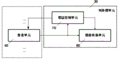
参考图6所示,本发明的技术方案中还提供了一种高动态成像装置,所述高动态成像装置包括图像传感器,具体的还包括:As shown in FIG. 6, a high dynamic imaging device is also provided in the technical solution of the present invention, the high dynamic imaging device includes an image sensor, and specifically includes:
所述图像传感器中的像素阵列,包括多个像素单元40;The pixel array in the image sensor includes a plurality of
列处理单元,包括增益控制单元70和模数转换单元80;A column processing unit, including a
所述像素单元40包括两个具有不同感光灵敏度的光电转换单元;The
所述增益控制单元70,用于根据所述像素单元40输出的信号电压判断图像所处的亮度范围,并根据所述亮度范围调整所述像素单元中进行信号转换的光电转换单元、所述像素单元的电荷-电压转换增益和所述列处理单元的电压增益。The
具体的,所述增益控制单元70包括:Specifically, the
增益档位电压提供单元,适于提供增益档位电压与所述像素单元的输出信号电压进行一次或多次比较,以判断当前图像所处的亮度范围;The gain gear voltage providing unit is adapted to provide a gain gear voltage for one or more comparisons with the output signal voltage of the pixel unit, so as to determine the brightness range of the current image;
增益控制信号产生单元,根据所述图像所处的亮度范围,产生对所述像素单元中光电转换单元选择、转换增益设置和所述列处理单元的电压增益设置的控制信号。The gain control signal generation unit generates control signals for selecting the photoelectric conversion unit in the pixel unit, setting the conversion gain, and setting the voltage gain of the column processing unit according to the brightness range of the image.
结合图6所示,参考图7、图8和图9,其中,图7为一种具体实施方式中的高动态图像传感器中的像素结构的电路图,图8为图7所示的像素结构的读出时序示意图,图9为另一种具体的实施方式中的高动态图像传感器中的像素结构电路图。In combination with FIG. 6 , refer to FIG. 7 , FIG. 8 and FIG. 9 , wherein FIG. 7 is a circuit diagram of a pixel structure in a high dynamic image sensor in a specific embodiment, and FIG. 8 is a circuit diagram of the pixel structure shown in FIG. 7 Schematic diagram of readout sequence, FIG. 9 is a circuit diagram of a pixel structure in a high dynamic image sensor in another specific implementation manner.
图7或图9所示的像素结构中,包括两个具有不同感光灵敏度的光电转换单元,所述光电转换单元分别包括第一光电转换单元PD1和第二光电转换单元PD2。在本实施例中,所述第一光电转换单元PD1的感光灵敏度高于所述第二光电转换单元PD2的感光灵敏度。The pixel structure shown in FIG. 7 or FIG. 9 includes two photoelectric conversion units with different photosensitivity, and the photoelectric conversion units respectively include a first photoelectric conversion unit PD1 and a second photoelectric conversion unit PD2 . In this embodiment, the photosensitivity of the first photoelectric conversion unit PD1 is higher than the photosensitivity of the second photoelectric conversion unit PD2.
本实施例中,所述光电转换单元分别包括光电转换部和传输栅极,所述像素单元还包括浮置扩散区FD,所述传输栅极适于将所述光电转换部中的电荷传输至所述浮置扩散区FD。在本实施例中,所述传输栅极为传输晶体管TXL和TXS。In this embodiment, the photoelectric conversion unit includes a photoelectric conversion part and a transfer gate, and the pixel unit further includes a floating diffusion region FD, and the transfer gate is adapted to transfer the charge in the photoelectric conversion part to The floating diffusion FD. In this embodiment, the transfer gates are transfer transistors TXL and TXS.
在本实施例中,所述第一光电转换单元和所述第二光电转换单元之间设置有第一开关单元DCG,所述第一开关单元DCG适于切换不同的所述光电转换单元连通列处理单元。In this embodiment, a first switch unit DCG is arranged between the first photoelectric conversion unit and the second photoelectric conversion unit, and the first switch unit DCG is adapted to switch between different connected columns of the photoelectric conversion units. processing unit.
所述光电转换单元和所述浮置扩散区FD设置在第一参考电压Vref1和第二参考电压Vref2之间,所述浮置扩散区FD与所述第一参考电压Vref1之间设置有第一参考电压选通晶体管,所述浮置扩散区FD与所述第二参考电压Vref2之间设置有复位晶体管RST。The photoelectric conversion unit and the floating diffusion region FD are disposed between a first reference voltage Vref1 and a second reference voltage Vref2, and a first voltage is disposed between the floating diffusion region FD and the first reference voltage Vref1. A reference voltage gates the transistor, and a reset transistor RST is provided between the floating diffusion region FD and the second reference voltage Vref2.
所述第一光电转换单元PD1连接第一参考电压选通晶体管的栅极,所述第一参考电压选通晶体管的源漏极分别连接所述第一参考电压Vref1,和所述列选通晶体管SEL,所述SEL列选通晶体管的栅极连接列选通信号。The first photoelectric conversion unit PD1 is connected to the gate of a first reference voltage gate transistor, the source and drain of the first reference voltage gate transistor are respectively connected to the first reference voltage Vref1, and the column gate transistor SEL, the gate of the SEL column selection transistor is connected to a column selection signal.
所述第二光电转换单元PD2朝向所述浮置扩散区FD的一端设置有浮动电荷存储区CF,所述浮动电荷存储区CF远离所述第二光电转换单元PD2的一端连接电源电压VSSC,所述浮动电荷存储区CF适于存储在曝光过程中由第二光电转换单元PD2溢出的电子,并在被接入时提供不同的转换增益。本实施例中,所述浮动电荷存储区CF为电容。The end of the second photoelectric conversion unit PD2 facing the floating diffusion region FD is provided with a floating charge storage area CF, and the end of the floating charge storage area CF away from the second photoelectric conversion unit PD2 is connected to the power supply voltage VSSC, so The floating charge storage area CF is suitable for storing electrons overflowed by the second photoelectric conversion unit PD2 during the exposure process, and provides different conversion gains when switched on. In this embodiment, the floating charge storage area CF is a capacitor.
根据所述浮动电荷存储区CF的电容结构,所述电源电压VSSC可以为高电平、低电平、或者变化的波形电压。According to the capacitance structure of the floating charge storage area CF, the power supply voltage VSSC can be a high level, a low level, or a variable waveform voltage.
所述浮动电荷存储区域所述第二光电转换单元之间还设置有浮动电荷导通晶体管TGC,适于在需要时导通所述浮动电荷存储区CF。A floating charge conduction transistor TGC is further arranged between the floating charge storage region and the second photoelectric conversion unit, adapted to turn on the floating charge storage region CF when needed.
本实施例中,在感光灵敏度较低的第二光电转换单元PD2的浮置扩散区域FD引入的浮动电荷导通晶体管TGC和浮动电荷存储区(电容)CF可以实现对极高亮度下PD2曝光过程中溢出电荷的积累,进一步提升动态范围。In this embodiment, the floating charge conduction transistor TGC and the floating charge storage area (capacitor) CF introduced in the floating diffusion area FD of the second photoelectric conversion unit PD2 with low photosensitivity can realize the exposure process of PD2 under extremely high brightness. The accumulation of overflow charges further improves the dynamic range.
参考图7所示,所述浮动电荷存储区(CF)和所述浮置扩散区之间设置有第二开关晶体管TGS。Referring to FIG. 7 , a second switching transistor TGS is disposed between the floating charge storage area (CF) and the floating diffusion area.
参考图9所示,其中所述浮动电荷存储区域所述第二光电转换单元之间还设置有与所述浮动电荷导通晶体管TGC并联的第四开关单元RGC,以控制曝光时间对所述浮动电荷存储区的接入。所述第一开关单元DCG和所述第二光电转换单元之间还设置有第五开关单元TGX。Referring to FIG. 9 , a fourth switching unit RGC connected in parallel with the floating charge conduction transistor TGC is arranged between the floating charge storage region and the second photoelectric conversion unit to control the exposure time for the floating charge. Access to the charge storage area. A fifth switch unit TGX is further arranged between the first switch unit DCG and the second photoelectric conversion unit.
本实施例中,所述第一光电转换单元包括第一传输栅极TX1和第一光电转换单元PD1。In this embodiment, the first photoelectric conversion unit includes a first transfer gate TX1 and a first photoelectric conversion unit PD1.
所述第二光电转换单元包括第二传输栅极TX2和第二光电转换单元PD2。The second photoelectric conversion unit includes a second transfer gate TX2 and a second photoelectric conversion unit PD2.
在以上实施例中,两次预判断中各提供一个参考电压,根据判断结果决定DCG和TGC的开关,两个PD的读出过程较为独立,需要进行两次信号电压的读出。In the above embodiment, a reference voltage is provided in each of the two pre-judgments, and the switches of DCG and TGC are determined according to the judgment results. The readout process of the two PDs is relatively independent, and two signal voltage readouts are required.
参考图11,为其读出时序。在图11所示的读出时序的过程之前,还包括:Referring to Fig. 11, it reads out the sequence. Before the process of reading the sequence shown in Figure 11, it also includes:
清空当前行各所述像素单元的光电转换单元PD1和PD2;Empty the photoelectric conversion units PD1 and PD2 of each pixel unit in the current row;
对当前行各所述光电转换单元PD1和PD2上的光生载流子进行积分;Integrating the photogenerated carriers on each of the photoelectric conversion units PD1 and PD2 in the current row;
对当前行各所述像素单元40的浮置扩散区FD进行复位;Resetting the floating diffusion FD of each
设置当前行各所述像素单元的电荷-电压转换增益档位;Setting the charge-voltage conversion gain gear of each pixel unit in the current row;
设置图像传感器的列信号处理单元的电压增益档位;Setting the voltage gain gear of the column signal processing unit of the image sensor;
具体的,在图11所示的读出时序的详细过程如下:Specifically, the detailed process of the read sequence shown in FIG. 11 is as follows:
1)设置DCG信号为高,DCG管开启,读出FD结点参考电压R1L(Reference/PD1/LowCG);1) Set the DCG signal to high, turn on the DCG tube, and read out the FD node reference voltage R1L (Reference/PD1/LowCG);
2)DCG信号为低,DCG管关断,读出FD结点参考电压R1H(Reference/PD1/High CG)2) The DCG signal is low, the DCG tube is turned off, and the FD node reference voltage R1H (Reference/PD1/High CG) is read out
通过阶段1)和2)转换并保存浮置扩散区在特定档位设置状态下的转换参考值参考电压R1L和参考电压R1H;Through stages 1) and 2), convert and save the conversion reference value reference voltage R1L and reference voltage R1H of the floating diffusion area in a specific gear setting state;
3)将当前行各所述像素单元的转移晶体管TX1管开启,在曝光过程中积累在PD1中的电子转移到FD上;3) Turn on the transfer transistor TX1 of each pixel unit in the current row, and transfer the electrons accumulated in PD1 to FD during the exposure process;
各列信号处理单元检测该列对应的像素单元的浮置扩散区的信号电压FD结点电压,进行第一次预判段,并相应地设置该列对应的像素单元的电荷-电压转换增益档位,具体的:Each column signal processing unit detects the signal voltage FD node voltage of the floating diffusion area of the pixel unit corresponding to the column, performs the first pre-judgment stage, and sets the charge-voltage conversion gain level of the pixel unit corresponding to the column accordingly bits, specifically:
若PXD<Vref1,则判断当前亮度较高,令DCG=1,反之则判断当前处于较低亮度,令DCG=0;If PXD<Vref1, it is judged that the current brightness is high, and DCG=1; otherwise, it is judged that the current brightness is low, and DCG=0;
4)根据阶段3)的判断结果,各列信号处理单元同时转换对应像素单元的浮置扩散区的信号电压,得到当前行的转换信号值。具体地,控制DCG管开启或关断,再令TX1开启一次,然后读出FD结点的信号电压S1(Signal/PD1);4) According to the judgment result of stage 3), the signal processing units of each column simultaneously convert the signal voltage of the floating diffusion area of the corresponding pixel unit to obtain the converted signal value of the current row. Specifically, control the DCG tube to turn on or off, and then turn on TX1 once, and then read the signal voltage S1 (Signal/PD1) of the FD node;
5)使DCG管和TGS管保持开启,短暂开启RST管,读出FD结点参考电压R2H(Reference/PD2/High CG)TX2管开启,在曝光过程中积累在PD2中的电子转移到FD上,读出FD结点电压,进行第二次预判段,若PXD<Vref2,则处于极亮亮度,令TGC=1,反之则令TGC=0;5) Keep the DCG tube and TGS tube turned on, turn on the RST tube briefly, read the FD node reference voltage R2H (Reference/PD2/High CG) TX2 tube is turned on, and the electrons accumulated in PD2 are transferred to FD during the exposure process , read out the FD node voltage, and carry out the second pre-judgment stage, if PXD<Vref2, it is in extremely bright brightness, set TGC=1, otherwise, set TGC=0;
6)根据阶段6)的判断结果,控制TGC管开启或关断,再令TX2开启一次,然后读出FD结点的信号电压S2(Signal/PD2);6) According to the judgment result of stage 6), control the TGC tube to turn on or off, and then turn on TX2 once, and then read the signal voltage S2 (Signal/PD2) of the FD node;
7)使TGC管保持开启,短暂开启RST管,读出FD结点参考电压R2L(Reference/PD2/Low CG);7) Keep the TGC tube turned on, turn on the RST tube briefly, and read the reference voltage R2L (Reference/PD2/Low CG) of the FD node;
说明:Vref1和Vref2可以相同,也可以不同。Note: Vref1 and Vref2 can be the same or different.
图10所示为本发明所提供的技术方案中一种实施例的图像处理系统。包括:FIG. 10 shows an image processing system of an embodiment of the technical solution provided by the present invention. include:
如上所述的高动态成像装置50;A high
行驱动单元30;
同一行的所述像素单元40连接到同一行控制线LL,所述行驱动单元30通过所述行控制线LL对像素单元进行驱动和控制;The
同一列像素单元连接到同一列信号线CL,所述像素单元的输出信号经由所述列信号线CL输出到列处理单元20。Pixel units in the same column are connected to the same column signal line CL, and output signals of the pixel units are output to the
同一列像素单元连接到同一列控制线CC,所述列处理单元通过所述列控制线对像素单元进行驱动和控制。Pixel units in the same column are connected to the same column control line CC, and the column processing unit drives and controls the pixel unit through the column control line.
进一步的,参考图11所示,本发明所提供的技术方案中另一种实施例的图像处理系统,还包括列存储单元10,所述列处理单元20将对所述像素单元输出信号的模数结果存储所述到列存储单元10。Further, as shown in FIG. 11 , the image processing system of another embodiment of the technical solution provided by the present invention further includes a
本发明的技术方案所提供的图像处理系统中,列处理单元在检测出图像亮度区间后,增益控制单元在调整像素单元输出信号的模拟增益的基础上,同时可以切换像素单元的转换增益,尤其是对于有多个光电二极管的像素结构,在光电二极管的选择上也可以自适应的切换,减少读取数据的次数和时间,降低对数据处理和存储的需求,提高帧率。In the image processing system provided by the technical solution of the present invention, after the column processing unit detects the brightness interval of the image, the gain control unit can switch the conversion gain of the pixel unit on the basis of adjusting the analog gain of the output signal of the pixel unit, especially For a pixel structure with multiple photodiodes, the selection of photodiodes can also be adaptively switched, reducing the number and time of reading data, reducing the demand for data processing and storage, and increasing the frame rate.
本发明虽然已以较佳实施例公开如上,但其并不是用来限定本发明,任何本领域技术人员在不脱离本发明的精神和范围内,都可以利用上述揭示的方法和技术内容对本发明技术方案做出可能的变动和修改,因此,凡是未脱离本发明技术方案的内容,依据本发明的技术实质对以上实施例所作的任何简单修改、等同变化及修饰,均属于本发明技术方案的保护范围。Although the present invention has been disclosed as above with preferred embodiments, it is not intended to limit the present invention, and any person skilled in the art can use the methods disclosed above and technical content to analyze the present invention without departing from the spirit and scope of the present invention. Possible changes and modifications are made in the technical solution. Therefore, any simple modification, equivalent change and modification made to the above embodiments according to the technical essence of the present invention, which do not depart from the content of the technical solution of the present invention, all belong to the technical solution of the present invention. protected range.
Claims (21)
Priority Applications (3)
| Application Number | Priority Date | Filing Date | Title |
|---|---|---|---|
| CN202111657558.3A CN116419082A (en) | 2021-12-31 | 2021-12-31 | Realization method of high dynamic imaging and its device, image processing system |
| PCT/CN2022/123969 WO2023124355A1 (en) | 2021-12-31 | 2022-10-09 | Method and device for implementing high-dynamic range imaging, and image processing system |
| US18/864,408 US20250247635A1 (en) | 2021-12-31 | 2022-10-09 | Method and device for implementing high-dynamic range imaging, and image processing system |
Applications Claiming Priority (1)
| Application Number | Priority Date | Filing Date | Title |
|---|---|---|---|
| CN202111657558.3A CN116419082A (en) | 2021-12-31 | 2021-12-31 | Realization method of high dynamic imaging and its device, image processing system |
Publications (1)
| Publication Number | Publication Date |
|---|---|
| CN116419082A true CN116419082A (en) | 2023-07-11 |
Family
ID=86997441
Family Applications (1)
| Application Number | Title | Priority Date | Filing Date |
|---|---|---|---|
| CN202111657558.3A Pending CN116419082A (en) | 2021-12-31 | 2021-12-31 | Realization method of high dynamic imaging and its device, image processing system |
Country Status (3)
| Country | Link |
|---|---|
| US (1) | US20250247635A1 (en) |
| CN (1) | CN116419082A (en) |
| WO (1) | WO2023124355A1 (en) |
Cited By (1)
| Publication number | Priority date | Publication date | Assignee | Title |
|---|---|---|---|---|
| CN117336623A (en) * | 2023-11-24 | 2024-01-02 | 上海芯歌智能科技有限公司 | Machine vision measurement system and sensor chip simulation parameter adjustment method |
Families Citing this family (1)
| Publication number | Priority date | Publication date | Assignee | Title |
|---|---|---|---|---|
| TW202425302A (en) * | 2022-08-22 | 2024-06-16 | 日商索尼半導體解決方案公司 | Solid-state imaging device |
Citations (5)
| Publication number | Priority date | Publication date | Assignee | Title |
|---|---|---|---|---|
| US20150054973A1 (en) * | 2013-08-23 | 2015-02-26 | Aptina Imaging Corporation | Imaging systems and methods for performing column-based image sensor pixel gain adjustments |
| US20150350574A1 (en) * | 2014-05-27 | 2015-12-03 | Canon Kabushiki Kaisha | Image sensor and control method thereof, and image capturing apparatus |
| CN108419032A (en) * | 2018-03-01 | 2018-08-17 | 上海晔芯电子科技有限公司 | HDR image sensor pixel structure and imaging system supporting multiple exposure modes |
| US20210144319A1 (en) * | 2019-11-08 | 2021-05-13 | Semiconductor Components Industries, Llc | Systems and methods for generating high dynamic range images |
| CN113206963A (en) * | 2020-01-30 | 2021-08-03 | 半导体元件工业有限责任公司 | High dynamic range imaging pixel with multiple photodiodes |
Family Cites Families (4)
| Publication number | Priority date | Publication date | Assignee | Title |
|---|---|---|---|---|
| CN104580945B (en) * | 2014-12-29 | 2018-08-10 | 上海集成电路研发中心有限公司 | A kind of image sensor architecture and method for realizing high dynamic range images |
| US9854186B2 (en) * | 2016-02-05 | 2017-12-26 | Semiconductor Components Industries, Llc | Methods and apparatus for an images sensor with row-level gain control |
| CN109951655B (en) * | 2017-12-21 | 2022-02-25 | 格科微电子(上海)有限公司 | Method for realizing double conversion gain image sensor |
| CN111294529B (en) * | 2020-03-11 | 2021-11-16 | 长春长光辰芯光电技术有限公司 | High dynamic range TDI image sensor and imaging method thereof |
-
2021
- 2021-12-31 CN CN202111657558.3A patent/CN116419082A/en active Pending
-
2022
- 2022-10-09 WO PCT/CN2022/123969 patent/WO2023124355A1/en not_active Ceased
- 2022-10-09 US US18/864,408 patent/US20250247635A1/en active Pending
Patent Citations (5)
| Publication number | Priority date | Publication date | Assignee | Title |
|---|---|---|---|---|
| US20150054973A1 (en) * | 2013-08-23 | 2015-02-26 | Aptina Imaging Corporation | Imaging systems and methods for performing column-based image sensor pixel gain adjustments |
| US20150350574A1 (en) * | 2014-05-27 | 2015-12-03 | Canon Kabushiki Kaisha | Image sensor and control method thereof, and image capturing apparatus |
| CN108419032A (en) * | 2018-03-01 | 2018-08-17 | 上海晔芯电子科技有限公司 | HDR image sensor pixel structure and imaging system supporting multiple exposure modes |
| US20210144319A1 (en) * | 2019-11-08 | 2021-05-13 | Semiconductor Components Industries, Llc | Systems and methods for generating high dynamic range images |
| CN113206963A (en) * | 2020-01-30 | 2021-08-03 | 半导体元件工业有限责任公司 | High dynamic range imaging pixel with multiple photodiodes |
Cited By (3)
| Publication number | Priority date | Publication date | Assignee | Title |
|---|---|---|---|---|
| CN117336623A (en) * | 2023-11-24 | 2024-01-02 | 上海芯歌智能科技有限公司 | Machine vision measurement system and sensor chip simulation parameter adjustment method |
| CN117336623B (en) * | 2023-11-24 | 2024-02-20 | 上海芯歌智能科技有限公司 | Machine vision measurement system and sensor chip simulation parameter adjustment method |
| WO2025107471A1 (en) * | 2023-11-24 | 2025-05-30 | 上海芯歌智能科技有限公司 | Machine vision measurement system and method for adjusting simulation parameters of sensor chip |
Also Published As
| Publication number | Publication date |
|---|---|
| US20250247635A1 (en) | 2025-07-31 |
| WO2023124355A1 (en) | 2023-07-06 |
Similar Documents
| Publication | Publication Date | Title |
|---|---|---|
| CN103402059B (en) | Imaging device | |
| US8619170B2 (en) | Solid-state image pickup device with plural transfer structures to transfer charge to plural accumulation portions | |
| US9088726B2 (en) | Solid-state image capturing device, method of driving solid-state image capturing device, and image capturing apparatus | |
| US8059173B2 (en) | Correlated double sampling pixel and method | |
| US9826185B2 (en) | High signal to noise ratio of image based on signals with different sensitivities | |
| CN109819184A (en) | Image sensor and method for reducing fixed image noise of image sensor | |
| KR102690091B1 (en) | Solid-state image pickup device and driving method therefor, and electronic apparatus | |
| US9137432B2 (en) | Backside illumination image sensor, operating method thereof, image processing system and method of processing image using the same | |
| EP4344243B1 (en) | Image sensor comprising pixels usable in both rolling shutter and global shutter mode and image processing device including the same | |
| CN108200366A (en) | Pixel unit and the formation method of pixel unit and digital camera imaging system | |
| CN103905748A (en) | Three-dimensional architecture ultra-high-definition CMOS image sensor pixel circuit and its control method | |
| WO2023124355A1 (en) | Method and device for implementing high-dynamic range imaging, and image processing system | |
| KR102519712B1 (en) | Image sensor | |
| US12593125B2 (en) | Image sensor supporting AF function and method of operating the same | |
| CN112670308B (en) | Pixel unit | |
| KR102743552B1 (en) | Image Sensing Device | |
| KR20090117230A (en) | Pixel Circuit and Driving Method of Solid State Imaging Device | |
| JP2012244379A (en) | Solid state image pickup device | |
| CN111314636B (en) | CMOS image sensor with improved column data shift reading | |
| CN120711305A (en) | Pixel signal reading method and device | |
| KR20250154103A (en) | Image Sensor and operating method of image sensor | |
| CN119605160A (en) | Photon counting pixel and method of operation thereof | |
| CN114363537A (en) | Pixel structure and array, circuit and method, image sensor, and storage medium | |
| HK1180863B (en) | Multilevel reset voltage for multi-conversion gain image sensor | |
| HK1180863A1 (en) | Multilevel reset voltage for multi-conversion gain image sensor |
Legal Events
| Date | Code | Title | Description |
|---|---|---|---|
| PB01 | Publication | ||
| PB01 | Publication | ||
| SE01 | Entry into force of request for substantive examination | ||
| SE01 | Entry into force of request for substantive examination |