CN1175461C - Flat display screen and manufacturing method thereof - Google Patents
Flat display screen and manufacturing method thereof Download PDFInfo
- Publication number
- CN1175461C CN1175461C CNB988006847A CN98800684A CN1175461C CN 1175461 C CN1175461 C CN 1175461C CN B988006847 A CNB988006847 A CN B988006847A CN 98800684 A CN98800684 A CN 98800684A CN 1175461 C CN1175461 C CN 1175461C
- Authority
- CN
- China
- Prior art keywords
- display
- electrode
- mentioned
- common electrode
- discharge
- Prior art date
- Legal status (The legal status is an assumption and is not a legal conclusion. Google has not performed a legal analysis and makes no representation as to the accuracy of the status listed.)
- Expired - Fee Related
Links
Images










Classifications
-
- G—PHYSICS
- G09—EDUCATION; CRYPTOGRAPHY; DISPLAY; ADVERTISING; SEALS
- G09G—ARRANGEMENTS OR CIRCUITS FOR CONTROL OF INDICATING DEVICES USING STATIC MEANS TO PRESENT VARIABLE INFORMATION
- G09G3/00—Control arrangements or circuits, of interest only in connection with visual indicators other than cathode-ray tubes
- G09G3/20—Control arrangements or circuits, of interest only in connection with visual indicators other than cathode-ray tubes for presentation of an assembly of a number of characters, e.g. a page, by composing the assembly by combination of individual elements arranged in a matrix no fixed position being assigned to or needed to be assigned to the individual characters or partial characters
- G09G3/22—Control arrangements or circuits, of interest only in connection with visual indicators other than cathode-ray tubes for presentation of an assembly of a number of characters, e.g. a page, by composing the assembly by combination of individual elements arranged in a matrix no fixed position being assigned to or needed to be assigned to the individual characters or partial characters using controlled light sources
- G09G3/28—Control arrangements or circuits, of interest only in connection with visual indicators other than cathode-ray tubes for presentation of an assembly of a number of characters, e.g. a page, by composing the assembly by combination of individual elements arranged in a matrix no fixed position being assigned to or needed to be assigned to the individual characters or partial characters using controlled light sources using luminous gas-discharge panels, e.g. plasma panels
- G09G3/2803—Display of gradations
-
- G—PHYSICS
- G09—EDUCATION; CRYPTOGRAPHY; DISPLAY; ADVERTISING; SEALS
- G09G—ARRANGEMENTS OR CIRCUITS FOR CONTROL OF INDICATING DEVICES USING STATIC MEANS TO PRESENT VARIABLE INFORMATION
- G09G3/00—Control arrangements or circuits, of interest only in connection with visual indicators other than cathode-ray tubes
- G09G3/20—Control arrangements or circuits, of interest only in connection with visual indicators other than cathode-ray tubes for presentation of an assembly of a number of characters, e.g. a page, by composing the assembly by combination of individual elements arranged in a matrix no fixed position being assigned to or needed to be assigned to the individual characters or partial characters
- G09G3/22—Control arrangements or circuits, of interest only in connection with visual indicators other than cathode-ray tubes for presentation of an assembly of a number of characters, e.g. a page, by composing the assembly by combination of individual elements arranged in a matrix no fixed position being assigned to or needed to be assigned to the individual characters or partial characters using controlled light sources
- G09G3/28—Control arrangements or circuits, of interest only in connection with visual indicators other than cathode-ray tubes for presentation of an assembly of a number of characters, e.g. a page, by composing the assembly by combination of individual elements arranged in a matrix no fixed position being assigned to or needed to be assigned to the individual characters or partial characters using controlled light sources using luminous gas-discharge panels, e.g. plasma panels
- G09G3/282—Control arrangements or circuits, of interest only in connection with visual indicators other than cathode-ray tubes for presentation of an assembly of a number of characters, e.g. a page, by composing the assembly by combination of individual elements arranged in a matrix no fixed position being assigned to or needed to be assigned to the individual characters or partial characters using controlled light sources using luminous gas-discharge panels, e.g. plasma panels using DC panels
-
- G—PHYSICS
- G09—EDUCATION; CRYPTOGRAPHY; DISPLAY; ADVERTISING; SEALS
- G09G—ARRANGEMENTS OR CIRCUITS FOR CONTROL OF INDICATING DEVICES USING STATIC MEANS TO PRESENT VARIABLE INFORMATION
- G09G3/00—Control arrangements or circuits, of interest only in connection with visual indicators other than cathode-ray tubes
- G09G3/20—Control arrangements or circuits, of interest only in connection with visual indicators other than cathode-ray tubes for presentation of an assembly of a number of characters, e.g. a page, by composing the assembly by combination of individual elements arranged in a matrix no fixed position being assigned to or needed to be assigned to the individual characters or partial characters
- G09G3/22—Control arrangements or circuits, of interest only in connection with visual indicators other than cathode-ray tubes for presentation of an assembly of a number of characters, e.g. a page, by composing the assembly by combination of individual elements arranged in a matrix no fixed position being assigned to or needed to be assigned to the individual characters or partial characters using controlled light sources
- G09G3/28—Control arrangements or circuits, of interest only in connection with visual indicators other than cathode-ray tubes for presentation of an assembly of a number of characters, e.g. a page, by composing the assembly by combination of individual elements arranged in a matrix no fixed position being assigned to or needed to be assigned to the individual characters or partial characters using controlled light sources using luminous gas-discharge panels, e.g. plasma panels
- G09G3/288—Control arrangements or circuits, of interest only in connection with visual indicators other than cathode-ray tubes for presentation of an assembly of a number of characters, e.g. a page, by composing the assembly by combination of individual elements arranged in a matrix no fixed position being assigned to or needed to be assigned to the individual characters or partial characters using controlled light sources using luminous gas-discharge panels, e.g. plasma panels using AC panels
- G09G3/298—Control arrangements or circuits, of interest only in connection with visual indicators other than cathode-ray tubes for presentation of an assembly of a number of characters, e.g. a page, by composing the assembly by combination of individual elements arranged in a matrix no fixed position being assigned to or needed to be assigned to the individual characters or partial characters using controlled light sources using luminous gas-discharge panels, e.g. plasma panels using AC panels using surface discharge panels
- G09G3/2983—Control arrangements or circuits, of interest only in connection with visual indicators other than cathode-ray tubes for presentation of an assembly of a number of characters, e.g. a page, by composing the assembly by combination of individual elements arranged in a matrix no fixed position being assigned to or needed to be assigned to the individual characters or partial characters using controlled light sources using luminous gas-discharge panels, e.g. plasma panels using AC panels using surface discharge panels using non-standard pixel electrode arrangements
-
- H—ELECTRICITY
- H01—ELECTRIC ELEMENTS
- H01J—ELECTRIC DISCHARGE TUBES OR DISCHARGE LAMPS
- H01J11/00—Gas-filled discharge tubes with alternating current induction of the discharge, e.g. alternating current plasma display panels [AC-PDP]; Gas-filled discharge tubes without any main electrode inside the vessel; Gas-filled discharge tubes with at least one main electrode outside the vessel
- H01J11/10—AC-PDPs with at least one main electrode being out of contact with the plasma
- H01J11/12—AC-PDPs with at least one main electrode being out of contact with the plasma with main electrodes provided on both sides of the discharge space
-
- H—ELECTRICITY
- H01—ELECTRIC ELEMENTS
- H01J—ELECTRIC DISCHARGE TUBES OR DISCHARGE LAMPS
- H01J11/00—Gas-filled discharge tubes with alternating current induction of the discharge, e.g. alternating current plasma display panels [AC-PDP]; Gas-filled discharge tubes without any main electrode inside the vessel; Gas-filled discharge tubes with at least one main electrode outside the vessel
- H01J11/20—Constructional details
- H01J11/22—Electrodes, e.g. special shape, material or configuration
-
- H—ELECTRICITY
- H01—ELECTRIC ELEMENTS
- H01J—ELECTRIC DISCHARGE TUBES OR DISCHARGE LAMPS
- H01J11/00—Gas-filled discharge tubes with alternating current induction of the discharge, e.g. alternating current plasma display panels [AC-PDP]; Gas-filled discharge tubes without any main electrode inside the vessel; Gas-filled discharge tubes with at least one main electrode outside the vessel
- H01J11/20—Constructional details
- H01J11/34—Vessels, containers or parts thereof, e.g. substrates
-
- H—ELECTRICITY
- H01—ELECTRIC ELEMENTS
- H01J—ELECTRIC DISCHARGE TUBES OR DISCHARGE LAMPS
- H01J9/00—Apparatus or processes specially adapted for the manufacture, installation, removal, maintenance of electric discharge tubes, discharge lamps, or parts thereof; Recovery of material from discharge tubes or lamps
- H01J9/24—Manufacture or joining of vessels, leading-in conductors or bases
- H01J9/241—Manufacture or joining of vessels, leading-in conductors or bases the vessel being for a flat panel display
-
- G—PHYSICS
- G09—EDUCATION; CRYPTOGRAPHY; DISPLAY; ADVERTISING; SEALS
- G09G—ARRANGEMENTS OR CIRCUITS FOR CONTROL OF INDICATING DEVICES USING STATIC MEANS TO PRESENT VARIABLE INFORMATION
- G09G2300/00—Aspects of the constitution of display devices
- G09G2300/02—Composition of display devices
- G09G2300/026—Video wall, i.e. juxtaposition of a plurality of screens to create a display screen of bigger dimensions
-
- G—PHYSICS
- G09—EDUCATION; CRYPTOGRAPHY; DISPLAY; ADVERTISING; SEALS
- G09G—ARRANGEMENTS OR CIRCUITS FOR CONTROL OF INDICATING DEVICES USING STATIC MEANS TO PRESENT VARIABLE INFORMATION
- G09G2320/00—Control of display operating conditions
- G09G2320/02—Improving the quality of display appearance
- G09G2320/0285—Improving the quality of display appearance using tables for spatial correction of display data
-
- G—PHYSICS
- G09—EDUCATION; CRYPTOGRAPHY; DISPLAY; ADVERTISING; SEALS
- G09G—ARRANGEMENTS OR CIRCUITS FOR CONTROL OF INDICATING DEVICES USING STATIC MEANS TO PRESENT VARIABLE INFORMATION
- G09G3/00—Control arrangements or circuits, of interest only in connection with visual indicators other than cathode-ray tubes
- G09G3/20—Control arrangements or circuits, of interest only in connection with visual indicators other than cathode-ray tubes for presentation of an assembly of a number of characters, e.g. a page, by composing the assembly by combination of individual elements arranged in a matrix no fixed position being assigned to or needed to be assigned to the individual characters or partial characters
- G09G3/2007—Display of intermediate tones
- G09G3/2018—Display of intermediate tones by time modulation using two or more time intervals
-
- G—PHYSICS
- G09—EDUCATION; CRYPTOGRAPHY; DISPLAY; ADVERTISING; SEALS
- G09G—ARRANGEMENTS OR CIRCUITS FOR CONTROL OF INDICATING DEVICES USING STATIC MEANS TO PRESENT VARIABLE INFORMATION
- G09G3/00—Control arrangements or circuits, of interest only in connection with visual indicators other than cathode-ray tubes
- G09G3/20—Control arrangements or circuits, of interest only in connection with visual indicators other than cathode-ray tubes for presentation of an assembly of a number of characters, e.g. a page, by composing the assembly by combination of individual elements arranged in a matrix no fixed position being assigned to or needed to be assigned to the individual characters or partial characters
- G09G3/22—Control arrangements or circuits, of interest only in connection with visual indicators other than cathode-ray tubes for presentation of an assembly of a number of characters, e.g. a page, by composing the assembly by combination of individual elements arranged in a matrix no fixed position being assigned to or needed to be assigned to the individual characters or partial characters using controlled light sources
- G09G3/28—Control arrangements or circuits, of interest only in connection with visual indicators other than cathode-ray tubes for presentation of an assembly of a number of characters, e.g. a page, by composing the assembly by combination of individual elements arranged in a matrix no fixed position being assigned to or needed to be assigned to the individual characters or partial characters using controlled light sources using luminous gas-discharge panels, e.g. plasma panels
- G09G3/288—Control arrangements or circuits, of interest only in connection with visual indicators other than cathode-ray tubes for presentation of an assembly of a number of characters, e.g. a page, by composing the assembly by combination of individual elements arranged in a matrix no fixed position being assigned to or needed to be assigned to the individual characters or partial characters using controlled light sources using luminous gas-discharge panels, e.g. plasma panels using AC panels
- G09G3/296—Driving circuits for producing the waveforms applied to the driving electrodes
Landscapes
- Engineering & Computer Science (AREA)
- Physics & Mathematics (AREA)
- Plasma & Fusion (AREA)
- Computer Hardware Design (AREA)
- General Physics & Mathematics (AREA)
- Theoretical Computer Science (AREA)
- Chemical & Material Sciences (AREA)
- Materials Engineering (AREA)
- Power Engineering (AREA)
- Manufacturing & Machinery (AREA)
- Gas-Filled Discharge Tubes (AREA)
- Control Of Indicators Other Than Cathode Ray Tubes (AREA)
- Control Of Gas Discharge Display Tubes (AREA)
- Manufacture Of Electron Tubes, Discharge Lamp Vessels, Lead-In Wires, And The Like (AREA)
- Devices For Indicating Variable Information By Combining Individual Elements (AREA)
Abstract
Description
技术领域technical field
本发明涉及显示字符、图形、图象等的平面型的显示屏即平面显示屏及其制造方法、以及其控制装置和其驱动方法。The present invention relates to a flat display screen for displaying characters, graphics, images, etc., that is, a flat display screen, a manufacturing method thereof, a control device thereof, and a driving method thereof.
背景技术Background technique
迄今,作为平面显示屏是这样来构成的,即将夹住能放电的气体媒体并列设置的多条线状电极配置成矩阵状,将电压加在所选择的两电极之间,由此在两电极的交点处引起气体放电,这样的平面显示屏例如有日本国特开平3-160488号公报、特开平2-90192号公报及实开平3-94751号公报所示的平面显示屏。So far, as a flat display screen, it has been constructed in such a way that a plurality of linear electrodes arranged side by side between a dischargeable gas medium are arranged in a matrix, and a voltage is applied between the selected two electrodes, thereby creating a positive voltage between the two electrodes. A gas discharge is caused at the intersection of the two. Such flat display screens include, for example, the flat display screens shown in Japanese Patent Application Laid-Open No. 3-160488, Japanese Patent Laid-Open No. 2-90192 and Japanese Patent Laid-Open No. 3-94751.
可是,上述现有例的平面显示屏是将具有透光性的两片绝缘基板粘贴起来形成空间,将电极分别设置在各基板上,隔开一定空间相对地配置,以便在空间内形成矩阵状的放电用电极,同时将区分放电空间用的隔壁设置在每个电极上,由于这样来构成,所以通过选择呈矩阵状相对地配置的电极进行显示控制,而不能对各个显示单元独立地进行显示控制。另外,由于如上构成,所以显示屏的平面厚度不得不做得厚些。However, in the flat panel display of the above conventional example, two light-transmitting insulating substrates are pasted together to form a space, and the electrodes are respectively arranged on each substrate, and are arranged opposite to each other with a certain space apart, so as to form a matrix in the space. Each electrode is provided with a partition wall for distinguishing the discharge space. Due to this structure, display control is performed by selecting electrodes that are arranged opposite to each other in a matrix, and it is not possible to display independently for each display unit. control. In addition, due to the above configuration, the planar thickness of the display screen has to be thicker.
另外,迄今作为利用气体放电进行显示的平面型的屏,有1983年11月发行的由大胁、吉田著的“等离子体显示器”中记载的屏。In addition, conventionally, as a flat panel for displaying by gas discharge, there is a panel described in "Plasma Display" by Owaki and Yoshida, published in November 1983.
该屏是这样来构成的:将用玻璃等绝缘体覆盖的梳形电极配置成呈矩阵状彼此相对而将在放电空间夹在中间,另外,由单一的梳形电极一并地驱动构成行或列的显示单元。The screen is constructed in such a way that the comb-shaped electrodes covered with an insulator such as glass are arranged to face each other in a matrix and sandwich the discharge space. In addition, a single comb-shaped electrode is driven together to form a row or column. display unit.
另外,通过以下三方面的工作进行显示控制:用构成行列的梳形电极依次驱动扫描侧的梳形电极,使所选择的梳形电极和矩阵对置电极之间的显示单元中发生微小放电的写入工作;通过该写入工作,有选择地只使发生了微小放电的显示单元而且使全体显示画面发光的维持工作;以及使全体画面的显示单元的电气状态变得一致用的全面写入、全面消除工作。In addition, the display control is carried out through the following three aspects: the comb-shaped electrodes on the scanning side are sequentially driven by the comb-shaped electrodes constituting the rows and columns, and the micro-discharge occurs in the display unit between the selected comb-shaped electrode and the matrix opposite electrode. Writing operation; through this writing operation, only the display unit in which the micro discharge has occurred is selectively maintained and the entire display screen is illuminated; and the overall writing is used to make the electrical state of the display unit of the entire screen uniform , Comprehensive elimination of work.
另外,为了进行图象显示,需要进行每个显示单元的亮度控制,但控制和显示的电极同时处理多个显示单元,显示单元具有双值工作(只能取发光·不发光两种状态)的特性,由于这种关系,如果不采用特殊的方法就不能进行深淡等级显示,例如采用日本国特开平6-186927号公报中记载的驱动方法。In addition, in order to display images, it is necessary to control the brightness of each display unit, but the electrodes for control and display process multiple display units at the same time, and the display unit has the characteristics of dual-value work (only two states of light-emitting and non-light-emitting) Due to this relationship, the gradation display cannot be performed without a special method, such as the driving method described in Japanese Patent Application Laid-Open No. 6-186927.
它是这样一种方式:为了表现亮度,将显示期间分成维持期间不同(维持期间的亮度不同)的多个期间,在各个期间内通过进行显示数据的写入、维持工作,对各个期间的亮度进行组合,进行深淡等级显示。It is such a method: In order to express the brightness, the display period is divided into multiple periods with different sustain periods (the brightness of the sustain period is different), and the brightness of each period is adjusted by writing and maintaining display data in each period. Combine them to display the shade level.
可是,该现有的屏的驱动方法由于控制对置的矩阵电极进行显示放电,所以这些电极一并控制100个以上的多个显示单元,为了进行显示,必须在时间方面按顺序进行以下工序:用呈矩阵排列的电极组依次对扫描电极进行扫描而进行的写入工序;将维持电压脉冲交替地加在矩阵电极组上,只使进行写入的显示单元进行发光显示的维持工序;使显示单元、非显示单元的电气状态变得一致而进行的全面放电、全面消除工序。But, because the driving method of this existing screen controls opposite matrix electrodes to carry out display discharge, so these electrodes control a plurality of display units more than 100 together, in order to display, must carry out the following steps in order in terms of time: The writing process of scanning the scanning electrodes sequentially with electrode groups arranged in a matrix; the sustaining process of applying sustain voltage pulses alternately to the matrix electrode groups to make only the display unit to be written perform light-emitting display; to make the display The process of fully discharging and completely erasing the electrical state of the unit and non-display unit becomes the same.
另外,在这样的时序控制中,控制过程必定在很大程度上依赖于下述的显示单元的特性、即各个显示单元的放电开始电压值、维持放电用的最小电压值、发生写入放电用的写入电压值等,而这些特性容易受到制造工序中的大的个体差别的影响。特别是维持放电用的电压,在高电压侧被放电开始电压所限制,在低电压侧被最小维持电压所限制,所以多半只有10~20V左右的幅度。In addition, in such sequential control, the control process must largely depend on the characteristics of the following display cells, that is, the discharge start voltage value of each display cell, the minimum voltage value for sustain discharge, and the voltage value for generating write discharge. However, these characteristics are easily affected by large individual differences in the manufacturing process. In particular, the voltage for sustain discharge is limited by the discharge start voltage on the high voltage side and by the minimum sustain voltage on the low voltage side, so it is often only in the range of about 10 to 20V.
由于以上的理由,稳定地进行显示用的控制容限不能取得大,需要对显示屏分别调整维持显示用的电压、写入用的电压、放电开始用的电压等,如果这些电压值由于持续工作而变化时,需要再调整。另外,即使在一片显示屏上由于结合得复杂的显示单元的特性变化大,存在产品合格率低的问题。Due to the above reasons, the control margin for stable display cannot be obtained large, and it is necessary to separately adjust the voltage for maintaining display, the voltage for writing, the voltage for starting discharge, etc. for the display screen. If these voltage values are due to continuous operation And when it changes, it needs to be readjusted. In addition, even on one display screen, there is a problem of low product yield due to large variations in the characteristics of the complexly combined display units.
另外,如上所述,在现有的气体放电屏的深淡等级控制方式中,由于需要以能表现深淡等级的足够的次数来进行数据的写入、维持显示这样的至少两种工作,再者,写入工作至少需要1~2毫秒,所以显示的维持期间由于插进了写入期间而变得不连续。In addition, as mentioned above, in the existing gradation level control method of the gas discharge panel, at least two operations such as writing data and maintaining the display need to be performed at least two times to express the gradation level. Or, at least 1 to 2 milliseconds are required for the writing operation, so the display maintenance period becomes discontinuous due to the insertion of the writing period.
作为深淡等级表现,控制成用一个时序(约16毫秒:帧频60Hz)结束,但由于在一个时序内不可能进行在时间上连续的亮度控制,所以产生显示的深淡等级表现(由屏驱动进行的设计方面的深淡等级表现)和人的眼睛产生的对亮度变化的感觉不一致性。因此,还包括能察觉到称为模拟轮廓的深淡等级的不连续点,图象显示的品质降低很多的问题。As a gradation display, the control ends with a sequence (about 16 milliseconds:
发明内容Contents of the invention
本发明就是鉴于上述问题而完成的,其目的在于获得一种能逐个地驱动显示屏的每一个显示单元、而且具有能使平面厚度变薄的放电空间结构的平面显示屏及其制造方法。The present invention has been made in view of the above problems, and its object is to obtain a flat display panel capable of individually driving each display unit of the display panel and having a discharge space structure capable of reducing the planar thickness, and a method of manufacturing the same.
另一个目的在于获得这样一种平面显示屏的控制装置,该装置对于平面显示屏的每个显示单元中的独立的个别电极能逐个地进行开关控制且能进行深淡等级控制,其中能对每一个显示单元逐个进行驱动。Another object is to obtain such a control device for a flat display screen, which can switch and control the individual electrodes in each display unit of the flat display screen one by one and can control the intensity level, wherein each A display unit is driven one by one.
另一个目的在于获得这样一种平面显示屏的驱动方法,该方法对于具有能逐个地驱动每一个显示单元的电极结构、屏结构的屏,能与每个显示单元具有的放电特性、特别是与放电开始电压和最小放电维持电压之差无关地进行维持放电的控制,获得足够大的放电控制的容限,还通过在每一定期间内插入使放电稳定的工作而能维持稳定的放电。Another object is to obtain such a driving method of a flat display screen, which can be compatible with the discharge characteristics that each display unit has, especially with Sustaining the discharge is controlled regardless of the difference between the discharge start voltage and the minimum discharge sustaining voltage, a sufficiently large discharge control margin is obtained, and a stable discharge can be maintained by inserting an operation to stabilize the discharge every predetermined period.
另一个目的在于获得这样一种平面显示屏的驱动方法,该方法通过在一个时序内的连续的时间范围进行放电控制,能在一个集中的期间表现显示亮度、能进行适合于图象显示的深淡等级显示。Another object is to obtain such a driving method of a flat panel display, which can display display brightness in a concentrated period and perform deep display suitable for image display by performing discharge control in a continuous time range within a time sequence. Light level display.
本发明的平面显示屏备有:第一透明基板;设置在上述第一透明基板上的一对电极;以及在与上述一对电极相对的部分设有凹部,并没有电极而形成显示单元的放电空间的第二基板,由此提供一种能逐个地驱动显示屏的每一个显示单元、且具有能使平面厚度变薄的放电空间结构的平面显示屏。The flat display screen of the present invention is equipped with: a first transparent substrate; a pair of electrodes arranged on the above-mentioned first transparent substrate; The second substrate of the space, thereby providing a flat display panel capable of driving each display unit of the display panel one by one and having a discharge space structure capable of making the planar thickness thinner.
另外,在上述第一透明基板上并列设置多对电极以构成电极组,因而容易形成多个显示单元的电极结构。In addition, a plurality of pairs of electrodes are arranged side by side on the above-mentioned first transparent substrate to form an electrode group, so it is easy to form an electrode structure of a plurality of display units.
另外,上述凹部呈矩形且具有所希望的深度,所以不设置区分放电空间用的隔壁、而且能在与电极的形成无关的情况下直接形成放电空间,使显示屏的平面厚度变薄。In addition, the concave portion has a rectangular shape and a desired depth, so that no barrier ribs are provided for partitioning the discharge space, and the discharge space can be directly formed regardless of the formation of electrodes, thereby reducing the planar thickness of the display panel.
另外,上述凹部的深度在300~600微米的范围内,所以放电空间的厚度较厚,能提高亮度。In addition, since the depth of the concave portion is in the range of 300 to 600 micrometers, the thickness of the discharge space is relatively thick, and the luminance can be improved.
另外,在上述第一透明基板上设有覆盖上述一对电极的电介质层,所以能防止电荷向外部扩散,能将电荷封闭在放电单元内。In addition, since the dielectric layer covering the pair of electrodes is provided on the first transparent substrate, the charge can be prevented from being diffused to the outside, and the charge can be enclosed in the discharge cell.
另外,通过将荧光体层设置在上述第二基板的上述凹部的底面上,能容易地进行彩色显示,能获得均匀的亮度,图象具有均匀性。In addition, by disposing the phosphor layer on the bottom surface of the concave portion of the second substrate, color display can be easily performed, uniform brightness can be obtained, and the image has uniformity.
另外,通过在上述第二基板的上述凹部的一个面和上述荧光体层之间设有反射层,能使荧光体发的光从前面射出。In addition, by providing a reflective layer between one surface of the concave portion of the second substrate and the phosphor layer, light emitted by the phosphor can be emitted from the front surface.
另外,上述一对电极包括设置在上述第一透明基板上而且一并地同时驱动构成显示画面的全部显示单元或部分地同时驱动任意多个显示单元的共用电极;以及设置在上述第一透明基板上、逐个地单独驱动构成显示画面的每一个显示单元的单独电极,因此提供一种能单独驱动显示屏的每一个显示单元、而且具有能使平面厚度变薄的电极结构的平面显示屏。In addition, the above-mentioned pair of electrodes includes a common electrode that is arranged on the above-mentioned first transparent substrate and simultaneously drives all the display units constituting the display screen or partially simultaneously drives any number of display units; and is arranged on the above-mentioned first transparent substrate The individual electrodes of each display unit constituting the display screen are individually driven up and one by one, thereby providing a flat panel display capable of individually driving each display unit of the display panel and having an electrode structure capable of reducing the plane thickness.
另外,在上述第二基板上形成的凹部的深度为参与放电的一个显示单元内的共用电极和单独电极的间隙的三倍以上,使得放电空间的厚度较厚,能提高亮度。In addition, the depth of the recess formed on the second substrate is more than three times the gap between the common electrode and the individual electrode in a display unit participating in the discharge, so that the thickness of the discharge space is thicker and the brightness can be improved.
另外,在上述第二基板上形成的各显示单元之间设有排气槽,同时在上述第二基板上设有与上述排气槽联通的排气用通孔,能确保真空排气时的杂质气体的通路。In addition, an exhaust groove is provided between each display unit formed on the above-mentioned second substrate, and an exhaust through hole communicating with the above-mentioned exhaust groove is provided on the above-mentioned second substrate at the same time, so that it can ensure that the vacuum is exhausted. The passage of impurity gases.
另外,将引线插脚竖直地设置在上述共用电极和上述单独电极上,其中将上述共用电极和上述单独电极设置在构成上述第一透明基板上的显示画面的显示单元之间的位置上,同时在上述第二基板的与上述引线插脚相对的位置上设有将上述引线插脚引出到显示画面的背面一侧的电极引出用通孔,所以能容易地将电极引出到显示画面的背面一侧。In addition, lead pins are vertically provided on the above-mentioned common electrode and the above-mentioned individual electrode, wherein the above-mentioned common electrode and the above-mentioned individual electrode are arranged at positions between the display units constituting the display screen on the above-mentioned first transparent substrate, and at the same time On the position of the second substrate facing the lead pins, through holes for leading out the electrodes to the back side of the display screen are provided, so that the electrodes can be easily drawn out to the back side of the display screen.
另外,上述引线插脚利用与上述共用电极和上述单独电极的母电极材料相同的金属材料为主要成分的膏或接合材料熔接在上述共用电极和上述单独电极的母电极上,所以能将引线插脚牢固地固定在电极上。In addition, the lead pins are welded to the common electrodes and the base electrodes of the individual electrodes using a paste or bonding material mainly composed of the same metal material as the common electrode and the base electrode material of the individual electrodes, so that the lead pins can be firmly secured. fixed on the electrode.
另外,上述引线插脚有被熔接在电极上的直径大的下端部分,上述电极引出用通孔有能将上述引线插脚的下端部分插入的直径大的部分,以及能使上述引线插脚的前端部分伸出的直径小的部分,且由这两部分形成台阶形状,所以能容易地进行引线插脚的定位,同时能防止第一及第二玻璃基板发生无用的间隙。In addition, the above-mentioned lead pin has a large-diameter lower end portion welded to the electrode, and the above-mentioned electrode extraction through hole has a large-diameter portion into which the lower end portion of the above-mentioned lead pin can be inserted, and the front end portion of the above-mentioned lead pin can be extended. The portion with a small diameter is formed, and the two portions form a stepped shape, so that the positioning of the lead pins can be easily performed, and at the same time, useless gaps between the first and second glass substrates can be prevented.
另外,在上述引线插脚的熔接部附近设有封闭用的导板,用来防止密封材料在密封上述第一及第二基板时流入显示单元,所以能防止密封材料流入显示单元。In addition, a guide plate for sealing is provided near the welding portion of the lead pins to prevent the sealing material from flowing into the display unit when sealing the first and second substrates, so that the sealing material can be prevented from flowing into the display unit.
另外,本发明的一种平面显示屏的制造方法,其特征在于包括以下步骤:制造第一基板部的步骤,此制造步骤共有以下工序:在第一透明基板上对透明电极部进行图形刻蚀的工序;在形成了上述透明电极部的第一透明基板上形成单独电极和共用电极的母电极的工序;将设于上述第一透明基板的单独电极和共用电极上的、设有该单独电极和共用电极的电极引出窗口的电介质层覆盖的工序;通过上述电介质层的电极引出窗口将引线插脚竖直设置在上述单独电极和上述共用电极上的插脚组装工序;以及在经过上述插脚组装工序后的上述第一透明基板上形成保护膜层的工序;和制造第二基板部的步骤,此制造步骤有以下工序:这样的刻蚀工序:刻蚀在第二基板上形成的、构成显示画面的各显示单元的放电空间用的凹部,以及刻蚀电极引出用通孔及排气用通孔,这些通孔要将在上述共用电极及上述单独电极上竖直设置的引线插脚引出到显示画面的背面一侧;以及在形成上述显示单元的各凹部的底面上形成荧光体层的工序;将经过了这些工序后的第一基板部的引线插脚经过第二基板部的通孔延伸到外部,并将该第一和第二基板部嵌合起来组装成屏的工序;以及密封组装后的第一和第二基板部的工序。In addition, a method for manufacturing a flat display screen of the present invention is characterized in that it includes the following steps: a step of manufacturing the first substrate portion, and this manufacturing step has the following steps in total: performing pattern etching on the transparent electrode portion on the first transparent substrate The process of forming the first transparent substrate on which the above-mentioned transparent electrode part is formed; the process of forming the mother electrode of the individual electrode and the common electrode; The process of covering the electrode lead-out window of the common electrode with the dielectric layer; the pin assembly process of vertically setting the lead pins on the above-mentioned individual electrodes and the above-mentioned common electrode through the electrode lead-out window of the above-mentioned dielectric layer; and after the above-mentioned pin assembly process The process of forming a protective film layer on the above-mentioned first transparent substrate; and the step of manufacturing the second substrate part, this manufacturing step has the following steps: such an etching process: etching the part formed on the second substrate and constituting the display screen The recesses for the discharge space of each display unit, as well as the through holes for leading out the etched electrodes and the through holes for exhausting. the back side; and the process of forming a phosphor layer on the bottom surface of each concave portion forming the above-mentioned display unit; extending the lead pins of the first substrate part after these processes to the outside through the through holes of the second substrate part, and A step of fitting the first and second substrate parts together to form a panel; and a step of sealing the assembled first and second substrate parts.
根据本发明,能单独驱动显示屏的每一个显示单元,而且容易获得具有能使平面厚度变薄的电极结构的平面显示屏。According to the present invention, each display unit of a display panel can be individually driven, and a flat display panel having an electrode structure capable of thinning the planar thickness can be easily obtained.
另外,本发明的平面显示屏的控制装置中,对于备有一并地驱动构成显示画面的全部显示单元或部分地驱动任意的显示单元的共用电极以及单独驱动每个显示单元的单独电极的平面显示屏,通过备有根据单位时间内加在上述单独电极上的脉冲数使亮度改变来显示深淡等级的驱动电路,分别对每个显示单元中独立的电极进行开关控制,从而能进行深淡等级控制。In addition, in the control device of the flat-panel display screen of the present invention, for a flat-panel display that drives all the display units constituting the display screen together or partially drives the common electrodes of any display unit and individually drives the individual electrodes of each display unit The screen is equipped with a drive circuit that changes the brightness according to the number of pulses applied to the above-mentioned individual electrodes per unit time to display the shade level, and performs switch control on the independent electrodes in each display unit, so that the shade level can be adjusted. control.
另外,上述驱动电路根据在单位时间内加在上述单独电极上的脉冲中的宽度较宽的维持脉冲和宽度较窄的消除脉冲的施加控制情况,进行深淡等级显示,所以在施加消除脉冲期间能停止放电显示,能进行深淡等级显示。In addition, the above-mentioned drive circuit performs gradation display according to the application control of the wider sustain pulse and the narrower erase pulse among the pulses applied to the above-mentioned individual electrodes in a unit time, so during the application of the erase pulse It can stop the discharge display, and can display the shade level.
另外,上述平面显示屏将把多个显示屏按行列排列组合的显示模块作为构成要素,沿列方向排列的显示模块以级联方式连接,而且各显示模块与电源并联连接,作为将控制信号供给各显示模块的驱动电路的信号处理电路,备有:存储固有地址信息的地址信息存储部;在使输入的数据通过的同时,与上述固有地址一起从数据中的有效显示信号的位置取出自行显示的数据用的输入信号控制部;将从上述输入信号控制部通过的数据输出给以级联方式连接的相邻的显示模块用的通过数据用输出缓冲器;根据写入控制信号写入由上述输入信号控制部取出的数据、同时根据读出控制信号进行数据的读出的存储器;根据由上述输入信号控制部取出的数据生成共用电极及单独电极驱动脉冲的显示用脉冲生成器;对从上述显示用脉冲生成器输出的共用电极驱动脉冲进行计数的计数器;将由上述计数器计数的脉冲数变换成深淡等级数据用的一览表;根据通过了上述一览表的深淡等级数据和从上述存储器读出的单独电极驱动用显示数据的比较结果,输出单独电极的控制数据的显示数据生成器;以及将上述显示用脉冲生成器及上述显示数据生成器的信号输出给单独电极驱动电路及共用电极驱动电路的输出缓冲器,由此在进行将显示模块组合时的数据控制的情况下,取入与各显示模块的地址对应的显示数据,能进行与数据对应的单独控制。In addition, the above-mentioned flat display screen will use a plurality of display modules arranged in rows and columns as constituent elements, and the display modules arranged in the column direction are connected in cascading manner, and each display module is connected in parallel with the power supply as the control signal supply The signal processing circuit of the drive circuit of each display module is equipped with: an address information storage unit that stores unique address information; while passing the input data, it takes out the effective display signal position in the data together with the above-mentioned unique address and displays it by itself The input signal control part for the data; output the data passed from the above input signal control part to the output buffer for the pass data used by the adjacent display modules connected in cascade; The data fetched by the input signal control section, and the memory for reading the data according to the read control signal at the same time; the display pulse generator for generating common electrode and individual electrode drive pulses according to the data fetched by the above input signal control section; A counter for counting the common electrode drive pulses output by the display pulse generator; a table for converting the number of pulses counted by the above counter into gradation data; A display data generator for outputting the control data of the individual electrodes from the comparison result of the display data for driving the individual electrodes; The output buffer thereby takes in display data corresponding to the address of each display module when performing data control when display modules are combined, and enables individual control corresponding to the data.
另外,本发明的平面显示屏的驱动方法是在多个单元的每个单元中并列设置被共同驱动的共用电极和被单独驱动的单独电极,将电压脉冲加在上述共用电极上,使设置在上述共用电极及上述单独电极上的电介质层放电而发光,对这样的平面显示屏进行以下步骤:将电压脉冲加在上述单独电极上,使蓄积在上述电介质层上的壁电荷的极性反转的步骤;以及此后将电压脉冲加在上述共用电极上,以便施加由于上述极性反转产生的壁电荷的电场的步骤,由此在共用电极上发生的放电能用一个脉冲进行由放电的开始和消除放电引起的显示单元的初始化,因此进行显示工作用的工作容限大,另外,即使在由于以一定的间隔对全部单独电极插入显示初始化脉冲使得驱动共用电极产生的放电变得不稳定的情况下,由于具有能稳定地维持显示的功能,所以能进行非常稳定的显示。In addition, in the driving method of the flat display screen of the present invention, a common electrode driven jointly and an individual electrode driven separately are arranged side by side in each unit of a plurality of units, and a voltage pulse is applied to the common electrode, so that The dielectric layer on the above-mentioned common electrode and the above-mentioned individual electrode is discharged to emit light, and the following steps are performed on such a flat display screen: a voltage pulse is applied to the above-mentioned individual electrode to reverse the polarity of the wall charges accumulated on the above-mentioned dielectric layer and thereafter applying a voltage pulse to the above-mentioned common electrode so as to apply the electric field of the wall charge due to the above-mentioned polarity inversion, whereby the discharge occurring on the common electrode can be performed with one pulse from the beginning of the discharge And eliminate the initialization of the display unit caused by the discharge, so the operating margin for display operation is large. In addition, even in the case where the discharge generated by driving the common electrode becomes unstable due to the insertion of display initialization pulses for all individual electrodes at a certain interval In this case, since there is a function of stably maintaining the display, a very stable display can be performed.
另外,其特征在于:将加在上述共用电极上的一定的电压脉冲数作为一个时序时,则以每个或每数个时序将上述电压脉冲加在上述单独电极上。In addition, it is characterized in that when a certain number of voltage pulses to be applied to the common electrode is taken as one sequence, the voltage pulse is applied to the individual electrodes at every or several timings.
另外,加在上述共用电极上的电压脉冲的特征在于:在该电压脉冲上升时,施加由上述极性的反转产生的壁电荷的电场,使放电开始,在该电压脉冲下降时,由该放电产生的壁电荷引起消除放电。In addition, the voltage pulse applied to the above-mentioned common electrode is characterized in that when the voltage pulse rises, the electric field of the wall charge generated by the above-mentioned inversion of the polarity is applied to start the discharge, and when the voltage pulse falls, the electric field of the wall charge is applied. The wall charges generated by the discharge cause erasing discharge.
另外,加在上述共用电极上的电压脉冲的特征在于:它由放电开始电压以下的第一电压脉冲和在该第一电压脉冲期间内重叠的第二电压脉冲构成,是具有放电开始电压以上的电压值的复合电压脉冲。In addition, the voltage pulse applied to the above-mentioned common electrode is characterized in that it is composed of a first voltage pulse below the discharge start voltage and a second voltage pulse overlapping within the period of the first voltage pulse, and has a discharge start voltage or more. Composite voltage pulse of voltage value.
另外,在上述第一电压脉冲下降时,由上述壁电荷引起消除放电。Also, when the first voltage pulse falls, erasing discharge is caused by the wall charges.
另外,其特征在于:还有由加在上述共用电极上的复合电压脉冲引起消除放电后,将电压脉冲加在上述单独电极上,使放电停止的步骤。In addition, it is characterized in that there is a step of applying a voltage pulse to the above-mentioned individual electrodes to stop the discharge after the erasing discharge is caused by the composite voltage pulse applied to the common electrode.
另外,在将电压脉冲加在上述共用电极上而发生放电时,对于应维持放电的显示单元的单独电极,施加维持放电区的电压,同时对于应停止放电的显示单元的单独电极,施加抑制放电区的电压,使共用电极具有维持放电的功能,能一并地驱动全部显示单元,由于能用较低的频率驱动单独电极来进行显示控制,所以电路结构变得简单,就是说功率大的电路能集中于驱动共用电极,单独电极的驱动电压低,故能构成低消耗功率的电路,能制造价格便宜、可靠性高的平面显示屏。In addition, when a voltage pulse is applied to the above-mentioned common electrode to generate a discharge, the voltage of the sustaining discharge area is applied to the individual electrode of the display unit that should sustain the discharge, and at the same time, the suppression discharge is applied to the individual electrode of the display unit that should stop the discharge. The voltage in the region makes the common electrode have the function of sustaining discharge, and can drive all the display units together. Since the individual electrodes can be driven at a lower frequency for display control, the circuit structure becomes simple, that is, the circuit with high power It can focus on driving the common electrode, and the driving voltage of the individual electrode is low, so it can form a circuit with low power consumption, and can manufacture a flat display screen with low price and high reliability.
另外,在将加在上述共用电极上的一定的电压脉冲数作为一个时序时,与该时序的一部分电压脉冲数对应,将维持放电的维持放电区的电压加在单独电极上作为维持显示期间,与该一个时序的另一部分电压脉冲数对应,将停止放电的抑制放电区域的电压加在单独电极上作为抑制显示期间,来进行深淡等级显示,由此,由于在一个时序中能在连续的期间设定中进行深淡等级显示,所以能进行有深淡等级性的高品位的显示,能进行适合于图象显示的深淡等级显示。In addition, when a certain number of voltage pulses applied to the above-mentioned common electrode is regarded as a time sequence, corresponding to a part of the number of voltage pulses of the time sequence, the voltage of the sustain discharge region of the sustain discharge is applied to the individual electrode as the sustain display period, Corresponding to the number of voltage pulses in the other part of the one time sequence, the voltage of the suppressed discharge area that stops the discharge is applied to the individual electrode as the suppressed display period to perform gradation display. Therefore, in one time sequence, continuous Gradation display is performed during period setting, so high-quality display with gradation can be performed, and gradation display suitable for image display can be performed.
另外,其特征在于:将上述一个时序的前半部分作为维持显示期间,将其后半部分作为抑制显示期间。In addition, it is characterized in that the first half of the one sequence is used as a sustain display period, and the second half is used as a suppressed display period.
另外,其特征在于:作为上述一个时序加在上述共用电极上的一定的电压脉冲数是深淡等级数以上的数,对每一个深淡等级分配多个电压脉冲数。Also, it is characterized in that the number of constant voltage pulses to be applied to the common electrode as the one timing is greater than or equal to the number of gradation levels, and a plurality of voltage pulse numbers are assigned to each gradation level.
附图说明Description of drawings
图1是表示本发明的实施形态1的平面显示屏的总体的概略结构图,FIG. 1 is a general schematic configuration diagram showing a flat display panel according to
图2是表示构成本发明的实施形态1的显示屏的作为第一透明基板的前玻璃基板上的结构的局部斜视图,2 is a partial perspective view showing the structure on the front glass substrate as the first transparent substrate constituting the display screen according to
图3是表示构成本发明的实施形态1的显示屏的作为第二基板的后玻璃基板上的结构的局部斜视图,3 is a partial perspective view showing the structure on the rear glass substrate as the second substrate constituting the display panel according to
图4是图3中的a-a’线剖面图,Fig. 4 is a-a' line sectional view among Fig. 3,
图5是表示后玻璃基板上的排气槽的结构图,Fig. 5 is a structural view showing exhaust grooves on the rear glass substrate,
图6是说明引线插脚6和电极取出用通孔13的形状的说明图,6 is an explanatory diagram illustrating the shape of the
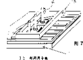
图7是设置在前玻璃基板1上的引线插脚6的熔接部分附近的封闭用导板15的说明图,FIG. 7 is an explanatory diagram of a sealing
图8是前玻璃基板1的制造工序图,8 is a manufacturing process diagram of the
图9是图8之后的制造工序图,Fig. 9 is a manufacturing process diagram following Fig. 8,
图10是后玻璃基板10的制造工序图,10 is a manufacturing process diagram of the
图11是将前玻璃基板1和后玻璃基板10嵌合起来组装成显示屏并进行密封的最后工序图,Fig. 11 is a diagram of the final process of assembling the
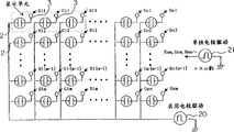
图12是说明本发明的实施形态2的平面显示屏的控制装置的图,是将各显示单元作为放电管表示的显示屏的等效电路图,12 is a diagram illustrating a control device for a flat display panel according to
图13是说明本发明的实施形态2的平面显示屏的控制装置的图,是驱动电路的方框结构图,13 is a diagram illustrating a control device for a flat display panel according to
图14是由图13中的驱动电路进行的亮度等级显示用的加在各电极上的驱动波形图,Fig. 14 is the driving waveform diagram applied on each electrode for brightness level display by the driving circuit in Fig. 13,
图15是表示图13的变形例的驱动电路的方框结构图,FIG. 15 is a block diagram showing a drive circuit of a modified example of FIG. 13,
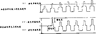
图16是由图14中的驱动电路进行的亮度等级显示用的加在各电极上的驱动波形图及其说明图,Fig. 16 is the driving waveform diagram and its explanatory diagram added on each electrode for brightness level display by the driving circuit in Fig. 14,
图17是说明本发明的实施形态2的平面显示屏的系统结构图,Fig. 17 is a system configuration diagram illustrating a flat display panel according to
图18是说明本发明的实施形态2的平面显示屏的控制装置的图,表示将控制信号供给在图17中以级联方式连接的各显示模块的驱动电路的信号处理电路的结构图,18 is a diagram illustrating a control device for a flat display panel according to
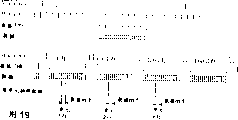
图19是说明图18所示的信号处理电路的工作的波形图,Fig. 19 is a waveform diagram illustrating the operation of the signal processing circuit shown in Fig. 18,
图20是说明图18所示的脉冲计数器56和一览表57及由显示数据生成部58进行单独电极控制用的与深淡等级数据生成有关的深淡等级显示处理的框图及流程图,FIG. 20 is a block diagram and a flow chart for explaining the pulse counter 56 and the table 57 shown in FIG. 18 and the gradation display processing related to the generation of gradation data for individual electrode control by the display
图21是图18所示的一览表57的输入输出特性曲线图,FIG. 21 is an input-output characteristic graph of the
图22是说明本发明的实施形态3的平面显示屏的驱动方法的单独电极驱动部的框图,Fig. 22 is a block diagram illustrating an individual electrode driving section of a method of driving a flat panel display according to
图23是说明本发明的实施形态3的平面显示屏的驱动方法的驱动时序图,Fig. 23 is a driving timing chart illustrating a method of driving a flat panel display according to
图24是说明本发明的实施形态3的平面显示屏的驱动方法的显示屏的工作说明图,Fig. 24 is an explanatory view showing the operation of the display panel for explaining the driving method of the flat display panel according to
图25是说明本发明的实施形态3的平面显示屏的驱动方法的显示屏的工作说明图,Fig. 25 is an explanatory view showing the operation of the display panel for explaining the driving method of the flat display panel according to
图26是说明本发明的实施形态3的平面显示屏的驱动方法的显示单元的初始化工作说明图,Fig. 26 is an explanatory diagram illustrating an initialization operation of a display unit in a driving method of a flat display panel according to
图27是说明本发明的实施形态3的平面显示屏的驱动方法的放电工作说明图,Fig. 27 is an explanatory diagram of a discharge operation for explaining a driving method of a flat panel display according to
图28是说明本发明的实施形态3的平面显示屏的驱动方法的显示单元的控制特性曲线图,Fig. 28 is a graph illustrating the control characteristics of the display unit of the driving method of the flat display panel according to
图29是说明本发明的实施形态3的平面显示屏的驱动方法的显示单元的控制特性曲线图,Fig. 29 is a graph illustrating the control characteristics of the display unit of the driving method of the flat display panel according to
图30是说明本发明的实施形态3的平面显示屏的驱动方法的脉冲发生电路的电路图,30 is a circuit diagram of a pulse generating circuit illustrating a method of driving a flat panel display according to
图31是说明本发明的实施形态3的平面显示屏的驱动方法的显示单元的控制特性曲线图,Fig. 31 is a graph illustrating the control characteristics of the display unit of the driving method of the flat display panel according to
图32是说明本发明的实施形态3的平面显示屏的驱动方法的深淡等级显示控制的时序图。Fig. 32 is a timing chart illustrating gradation display control in the driving method of the flat display panel according to
具体实施方式Detailed ways
实施形态1
图1是表示本发明的实施形态1的平面显示屏的总体的概略结构图。Fig. 1 is a schematic configuration diagram showing the whole of a flat display panel according to
如图1所示,作为本实施形态的平面显示屏的彩色扁平屏是一种显示部和驱动部构成一体的使用方便的显示屏,将由四个64点的显示屏A构成的256点显示单元作为基准,在各显示屏的背面侧设有端子变换基板B及单独电极驱动电路C,对该四个显示屏A设置脉冲电路/信号处理电路D。As shown in Figure 1, the color flat screen as the flat display screen of this embodiment is a display unit with an easy-to-use display unit and a drive unit integrated, and a 256-point display unit composed of four 64-point display screens A As a reference, a terminal conversion substrate B and an individual electrode drive circuit C are provided on the back side of each display panel, and a pulse circuit/signal processing circuit D is provided for the four display panels A.
图2和图3是分别表示作为构成上述显示屏的第一透明基板的前玻璃基板上的和作为第二基板的后玻璃基板上的结构的局部斜视图,另外图4是图3中的a-a’线剖面图,图5是表示后玻璃基板上的排气槽的结构图。Fig. 2 and Fig. 3 are the partial oblique views showing respectively the structure on the front glass substrate as the first transparent substrate constituting the above-mentioned display screen and on the rear glass substrate as the second substrate, and Fig. 4 is a in Fig. 3 in addition - a' line sectional view, Fig. 5 is a structural view showing the exhaust groove on the rear glass substrate.
如图2(a)所示,在前玻璃基板1上并列设置多个由共用电极2和单独电极3构成的一对电极,构成电极组,上述共用电极2用来一并地驱动构成显示画面的全部显示单元或部分地驱动任意的显示单元,上述单独电极3用来单独驱动构成显示画面的每一个显示单元。As shown in Figure 2(a), a pair of electrodes consisting of
另外,设有覆盖这些一对电极而成的电介质层4及保护膜层5,在对应于构成显示画面的显示单元之间的位置的单独电极3上竖直地设置引出电极用的引线插脚6。另外,3b是连接在单独电极3的母电极3a或共用电极2上的透明电极。In addition, a
另外,如图2(b)所示,在前玻璃基板1上与单独电极3的引线插脚6相同,在与显示单元之间的位置对应的共用电极2上竖直地设置引出电极用的引线插脚7,这些引线插脚6和7分别利用与上述单独电极3及上述共用电极2的材料相同的金属材料为主要成分的膏或接合材料分别熔接在上述单独电极3的母电极3a及上述共用电极2上。另外,在表示共用电极的引线插脚的引出部分附近的图2(b)中,虚线部分表示电介质层4下面的电极图形。In addition, as shown in FIG. 2(b), on the
另一方面,如图3及图4所示,在与设置在上述前玻璃基板1上的上述共用电极2及单独电极3相对的后玻璃基板10的对应部分上分别刻蚀出呈矩形的具有所希望的深度的凹部11,形成各显示单元的放电空间,在该凹部11的底面上通过用白色玻璃或金属构成的反射层(图中未示出)涂敷红、绿、蓝色的荧光体层12a、12b、12c。另外,在该后玻璃基板10上,在与上述引线插脚6及7对应的位置上刻蚀出电极引出用通孔13,用来将上述引线插脚6及7引出到显示画面的背面一侧。On the other hand, as shown in FIG. 3 and FIG. 4 , on the corresponding parts of the
另外,上述凹部11的深度T为参与放电的一个显示单元内的共用电极和单独电极的间隙t的三倍以上,上述间隙t通常为100微米,故T被刻蚀成300~600微米,使得放电空间的厚度较厚,能提高亮度。In addition, the depth T of the above-mentioned
另外,如图5所示,在由因刻蚀而设置在后玻璃基板10上的凹部11形成的各显示单元的放电空间之间设有排气槽14,与在后玻璃基板上形成的后文所述的排气用通孔联通,能确保真空排气时杂质气体的通路。In addition, as shown in FIG. 5, an
将如上构成的前玻璃基板1和后玻璃基板10嵌合起来,使在前玻璃基板1上竖直设置的引线插脚经过后玻璃基板10上的通孔伸出到外部,组装成显示屏并进行密封,而这时如图6所示,由于引线插脚6由被熔接在电极上的下端部6a和细长的前端部6b构成,6a的直径比6b的直径大,将插入电极引出用通孔13形成由上述引线插脚6的下端部6a插入的大直径部分13a和延伸出上述引线插脚6的前端部6b的小直径部分13b的两段构成的台阶状,所以引线插脚6定位后能防止前玻璃基板1和后玻璃基板10之间的无用的间隙。另外,引线插脚7呈同样的形状。The
另外,如图7所示,在上述前玻璃基板1上的引线插脚6的熔接部分附近设有封闭用的导板15,用来防止密封材料在密封上述前玻璃基板1和后玻璃基板10时流入显示单元,所以能防止密封材料流入放电单元。In addition, as shown in Figure 7, a
其次,说明具有如上结构的平面显示屏的制造方法。Next, a method of manufacturing the flat panel display having the above structure will be described.
图8至图11表示平面显示屏的制造工序,图8和图9是前玻璃基板1的制造工序图,图10是后玻璃基板10的制造工序图,图11是将前玻璃基板1和后玻璃基板10嵌合起来组装成显示屏进行密封的最后工序图。Fig. 8 to Fig. 11 represent the manufacturing process of flat display screen, Fig. 8 and Fig. 9 are the manufacturing process figure of
参照图8及图9说明前玻璃基板1的制造工序。The manufacturing process of the
首先,如图8(a)所示,对在全部表面上设置了单独电极的透明电极部分的前玻璃基板1经过刻蚀工序进行透明电极的图形刻蚀,形成如图8(b)所示的透明电极图形。First, as shown in FIG. 8(a), the
此后,如图8(c)所示,利用丝网印刷法形成共用电极2及单独电极3的母电极。Thereafter, as shown in FIG. 8( c ), the
另外,接着如图9(d)所示,利用丝网印刷法在共用电极2及单独电极3上覆盖一层由设置共用电极2及单独电极3的电极取出用窗口的绝缘体形成的电介质层4。In addition, as shown in FIG. 9( d ), the
此后,如图9(e)所示,通过电极取出用窗口将引线插脚6及7竖直地设置在共用电极及单独电极上,然后再利用真空蒸镀法形成保护膜层5。Thereafter, as shown in FIG. 9( e ), the lead pins 6 and 7 are vertically arranged on the common electrode and the individual electrodes through the electrode extraction window, and then the
另外,参照图10说明后玻璃基板10部分的制造工序。In addition, a manufacturing process of the
首先,如图10(b)所示,利用喷砂法对图10(a)所示的后玻璃基板10进行刻蚀,在该玻璃基板上刻蚀出形成构成显示画面的各显示单元的放电空间用的凹部11、将在上述共用电极2及上述单独电极3上竖直设置的引线插脚7及6分别引出到显示画面的背面一侧的电极引出用通孔13a及13b、以及与上述排气槽14联通的排气用通孔15。First, as shown in FIG. 10(b), the
然后,如图10(c)所示,利用丝网印刷法在形成显示单元的各凹部11的底面上通过用白色玻璃或金属构成的反射层(图中未示出)形成红、绿、蓝色的荧光体层12a、12b、12c。Then, as shown in FIG. 10(c), red, green, and blue colors are formed on the bottom surface of each
其次,如图11(a)所示,将这样来构成的前玻璃基板1部分和后玻璃基板10部分组装成屏,使前玻璃基板1上的引线插脚6及7经过后玻璃基板10上的通孔13伸出到外部嵌合起来,如图11(b)所示,用玻璃原料涂敷组装后的这些基板进行密封,形成密封层16,制成显示屏。另外,17是排气用的玻璃管。Next, as shown in Fig. 11 (a), the
因此,如果采用上述实施形态1,则由于备有:第一透明基板、在该第一透明基板上设置的一对电极、以及在与上述一对电极对应的部分形成凹部而构成显示单元的放电空间的第二基板,所以能获得显示屏的每个显示单元都能单独驱动、而且具有能使平面厚度变薄的放电空间结构的平面显示屏。Therefore, if the above-mentioned first embodiment is adopted, since the first transparent substrate, the pair of electrodes provided on the first transparent substrate, and the recesses are formed in the portions corresponding to the pair of electrodes, the discharge of the display unit is constituted. The second substrate of the space, so each display unit of the display screen can be driven independently, and a flat display screen with a discharge space structure that can make the plane thickness thinner can be obtained.
另外,由于在上述第一透明基板上并列设置多对电极以构成电极组,所以能容易地形成多个放电单元的电极结构。In addition, since a plurality of pairs of electrodes are arranged in parallel on the first transparent substrate to form an electrode group, an electrode structure of a plurality of discharge cells can be easily formed.
另外,上述凹部呈矩形且具有所希望的深度,所以不设置区分放电空间用的隔壁、而且能在与电极的形成无关的情况下直接形成放电空间,使显示屏的平面厚度变薄。In addition, the concave portion has a rectangular shape and a desired depth, so that no barrier ribs are provided for partitioning the discharge space, and the discharge space can be directly formed regardless of the formation of electrodes, thereby reducing the planar thickness of the display panel.
另外,上述凹部的深度在300~600微米的范围内,所以放电空间的厚度较厚,能提高亮度。In addition, since the depth of the concave portion is in the range of 300 to 600 micrometers, the thickness of the discharge space is relatively thick, and the luminance can be improved.
另外,在上述第一透明基板上设有覆盖上述一对电极的电介质层,所以能防止电荷向外部扩散,能将电荷封闭在放电单元内。In addition, since the dielectric layer covering the pair of electrodes is provided on the first transparent substrate, the charge can be prevented from being diffused to the outside, and the charge can be enclosed in the discharge cell.
另外,由于将荧光体层设置在上述第二基板的上述凹部的底面上,所以能容易地进行彩色显示,能获得均匀的亮度,图象具有均匀性。In addition, since the phosphor layer is provided on the bottom surface of the concave portion of the second substrate, color display can be easily performed, uniform brightness can be obtained, and the image has uniformity.
另外,由于在上述第二基板的上述凹部的底面和上述荧光体层之间设有反射层,所以能使荧光体发的光向前面射出。In addition, since the reflective layer is provided between the bottom surface of the concave portion of the second substrate and the phosphor layer, light emitted by the phosphor can be emitted to the front.
另外,由于上述一对电极包括设置在上述第一透明基板上而且一并地同时驱动构成显示画面的全部显示单元或部分地同时驱动任意多个显示单元的共用电极以及设置在上述第一透明基板上而且单独驱动构成显示画面的每一个显示单元的单独电极,因此提供一种能单独驱动显示屏的每一个显示单元、而且具有能使平面厚度变薄的电极结构的平面显示屏。In addition, since the above-mentioned pair of electrodes includes a common electrode that is arranged on the above-mentioned first transparent substrate and simultaneously drives all the display units constituting the display screen or partially simultaneously drives any number of display units, and is arranged on the above-mentioned first transparent substrate. and independently drive the individual electrodes of each display unit constituting the display screen, thus providing a flat panel display capable of individually driving each display unit of the display panel and having an electrode structure capable of reducing the plane thickness.
另外,由于在上述第二基板上形成的凹部的深度为参与放电的一个显示单元内的共用电极和单独电极的间隙的三倍以上,所以使得放电空间的厚度较厚,能提高亮度。In addition, since the depth of the concave portion formed on the second substrate is more than three times the gap between the common electrode and the individual electrode in a display unit participating in the discharge, the thickness of the discharge space is thicker, and the brightness can be improved.
另外,由于在上述第二基板上形成的各显示单元之间设有排气槽,同时在上述第二基板上设有与上述排气槽联通的排气用通孔,所以能确保真空排气时的杂质气体的通路。In addition, since exhaust grooves are provided between the display units formed on the second substrate, and exhaust through holes communicating with the exhaust grooves are provided on the second substrate, it is possible to ensure vacuum exhaust. The passage of impurity gas during the time.
另外,由于将引线插脚竖直地设置在上述共用电极和上述单独电极上,其中上述共用电极和上述单独电极设置在构成上述第一透明基板上的显示画面的显示单元之间的位置上,同时在上述第二基板上与上述引线插脚相对的位置设有电极引出用通孔,用来将上述引线插脚引出到显示画面的背面一侧,所以能容易地将电极引出到显示画面的背面一侧。In addition, since the lead pins are vertically arranged on the above-mentioned common electrode and the above-mentioned individual electrode, wherein the above-mentioned common electrode and the above-mentioned individual electrode are arranged at positions between the display units constituting the display screen on the above-mentioned first transparent substrate, at the same time On the above-mentioned second substrate, the position opposite to the above-mentioned lead pin is provided with a through hole for drawing out the electrode, which is used to lead out the above-mentioned lead pin to the back side of the display screen, so the electrodes can be easily drawn out to the back side of the display screen. .
另外,由于上述引线插脚利用与上述共用电极和上述单独电极的母电极材料相同的金属材料为主要成分的膏或接合材料熔接在上述共用电极和上述单独电极的母电极上,所以能将引线插脚牢固地固定在电极上。In addition, since the above-mentioned lead pin is welded on the above-mentioned common electrode and the base electrode of the above-mentioned individual electrode using the same metal material as the paste or bonding material of the above-mentioned common electrode and the base electrode material of the above-mentioned individual electrode, it is possible to connect the lead pin Securely affixed to electrodes.
另外,由于上述引线插脚有被熔接在电极上的直径大的下端部分,上述电极引出用通孔有能将上述引线插脚的下端部分插入的直径大的部分,以及能使上述引线插脚的前端部分伸出的直径小的部分,且由这两部分形成台阶形状,所以能容易地进行引线插脚的定位,同时能防止发生第一及第二玻璃基板的无用的间隙。In addition, since the above-mentioned lead pin has a large-diameter lower end portion welded to the electrode, the above-mentioned electrode drawing-out through hole has a large-diameter portion into which the lower end portion of the above-mentioned lead pin can be inserted, and the front end portion of the above-mentioned lead pin can be Since the protruding portion has a small diameter, and these two portions form a stepped shape, the positioning of the lead pins can be easily performed, and useless gaps between the first and second glass substrates can be prevented.
另外,由于在上述引线插脚的熔接部附近设有上述第一及第二基板密封时封闭用的导板,所以能防止密封材料流入显示单元。In addition, since the guide plate for sealing the first and second substrates is provided near the welded portion of the lead pins, the sealing material can be prevented from flowing into the display unit.
另外,如果采用该实施形态1,则由于包括以下工序:在第一透明基板上对单独电极的透明电极进行图形刻蚀的工序;在形成上述透明电极的第一透明基板上形成单独电极和共用电极的母电极的工序;形成将上述第一透明基板上的单独电极和共用电极覆盖起来的电介质层的工序;通过上述电介质层上的电极引出窗口将引线插脚竖直设置在上述单独电极和上述共用电极上的插脚安装工序;以及经过上述插脚安装工序后在上述第一透明基板上形成保护膜层的工序,同时还有:刻蚀在上述第二基板上形成构成显示画面的各显示单元的放电空间用的凹部和刻蚀将在上述共用电极及上述单独电极上竖直设置的引线插脚引出到显示画面的背面一侧的电极引出用通孔及排气用通孔的工序以及在形成上述显示单元的各凹部的底面上形成荧光体层的工序,而且还有:将经过了这些工序后的第一透明基板上的引线插脚经过第二基板上的通孔延伸到外部,并将该第一和第二基板嵌合起来组装屏的工序以及密封组装后的第一和第二基板的工序,所以能单独驱动显示屏的每一个显示单元,而且容易获得具有能使平面厚度变薄的电极结构的平面显示屏。In addition, if this embodiment 1 is adopted, since it includes the following steps: a process of pattern-etching the transparent electrodes of the individual electrodes on the first transparent substrate; The process of the mother electrode of the electrode; the process of forming a dielectric layer covering the individual electrodes and the common electrode on the first transparent substrate; vertically setting the lead pins on the above-mentioned individual electrodes and the above-mentioned electrodes through the electrode lead-out window on the above-mentioned dielectric layer The pin installation process on the common electrode; and the process of forming a protective film layer on the first transparent substrate after the above pin installation process, and at the same time: etching on the second substrate to form each display unit constituting the display screen Recess for the discharge space and the process of etching the lead pins vertically provided on the above-mentioned common electrode and the above-mentioned individual electrode to the through-hole for electrode extraction and the through-hole for exhaust on the back side of the display screen and the process of forming the above-mentioned The process of forming a phosphor layer on the bottom surface of each concave portion of the display unit, and furthermore: extending the lead pins on the first transparent substrate after these processes to the outside through the through holes on the second substrate, and extending the first transparent substrate to the outside. The process of assembling the screen with the second substrate and the process of sealing the assembled first and second substrates, so that each display unit of the display can be driven independently, and it is easy to obtain an electrode with a thinner plane thickness. Structured flat display.
实施形态2
如果采用上述实施形态1,则使前玻璃基板1上的引线插脚6及7经过后玻璃基板10上的通孔13伸出到外部那样地嵌合起来,将前玻璃基板1和后玻璃基板10组装成屏,用玻璃料涂敷组装后的这些基板进行密封,形成密封层16,制成显示屏,能获得能单独驱动显示屏的每一个显示单元、而且具有能使平面厚度变薄的电极结构的平面显示屏,而在该实施形态2中,将详细说明驱动控制具有如上所述的电极结构的平面显示屏的控制装置。If adopt above-mentioned
图12是将各显示单元作为放电管表示的平面显示屏的等效电路图。Fig. 12 is an equivalent circuit diagram of a flat display panel in which each display unit is represented as a discharge tube.
如图12所示,以涂敷了红、绿、蓝色的荧光体层的三个单元为单位,将其作为与一个象素对应的一个显示单元,平面显示屏备有多个这样的一个显示单元,将来自共用电极驱动部20的同一驱动波形脉冲供给各单元的共用电极2,从单独电极驱动部21将各个单独的驱动波形脉冲供给作为各个单独电极3的单独电极Rnm、Gnm、Bnm(n、m是自然数)。As shown in Figure 12, three units coated with red, green, and blue phosphor layers are used as a display unit corresponding to one pixel, and a flat panel has a plurality of such units. The display unit supplies the
另外,在共用电极一并地驱动一个屏的情况下,用同一驱动波形驱动各个单元。另外,在将一个显示屏分隔成多个块而使用多个共用电极的情况下,用同一驱动波形或使显示驱动部的相位在每个块中发生偏移的驱动波形进行驱动。In addition, in the case of collectively driving one panel with a common electrode, each cell is driven with the same driving waveform. Also, when one display panel is divided into a plurality of blocks and a plurality of common electrodes are used, driving is performed with the same driving waveform or a driving waveform in which the phase of the display driving unit is shifted for each block.
图13表示由上述共用电极驱动部20及上述单独电极驱动部21构成的驱动电路的方框结构图,它表示驱动两个象素六个单元的情况。FIG. 13 is a block diagram showing a driving circuit composed of the above-mentioned common
如图13所示,作为连接各个共用电极2并供给驱动脉冲的共用电极驱动部20的结构备有:由连接在电源350V上的开路漏极的FET构成的开关元件Q1;被施加200V电压的二极管D1;由对称地连接的特性相同的FET而成的推挽驱动型的开关元件Q2及Q3构成的开关控制部20a;以及将控制脉冲供给这些开关元件Q1~Q3的栅极的共用电极一侧控制脉冲供给部20b。As shown in FIG. 13 , as the structure of the common
另外,作为单独电极驱动部21的结构备有:由在电源200V和接地端GND之间相对于作为单独电极3的每个单独电极R11、G11、B11、R21、G21、B21对称地连接的特性相同的FET而成的推挽驱动型的开关元件QR11a和QR11b、QG11a和QG11b、QB11a和QB11b、QB21a和QB21b、QG21a和QG21b、QR21a和QR21b构成的开关控制部21a;以及将控制脉冲供给这些开关元件的栅极的单独电极一侧的控制脉冲供给部21b。In addition, as the structure of the individual
图14表示由上述的驱动电路产生的显示亮度等级用的加在各电极上的波形。Fig. 14 shows the waveforms applied to the respective electrodes for displaying gradation of brightness generated by the driving circuit described above.
该显示屏相对于输入脉冲基本上只能取双值工作(显示/不显示)的两种状态。通过施加连续的维持显示脉冲进行显示,用在加在共用电极上的脉冲-脉冲之间的期间内插入、在单位时间内加在单独电极上的脉冲数来控制亮度的变化(深淡等级)。Compared with the input pulse, the display screen can basically only take two states of double-value work (display/non-display). Display is performed by applying continuous sustain display pulses, and the number of pulses applied to individual electrodes per unit time is used to control the change in brightness (gradation) .
如图14所示,通过将来自控制脉冲供给部20b的脉冲供给共用电极2,使开关元件Q1和Q2导通,使开关元件Q3截止,供给350V的点火脉冲,开始放电,此后使开关元件Q1截止,使开关元件Q2和Q3导通/截止,供给下降到200V的维持显示脉冲。As shown in FIG. 14, by supplying the pulse from the control
对单独电极确定一个时序内的脉冲数,在全部脉冲被加在单独电极上的情况下,达到最高亮度,通过减少加在单独电极上的脉冲数,使由该单独电极驱动的单元的亮度下降。Determine the number of pulses in a time sequence for a single electrode. When all pulses are applied to a single electrode, the highest brightness is achieved. By reducing the number of pulses applied to a single electrode, the brightness of the unit driven by the single electrode is reduced. .
例如,将127次的脉冲供给单独电极R11,能控制127深淡等级的亮度;在n深淡等级的情况下将n次的脉冲供给单独电极G11,能控制最大亮度;将1次脉冲供给单独电极B11,能控制描绘最暗时的一种深淡等级;停止对单独电极R21供给脉冲,则呈非点亮状态;同样,将127次的脉冲供给单独电极G21,能控制127深淡等级的亮度;将1次脉冲供给单独电极B21,能控制1次的亮度。For example, if 127 pulses are supplied to the individual electrode R11, the brightness of 127 shading levels can be controlled; in the case of n shading levels, n times of pulses are supplied to the individual electrode G11, and the maximum brightness can be controlled; 1 pulse is supplied to the individual electrode G11. Electrode B11 can control a shading level when drawing the darkest state; stop supplying pulses to the individual electrode R21, it will be in a non-lighting state; similarly,
因此,单独电极的工作是在显示期间中施加对应于能维持放电显示的深淡等级数的脉冲,在非显示期间进行停止施加维持脉冲的控制。另外,在将最后一个脉冲输入到单独电极后至下一个脉冲加在共用电极上之前进行发光显示,在停止向单独电极施加脉冲后,即使向共用电极输入脉冲,也不发光。Therefore, the operation of the individual electrodes is to apply pulses corresponding to the number of gradation levels capable of sustaining discharge display during the display period, and control to stop application of sustain pulses during the non-display period. In addition, luminous display is performed after the last pulse is input to the individual electrode and before the next pulse is applied to the common electrode, and no light is emitted even if the pulse is input to the common electrode after the pulse application to the individual electrode is stopped.
另外,图15表示图13所示的驱动电路的变形例。In addition, FIG. 15 shows a modified example of the drive circuit shown in FIG. 13 .
图15所示的驱动电路相对于图13所示的驱动电路来说,开关控制部的结构不同。即,作为开关控制部,除了对称地连接被连接在电源200V和接地端GND之间的特性相同的FET而形成的推挽驱动型的开关元件构成的单独电极驱动开关部21aa以外,还备有由对称地连接被连接在电源200V和接地端GND之间的特性相同的FET而形成的推挽驱动型的开关元件构成的一并驱动开关部21ab,以及分别设置在单独电极驱动开关部21aa和一并驱动开关部21ab的各一对FET的连接点之间的二极管的反向并联连接体组21ac。The drive circuit shown in FIG. 15 is different from the drive circuit shown in FIG. 13 in the structure of the switch control unit. That is, as the switch control unit, in addition to the individual electrode drive switch unit 21aa formed by symmetrically connecting FETs with the same characteristics connected between the
图16是表示上述的图15所示的驱动电路产生的显示亮度等级用的供给各电极的驱动波形的说明图。FIG. 16 is an explanatory diagram showing driving waveforms supplied to respective electrodes for displaying luminance levels generated by the driving circuit shown in FIG. 15 described above.
为了进行放电显示,在施加维持脉冲后,为了有助于下一次放电显示,需要一定时间的电压维持时间。如果不维持该电压,而将脉冲切断时,就会抑制下一次的放电发光。In order to perform a discharge display, after a sustain pulse is applied, a certain voltage maintenance time is required to contribute to the next discharge display. If the voltage is not maintained and the pulse is cut off, the next discharge light emission will be suppressed.
利用该现象,通过进行对单独电极施加宽度较宽的维持脉冲的波形和施加宽度较窄的短时间的维持脉冲(消除脉冲)的情况的控制,能进行深淡等级显示。Utilizing this phenomenon, gradation display can be performed by controlling the application of a broad sustain pulse waveform and a narrow short sustain pulse (erase pulse) to individual electrodes.
即,如图16(a)所示,在最大亮度时,相对于加到单独电极上的全部脉冲来说,将宽度较宽的脉冲供给单独电极(参照单独电极G11的波形),而对中等亮度的单元来说,则从时序的中期开始将宽度窄的消除脉冲供给单独电极(参照单独电极R11、G21的波形)。That is, as shown in FIG. 16(a), at the time of maximum luminance, a pulse having a wider width is supplied to the individual electrode (refer to the waveform of the individual electrode G11) relative to all the pulses applied to the individual electrode, while for the medium In units of luminance, a narrow erasing pulse is supplied to the individual electrodes from the middle of the timing (see the waveforms of the individual electrodes R11 and G21).
因此,在施加了宽度窄的消除脉冲期间,不进行放电显示。其结果,显示亮度下降,达到中等亮度。另外,通过将适当的宽度窄的脉冲加在单独电极上,能做到不能用共用电极的脉冲进行发光。Therefore, discharge display is not performed while a narrow erasing pulse is applied. As a result, the display luminance drops to a moderate luminance. In addition, by applying pulses with appropriate narrow widths to individual electrodes, it is possible to achieve light emission that cannot be achieved with pulses from a common electrode.
这里,如图16(a)中的局部放大图所示,宽度较宽的维持脉冲有期间I和II的宽度,另外,宽度较窄的维持脉冲有期间I的宽度。另外,,如图16(b)所示,通过对一并驱动开关部21ab和单独电极驱动开关部21aa进行开关控制,能够实现这些期间I和II、宽度较宽的维持脉冲和宽度较窄的维持脉冲之间的期间III、以及宽度较窄的维持脉冲施加后的期间IV。Here, as shown in the partial enlarged view in FIG. 16( a ), the wide sustain pulse has the width of periods I and II, and the narrow sustain pulse has the width of period I. In addition, as shown in FIG. 16(b), these periods I and II, wider sustain pulses, and narrower sustain pulses can be realized by performing switching control on the collective drive switch section 21ab and the individual electrode drive switch section 21aa. Period III between sustain pulses and period IV after application of a narrow sustain pulse.
例如将期间I控制成使一并驱动开关部21ab的高边侧FET导通、使低边侧FET截止,且控制成使单独电极驱动开关部21aa的高边侧FET截止、使低边侧FET截止。另外,将期间II控制成使一并驱动开关部21ab的高边侧FET截止、使低边侧FET截止,且控制成使单独电极驱动开关部21aa的高边侧FET导通、使低边侧FET截止。另外,期间III及IV同样如图16(b)所示进行控制。For example, the period I is controlled to turn on the high-side FET of the collectively driven
其次,图17是平面显示屏的系统结构图。Secondly, FIG. 17 is a system structure diagram of the flat display screen.
如图17所示,将四个8×8点的(2×2)显示单元组合而成的显示模块30作为结构要素构成显示部,各显示模块30沿列方向(扫描线方向)排列的模块之间以级联方式连接,共有图象信号、控制信号。As shown in FIG. 17, a
另外,电源40与每个显示模块30并联连接,以便通过并联供电,在显示模块30之间不产生电压降。In addition, the power supply 40 is connected in parallel with each
图18是表示将控制信号供给以级联方式连接的各显示模块的驱动电路的信号处理电路的结构图。18 is a configuration diagram showing a signal processing circuit that supplies a control signal to a driver circuit of each display module connected in cascade.
图18所示的信号处理电路50备有:存储固有地址信息的模块地址信息存储部51;在使输入的数据通过的同时,与上述固有地址一起从数据中的有效显示信号的位置取出自行显示的数据用的输入信号控制/显示控制部52;将从上述输入信号控制/显示控制部52通过的数据输出给以级联方式连接的相邻的显示模块用的通过数据用输出缓冲器53;根据写入控制信号写入由上述输入信号控制/显示控制部52取出的数据、同时根据读出控制信号进行数据的读出的存储器54;根据由上述输入信号控制/显示控制部52取出的数据生成共用电极及单独电极驱动脉冲的显示用脉冲生成器55;对从上述显示用脉冲生成器55输出的共用电极驱动脉冲进行计数的计数器56;将由脉冲计数器56计数的脉冲数变换成深淡等级数据用的一览表57;根据通过了上述一览表57的深淡等级数据和从存储器54读出的单独电极驱动用显示数据的比较结果,输出单独电极的控制数据的显示数据生成器58;将上述显示用脉冲生成器55及上述显示数据生成器58的输出信号输出给单独电极驱动电路及共用电极驱动电路的输出缓冲器59;以及将时钟脉冲供给上述显示用脉冲生成器55的时钟脉冲生成器60。另外,DATA(R)、DATA(G)、DATA(B)分别表示由8位构成的RGB数据,Vsync表示垂直同步信号,Hsync表示水平同步信号,DENB表示允许数据传送信号,DCLK表示同步信号。The
以级联方式连接的横向排列的各显示模块30各自的固有模块地址预先被送给模块地址信息存储部51。另外,显示及显示控制用的信号通过相邻的显示模块输出,该通过的数据信号被供给输入信号控制/显示控制部52。The unique module addresses of the horizontally arranged
如图19所示,输入信号控制/显示控制部52根据固有地址数据和数据中的有效显示信号(DATA、ENB)、以及垂直、水平同步信号,计算自行显示模块显示的数据的开始位置,从该位置开始将显示数据存入抽样存储器54。As shown in Figure 19, the input signal control/
具体地说,首先从固有地址信息中找出垂直、水平方向的自行显示模块位置。这一点通过固有地址具有显示模块被配置在相对于垂直、水平方向的哪个位置的信息来实现,固有地址的水平方向位置、垂直方向位置是将固有地址各自的位置信息乘以与显示模块的象素数对应的16算得的数值。Specifically, first find out the position of the self-display module in the vertical and horizontal directions from the inherent address information. This is achieved by the unique address having information about where the display module is arranged relative to the vertical and horizontal directions. The horizontal and vertical positions of the unique address are obtained by multiplying the respective position information of the unique address with the image of the display module The calculated value of 16 corresponding to a prime number.
水平方向位置是这样的位置,即在水平同步信号输入后对从ENB变为有效的时刻开始的点时钟脉冲进行计数,在到达固有地址中规定的位置(计数值)之前使数据通过,从到达了规定位置的时钟脉冲开始对16个象素的数据抽样后,再使以后的数据通过。The position in the horizontal direction is the position at which the dot clock pulses from the time when ENB becomes valid are counted after the horizontal synchronizing signal is input, and the data is passed until it reaches the position (count value) specified in the unique address. After the clock pulse at the specified position begins to sample the data of 16 pixels, the subsequent data is passed.
对于垂直方向位置来说,也与水平位置信息一样,通过垂直同步信号的输入使垂直方向的行计数器复位。在其计数值到达固有地址中规定的位置(计数值)之前使数据通过,从到达了规定位置的时钟脉冲开始对16个象素的数据抽样后,再使以后的数据通过。As for the position in the vertical direction, as in the horizontal position information, the line counter in the vertical direction is reset by the input of the vertical synchronizing signal. The data is passed before the count value reaches the position (count value) specified in the unique address, and the data of 16 pixels is sampled from the clock pulse that has reached the specified position, and then the subsequent data is passed.
通过对该水平方向、垂直方向的处理进行组合,将显示模块显示的数据中的16×16象素的数据写入存储器54。该存储器54由两部分构成,包括写入来自外部的显示信号的存储部分和显示时进行读出的存储部分。通常,两个存储单元与切换写入、读出的显示时的同步信号相一致、交替地执行各自的任务。By combining the processing in the horizontal direction and the vertical direction, the data of 16×16 pixels among the data displayed by the display module is written into the memory 54 . The memory 54 is composed of two parts, including a storage part for writing an external display signal and a storage part for reading out during display. Normally, the two memory cells perform their respective tasks alternately in accordance with a synchronous signal at the time of switching between writing and reading display.
如果采用图18所示的结构,将固有的地址送给各显示单元,在将显示单元组合起来时,能构成各个显示单元的位置信息,根据所输入的显示数据、同步数据来存储自行显示模块应显示的数据,能根据该数据进行显示控制,同时能识别各个显示模块。因此,通过经由数据总线传送显示模块的固有地址和控制数据,只有被指定的显示模块才能接收控制数据,能实现这样的各模块的控制,在到达固有地址中规定的位置(计数值)之前,使数据通过,从到达规定位置的时钟脉冲开始对16个象素的数据抽样后,再让以后的数据通过。If the structure shown in Figure 18 is adopted, the inherent address is sent to each display unit, when the display units are combined, the position information of each display unit can be formed, and the self-display module is stored according to the input display data and synchronous data The data to be displayed can be displayed and controlled based on the data, and at the same time, each display module can be identified. Therefore, by transmitting the unique address and control data of the display module through the data bus, only the designated display module can receive the control data, and the control of each module can be realized. Before reaching the position (count value) specified in the unique address, To pass the data, the data of 16 pixels is sampled from the clock pulse reaching the predetermined position, and then the subsequent data is passed.
作为该显示控制的例,是通过在显示数据的消隐期间(数据无效时间)输入显示模块的固有地址和显示数据,例如能在模块中设定分别修正各模块之间的亮度离散的数据,能简化进行均匀显示用的调整工作,且容易维修。As an example of this display control, by inputting the unique address of the display module and the display data during the blanking period (data invalid time) of the display data, for example, the data for correcting the luminance dispersion between the modules can be set in the module, The adjustment work for uniform display can be simplified, and maintenance is easy.
图20(a)和(b)是说明与由上述脉冲计数器56和一览表57及显示数据生成部58进行单独电极控制用的深淡等级数据的生成有关的深淡等级处理的框图和流程图。20(a) and (b) are block diagrams and flowcharts illustrating gradation processing related to generation of gradation data for individual electrode control by the pulse counter 56, table 57, and
在显示模块内展开的图象数据的各色为256深淡等级(1670万种颜色)的情况下,与红(R)、绿(G)、蓝(B)数据一起作为8位的二进制数据从外部输入。由于该数据与显示模块的深淡等级表现不同,所以需要进行数据的格式变换。用维持脉冲数表现显示模块内的深淡等级级表现格式。因此,需要将输入的二进制格式的数据变换成脉冲数。In the case where the image data developed in the display module has 256 shades (16.7 million colors) for each color, 8-bit binary data together with red (R), green (G) and blue (B) data are from external input. Since the data is different from the shade level of the display module, it is necessary to convert the format of the data. Use the number of sustain pulses to express the display format of the shade level in the display module. Therefore, it is necessary to convert the input data in binary format into the number of pulses.
可是,通常在一个时序内输入的维持脉冲数不限于256个脉冲,所以不能只用二进制图象数据的大小作为显示数据。因此,需要有对维持脉冲进行计数的脉冲计数器56和比较二进制图象数据的大小时进行数值变换用的一览表57。However, generally, the number of sustain pulses input in one timing is not limited to 256 pulses, so only the size of binary image data cannot be used as display data. Therefore, a pulse counter 56 for counting sustain pulses and a table 57 for numerical conversion when comparing the size of binary image data are required.
一览表57对应于输入的数据,输出其大小具有一定的规则性的数据。The table 57 outputs data having a certain regularity in size corresponding to the input data.
图21是表示一览表57的输入输出特性的曲线图,对从计数器56输出的维持脉冲的10位(1024)的输入信号按上升的顺序分配0~255的值。其输入输出特性与维持脉冲数、输出值都是整数,所以呈分散的台阶状的曲线图,通过改变该曲线图的输入输出曲线,能将任意的维持脉冲数分配给输出值。21 is a graph showing the input/output characteristics of the table 57, in which values of 0 to 255 are assigned in ascending order to the 10-bit (1024) input signal of the sustain pulse output from the counter 56. The input and output characteristics, the number of sustain pulses, and the output value are all integers, so the graph in the form of scattered steps can assign any number of sustain pulses to the output value by changing the input and output curve of the graph.
通过使用对应于输入能自由地改变输出的一览表57,能将图象输入数据和维持脉冲数的大小的关系联系起来,能控制每一深淡等级的维持脉冲数,进行显示单元的亮度的调制。By using the table 57, which can freely change the output corresponding to the input, the relationship between the image input data and the number of sustain pulses can be linked, the number of sustain pulses for each shade level can be controlled, and the brightness of the display unit can be modulated. .
即,如图20(a)所示,由8位的比较器58R、58G、58B构成显示数据生成部58,例如在施加伴有放电显示的维持脉冲时,假定单独电极的控制数据为“1”(输出显示脉冲),进行呈非显示状态的控制时的数据为“0”(非显示状态),则如图20(b)所示,显示数据生成部58将由以计数器复位(与垂直同步输入同步)为依据对从显示用脉冲生成器55输出的共用电极驱动脉冲开始进行计数的十位计数器构成的脉冲计数器56的输出利用一览表57进行变换,并对变换后的值f(计数的维持脉冲数)和显示图象数据进行比较,求出That is, as shown in FIG. 20( a), the
f≤显示图象数据时,数据“1”When f≤display image data, data "1"
f>显示图象数据时,数据“0”f>When displaying image data, data "0"
对供给单独电极的每个脉冲的以对应于显示模块的单元数的次数反复进行该比较运算,直到处理完所有显示数据,将运算结果传送给对图13或图15所示的单独电极进行开关控制用的控制脉冲供给部,在下一个单独电极的脉冲的有无、脉冲形状、电压值等中反映出来。The comparison operation is repeated for each pulse supplied to the individual electrodes for the number of times corresponding to the number of units of the display module until all display data are processed, and the operation results are sent to the individual electrodes shown in Figure 13 or Figure 15. The control pulse supply unit for control is reflected in the presence or absence, pulse shape, voltage value, etc. of the pulse of the next individual electrode.
通过该控制,能对各个单元显示与输入的数据对应的亮度。Through this control, brightness corresponding to the input data can be displayed for each cell.
因此,如果采用上述实施形态2,则在备有一并地驱动构成显示画面的全部显示单元或部分地驱动任意的显示单元的共用电极以及逐个地单独驱动每个显示单元的单独电极的平面显示屏中,由于备有根据单位时间内加在上述单独电极上的脉冲数来改变亮度从而显示深淡等级的驱动电路,所以能对每个显示单元的独立的电极分别进行开关控制,从而进行深淡等级控制。Therefore, if the above-mentioned
另外,上述驱动电路作为在单位时间内加在上述单独电极上的脉冲,施加宽度较宽的维持脉冲和宽度较窄的消除脉冲,通过控制所施加的脉冲进行深淡等级显示,所以在施加消除脉冲期间能停止放电显示,能进行深淡等级显示。In addition, the above-mentioned drive circuit applies a wide-width sustain pulse and a narrow-width erase pulse as pulses applied to the above-mentioned individual electrodes in a unit time, and controls the applied pulses to perform gradation display. Therefore, when the erase pulse is applied, During the pulse period, the discharge display can be stopped, and the depth and light levels can be displayed.
另外,由于上述平面显示屏将把多个显示屏按行列排列组合的显示模块作为构成要素,沿列方向排列的显示模块以级联方式连接,而且各显示模块与电源并联连接,作为将控制信号供给各显示模块的驱动电路的信号处理电路,备有:存储固有地址信息的地址信息存储部;在使输入的数据通过的同时,与上述固有地址一起从数据中的有效显示信号的位置取出自行显示的数据用的输入信号控制部;将从上述输入信号控制部通过的数据输出给以级联方式连接的相邻的显示模块用的通过数据用输出缓冲器;根据写入控制信号写入由上述输入信号控制部取出的数据、同时根据读出控制信号进行数据的读出的存储器;根据由上述输入信号控制部取出的数据生成共用电极及单独电极驱动脉冲的显示用脉冲生成器;对从上述显示用脉冲生成器输出的共用电极驱动脉冲进行计数的计数器;将由上述计数器计数的脉冲数变换成深淡等级数据用的一览表;根据通过了上述一览表的深淡等级数据和从上述存储器读出的单独电极驱动用显示数据的比较结果,输出单独电极的控制数据的显示数据生成器;以及将上述显示用脉冲生成器及上述显示数据生成器的输出信号输出给单独电极驱动电路及共用电极驱动电路的输出缓冲器,所以在进行将显示模块组合时的数据控制的情况下,能取入与各显示模块的地址对应的显示数据,进行与数据对应的单独控制。In addition, since the above-mentioned flat display screen uses display modules arranged in rows and columns as constituent elements, the display modules arranged along the column direction are connected in cascade, and each display module is connected in parallel with the power supply as the control signal The signal processing circuit that is supplied to the drive circuit of each display module is equipped with: an address information storage unit that stores unique address information; while passing the input data, it extracts itself from the position of the effective display signal in the data together with the above-mentioned unique address. An input signal control unit for the displayed data; output the data passed from the above input signal control unit to an output buffer for passing data used by adjacent display modules connected in cascade; The data taken out by the above-mentioned input signal control part, and the memory for reading the data according to the read control signal at the same time; the display pulse generator for generating common electrode and individual electrode drive pulses according to the data taken out by the above-mentioned input signal control part; A counter for counting the common electrode drive pulses output by the above-mentioned display pulse generator; a table for converting the number of pulses counted by the above-mentioned counter into gradation data; The comparison result of the display data for driving the individual electrodes, the display data generator that outputs the control data for the individual electrodes; The output buffer of the circuit, so in the case of data control when display modules are combined, display data corresponding to the address of each display module can be taken in, and individual control corresponding to the data can be performed.
实施形态3
其次,在实施形态3中,说明具有用实施形态1说明的电极结构的平面显示屏的驱动方法。Next, in
在该实施形态3中,显示象素为10×10mm2,显示单元的大小为3×9mm2,共用电极2-单独电极3之间的电极间隙为100微米,另外,将500Torr的放电气体(Ne-Xe(5%))密封在高度为600微米的放电空间中。In
图22更详细地示出了图13所示的单独电极驱动部21的控制脉冲供给部21b的内部结构。另外,图23表示驱动平面显示屏用的驱动时序之一例。FIG. 22 shows in more detail the internal structure of the control pulse supply section 21b of the individual
本平面显示屏具有如图12所示的结构,所以需要一对共用电极驱动电路和与显示单元数相当的单独电极驱动电路。The flat display screen has the structure shown in Figure 12, so a pair of common electrode drive circuits and separate electrode drive circuits equivalent to the number of display units are required.
其次说明工作情况。Next, explain the working situation.
通常,如图24所示,在利用放电的平面显示屏中,将高压脉冲交替地加在一对电极上,这里是加在共用电极和与其在同一平面内相对的一个单独电极上,利用蓄积在放电单元的绝缘体上的壁电荷维持放电。Generally, as shown in Fig. 24, in a flat panel display using discharge, high-voltage pulses are alternately applied to a pair of electrodes, here a common electrode and a separate electrode opposite to it in the same plane, and the accumulated The wall charges on the insulator of the discharge cell sustain the discharge.
可是,在该方法中为了进行显示控制,在显示时必须将与共用电极相同频率的高压脉冲加在单独电极上,单独电极的负载增大,所以需要与共用电极的驱动相同程度的驱动元件。However, in order to perform display control in this method, a high-voltage pulse having the same frequency as that of the common electrode must be applied to the individual electrodes during display, and the load on the individual electrodes increases. Therefore, a driving element of the same level as that for driving the common electrodes is required.
另外,在将放电用的高压脉冲只加在共用电极上的情况下,如图25所示,利用加在任何一个共用电极上的电压脉冲产生的放电,都能蓄积壁电荷,具有减弱从外部施加的电压的作用。因此,用以后的电压不能使各显示单元内的电压达到放电开始电压,就是说第一次的放电中发生的壁电位将脉冲的电压固定在负方向,使其不超过放电开始电压,虽然施加了高压脉冲,但还是停止放电。另外,在达到了放电开始电压的情况下,虽然发生放电发光,但还蓄积壁电荷,有减弱外部电压的作用。In addition, when the high-voltage pulse for discharge is applied only to the common electrode, as shown in FIG. 25, the discharge generated by the voltage pulse applied to any common electrode can accumulate wall charges, and has the ability to weaken the discharge from the outside. effect of the applied voltage. Therefore, the voltage in each display unit cannot reach the discharge start voltage with the subsequent voltage, that is to say, the wall potential generated in the first discharge fixes the pulse voltage in the negative direction so that it does not exceed the discharge start voltage. A high-voltage pulse is activated, but the discharge is still stopped. In addition, when the discharge start voltage is reached, although discharge and light emission occur, wall charges are still accumulated, which has an effect of weakening the external voltage.
在这样的状况下,为了维持放电显示,采用了以下的驱动方法。In such a situation, in order to maintain the discharge display, the following driving method is employed.
首先,为了解决上述的将电压脉冲只加在共用电极上使放电结束的现象,如图23所示,作为初始化脉冲,在向共用电极施加脉冲之后,向全部单独电极输入具有放电维持电压以上的峰值的电压V3的脉冲。First, in order to solve the above-mentioned phenomenon that the discharge is terminated by applying the voltage pulse only to the common electrode, as shown in FIG. peak voltage V3 pulses.
在本实施形态3中,V3=160V,但只要是在最低放电维持电压(约130V)以上,而且在放电开始电压(约220V)以下的电压即可。In
另外,考虑到放电延迟及壁电荷的蓄积时间,加在单独电极上的脉冲宽度t5为3微秒以上,脉宽的上限只由全部时序的时间分配情况来规定,为10微秒。In addition, considering the discharge delay and the accumulation time of wall charges, the pulse width t5 applied to a single electrode is more than 3 microseconds, and the upper limit of the pulse width is only regulated by the time distribution of the entire sequence, which is 10 microseconds.
由于这样做,能具有下述作用:利用加在共用电极上的电压发生的放电而蓄积的、减弱加在共用电极上的电压的壁电荷,通过加在单独电极上的电压脉冲来蓄积极性相反的壁电荷(增大加在共用电极上的电压),以便在下一次向共用电极施加电压时能可靠地开始放电。By doing so, it is possible to have the following effect: the wall charge that is accumulated by the discharge of the voltage applied to the common electrode and weakens the voltage applied to the common electrode is reversely accumulated by the voltage pulse applied to the individual electrode. wall charge (increasing the voltage applied to the common electrode) so that the discharge can start reliably the next time a voltage is applied to the common electrode.
对初始化脉冲来说,如图26所示,进行通常显示时,由加在共用电极、单独电极上的电压脉冲的组合产生的放电虽然是由加在共用电极上的脉冲发生的,但在加在共用电极上的脉冲不发生放电的状态的情况下,不利用加在共用电极上的脉冲发生放电,而是利用加在单独电极上的脉冲发生放电。As for the initialization pulse, as shown in Fig. 26, when performing normal display, the discharge generated by the combination of the voltage pulses applied to the common electrode and the individual electrode is generated by the pulse applied to the common electrode, but when the voltage pulse is applied In the case of a state where the pulse on the common electrode does not generate discharge, the discharge is not generated by the pulse applied to the common electrode but by the pulse applied to the individual electrode.
在这样的情况下,由于在单独电极上的放电的缘故,壁电荷起到增强加在共用电极上的脉冲的作用,在下一次向共用电极施加电压时能可靠地发生开始放电、消除放电。In this case, the wall charge acts to intensify the pulse applied to the common electrode due to the discharge on the individual electrodes, and the initiation and elimination of discharges can reliably occur when a voltage is applied to the common electrode next time.
由于这样来控制,能对转移到放电不稳定的区域的显示单元定期地进行初始化,能进行稳定的显示。By controlling in this way, it is possible to periodically initialize display cells that have shifted to a region where discharge is unstable, and stable display can be performed.
显示亮度由在某规定期间(约16毫秒)加在共用电极上的电压脉冲数决定,将该期间作为一个时序期间,但在本实施形态3中,包括初始化和维持放电,每个时序加在共用电极上的电压脉冲数定为766次,如图23所示,在每个时序中在时序的开头与加在共用电极上的电压脉冲组合起来向单独电极施加放电稳定用的电压脉冲。The display brightness is determined by the number of voltage pulses applied to the common electrode during a certain period (about 16 milliseconds), and this period is regarded as a sequence period. However, in the third embodiment, including initialization and sustain discharge, each sequence is applied The number of voltage pulses on the common electrode was set at 766 times. As shown in FIG. 23, a voltage pulse for discharge stabilization was applied to the individual electrodes in combination with the voltage pulse applied to the common electrode at the beginning of each sequence.
另外,为了向通过共用电极施加电压脉冲以发生显示放电,将比平面显示屏的显示单元的放电开始电压高很多的电压值的脉冲作为共用电极的施加脉冲,所以能可靠地放电,同时能使该放电产生的壁电荷足够多,以便由壁电荷保持极性相反的放电开始电压,当共用电极上的施加脉冲下降时,发生称为消除放电的只由壁电荷产生的电压引起的放电。In addition, in order to generate a display discharge by applying a voltage pulse to the common electrode, a pulse with a voltage value much higher than the discharge start voltage of the display unit of the flat panel display is used as the applied pulse of the common electrode, so that the discharge can be reliably performed, and at the same time, the The wall charges generated by this discharge are sufficiently large so that the discharge start voltage of opposite polarity is maintained by the wall charges, and when the applied pulse to the common electrode falls, a discharge caused by a voltage generated only by the wall charges, called an erasing discharge, occurs.
如图27所示,由于该现象的缘故,在结束向共用电极施加电压脉冲后,在显示单元内就不存在壁电荷了。或者即使存在,也变成了非常弱的电荷,所以具有下一次向共用电极施加电压脉冲时不妨碍放电的效果,每次向共用电极施加的电压脉冲都会发生放电。As shown in FIG. 27, due to this phenomenon, no wall charge exists in the display cell after the application of the voltage pulse to the common electrode ends. Or even if it exists, it becomes a very weak charge, so it has the effect of not hindering the discharge when a voltage pulse is applied to the common electrode next time, and discharge occurs every time a voltage pulse is applied to the common electrode.
为了发生上述的放电,使加在共用电极上的电压脉冲呈高电压,峰值变大,所以在规定时间内使脉冲上升、下降时需要使脉冲边缘呈陡峭的状态,在施加具有陡峭的边缘的脉冲的情况下,存在电路方面有难度及放电的控制变难的问题。In order to generate the above-mentioned discharge, the voltage pulse applied to the common electrode has a high voltage and the peak value becomes larger. Therefore, when the pulse rises and falls within a specified time, it is necessary to make the pulse edge steep. When applying a steep edge In the case of a pulse, there are problems in that the circuit is difficult and the control of the discharge becomes difficult.
为此,使加在共用电极上的脉冲由两级构成,使两个电压脉冲重叠形成复合电压脉冲,以不开始放电的第一级脉冲施加DC偏压,通过以第二级脉冲施加开始放电电压以上的电压来发生放电。To this end, the pulse applied to the common electrode is composed of two stages, and the two voltage pulses are overlapped to form a composite voltage pulse. The DC bias is applied with the first stage pulse that does not start the discharge, and the discharge is started by applying the second stage pulse. Discharge occurs at a voltage above the voltage.
利用该方法能缩短从开始放电电压被加在显示单元上之后至达到最高驱动电压所需的时间,能在显示单元的放电延迟以前完成电压的施加。This method can shorten the time required to reach the highest driving voltage after the discharge start voltage is applied to the display unit, and can complete the application of the voltage before the discharge delay of the display unit.
如图27所示,在本实施形态3中,根据第一级脉冲发生电路的导通时间和第二级脉冲发生电路的导通时间的关系,从第一脉冲上升开始到第二脉冲上升为止的期间t1需要1微秒以上。As shown in FIG. 27 , in the third embodiment, according to the relationship between the on-time of the first-stage pulse generating circuit and the on-time of the second-stage pulse generating circuit, from the rise of the first pulse to the rise of the second pulse The period t1 takes more than 1 microsecond.
另外,如图27所示,由于放电单元的开始放电电压约为220V,所以电压值为V2的第一脉冲、以及电压值为V1的第二脉冲的峰值都为160V,重叠后的电压值为320V(V1+V2)。In addition, as shown in FIG. 27, since the discharge start voltage of the discharge cell is about 220V, the peak values of the first pulse with a voltage value of V2 and the second pulse with a voltage value of V1 are both 160V, and the overlapping voltage value is 320V (V1+V2).
第一脉冲的峰值必须从比最低维持放电电压大而比开始放电电压小的范围内选择,重叠后的电压脉冲的最高电压受显示单元的绝缘层的耐压程度的限制,所以不能超过350V。The peak value of the first pulse must be selected from a range larger than the minimum sustain discharge voltage and smaller than the start discharge voltage. The highest voltage of the overlapped voltage pulse is limited by the withstand voltage of the insulating layer of the display unit, so it cannot exceed 350V.
另外,使第二脉冲的峰值与第一脉冲的峰值相等,或者比第一脉冲的峰值大,则进行显示时效率高,能减少从外部供给的电源数,能保证可靠地发生消除放电,所以在实施形态3中,使第一脉冲和第二脉冲的峰值都为160V,重叠后的峰值为320V。In addition, if the peak value of the second pulse is equal to or larger than the peak value of the first pulse, the display efficiency is high, the number of power supplies supplied from the outside can be reduced, and the erasing discharge can be reliably generated. In
这时施加的最高电压脉冲为了在开始放电后能在显示单元发生消除放电而被设定为能蓄积足够的壁电荷的电压(320V),而且将图27所示的最高电压维持期间t2设定为与壁电荷蓄积的延迟时间相当的3微秒以上,所以在最高电压维持期间t2内能蓄积发生消除放电时足够的壁电荷。The highest voltage pulse applied at this time is set to a voltage (320V) capable of accumulating sufficient wall charges in order to generate erasing discharge in the display cell after the start of discharge, and the highest voltage sustain period t2 shown in FIG. 27 is set. Since the wall charge accumulation delay time is 3 microseconds or more, wall charges sufficient to generate erasing discharge can be accumulated in the maximum voltage sustain period t2.
如图28所示,这是因为如果最高电压维持期间t2短,不能产生放电,得不到足够的亮度,在3微秒以上的范围能够稳定。This is because, as shown in FIG. 28, if the maximum voltage maintaining period t2 is short, discharge cannot be generated and sufficient luminance cannot be obtained, and it can be stabilized in the range of 3 microseconds or more.
另外,从图27所示的第二脉冲的上升开始算起,第一脉冲的下降时间t2+t3为10微秒。In addition, the fall time t2+t3 of the first pulse is 10 microseconds from the rise of the second pulse shown in FIG. 27 .
这是因为,为了在第一脉冲下降时发生消除放电,利用与第二脉冲上升时蓄积的放电产生的壁电荷一起处于高能量状态的放电气体中的空间电荷,使放电容易发生。This is because, in order to generate erasing discharge at the fall of the first pulse, the discharge is easily generated by utilizing the space charge in the discharge gas in a high energy state together with the wall charge generated by the discharge accumulated at the rise of the second pulse.
通过这些控制,在共用电极上的第一脉冲下降时发生由壁电荷及空间电荷引起的消除放电。该消除放电发生时,共用电极及单独电极都呈与0V连接的状态,所以共用电极和单独电极之间没有电位差,不蓄积壁电荷。Through these controls, erasing discharge due to wall charges and space charges occurs when the first pulse on the common electrode falls. When this erasing discharge occurs, both the common electrode and the individual electrodes are connected to 0V, so there is no potential difference between the common electrode and the individual electrodes, and wall charges are not accumulated.
利用该现象,显示单元的状态复位到与不进行显示放电时相同的初始状态。为了完全进行该壁电荷的初始化,将从共用电极上的复合电压脉冲下降时开始到下一个复合电压脉冲发生为止的期间t4设为5微秒以上,使由消除放电产生的壁电荷的消除比较彻底,从而进行显示单元的初始化。Utilizing this phenomenon, the state of the display cell is reset to the same initial state as when display discharge is not performed. In order to completely initialize the wall charges, the period t4 from when the recombination voltage pulse on the common electrode falls to when the next recombination voltage pulse occurs is set to 5 microseconds or more, so that the elimination of the wall charges generated by the erasing discharge is compared with Thoroughly, so as to initialize the display unit.
如图29所示,该复合电压脉冲之间的时间在短的时间范围内不能充分地发生消除放电,所以放电不稳定,亮度下降,可以断定4~5微秒以上的时间能稳定。As shown in FIG. 29, the erasing discharge cannot be sufficiently generated within a short period of time between the composite voltage pulses, so the discharge is unstable and the luminance is lowered.
因此,加在共用电极上的脉冲的形状即由图27规定的各时间分配情况为Therefore, the shape of the pulse applied to the common electrode, that is, the time distribution specified by Fig. 27 is
t1>1微秒t1>1 microsecond
3微秒<t2≤9微秒3 microseconds<t2≤9 microseconds
t3>1微秒t3>1 microsecond
另外,时间限制为Additionally, the time limit is
t2+t3<10微秒t2+t3<10 microseconds
t4>5微秒t4>5 microseconds
这里,如图30所示,用推挽开关电路构成第一级,用充电泵电路构成第二级,由此供给加在共用电极上的复合电压脉冲。Here, as shown in FIG. 30, the first stage is constituted by a push-pull switch circuit, and the second stage is constituted by a charge pump circuit, thereby supplying composite voltage pulses applied to the common electrode.
在该电路中,施加第二级的电压脉冲时,用容量足够大的电容器Cd对平面显示屏的固有负载电容进行充放电,但充电泵侧的开关电路由于只要驱动开关电路周边的寄生电容即可,所以不需要具有主开关元件那种耐压程度,能使电路小型化。In this circuit, when the second-level voltage pulse is applied, the inherent load capacitance of the flat panel display is charged and discharged with a capacitor Cd with a large enough capacity, but the switch circuit on the charge pump side only needs to drive the parasitic capacitance around the switch circuit. Yes, so it is not necessary to have the withstand voltage level of the main switching element, and the circuit can be miniaturized.
另外,在该电路中,由于对显示屏的电容充电的电荷通过与主开关元件3并联连接的二极管D1后大体被驱动电容器Cd回收,所以电力的损失能被限制得最小。In addition, in this circuit, since the charge charged to the capacitance of the panel passes through the diode D1 connected in parallel to the
现在,利用图30说明该电路的详细工作情况。Now, using FIG. 30, the detailed operation of this circuit will be described.
第一脉冲根据开关元件Q3、Q4的状态控制输出电压,在开关元件Q4被阻断、开关元件Q3被导通的状态下,电压V2被加在电极上,开关元件Q3被阻断、开关元件Q4被导通,呈0V接地状态。The first pulse controls the output voltage according to the state of the switching elements Q3 and Q4. In the state where the switching element Q4 is blocked and the switching element Q3 is turned on, the voltage V2 is applied to the electrode, the switching element Q3 is blocked, and the switching element Q4 is turned on and is in a 0V ground state.
第二脉冲加在共用电极上,同时根据开关元件Q1、Q2的状态给出其电压。The second pulse is applied to the common electrode while giving its voltage depending on the state of the switching elements Q1, Q2.
首先,开关元件Q1被阻断、开关元件Q2被导通时,电容器Cd的一端被接地,呈0V。在此状态下,通过二极管D2对电容器Cd充电,电容器Cd两端的电位呈V2。First, when the switching element Q1 is turned off and the switching element Q2 is turned on, one end of the capacitor Cd is grounded and becomes 0V. In this state, the capacitor Cd is charged through the diode D2, and the potential across the capacitor Cd becomes V2.
在此状态下,如果将开关元件Q2阻断、将开关元件Q1导通,则接地的电容器Cd的一端的电位变为V1,电容器Cd的另一端为0V(接地电位),可见产生了(V1+V2)的电压。该电位通过开关元件Q3供给共用电极。In this state, if the switching element Q2 is blocked and the switching element Q1 is turned on, the potential at one end of the grounded capacitor Cd becomes V1, and the other end of the capacitor Cd becomes 0V (ground potential), and it can be seen that (V1 +V2) voltage. This potential is supplied to the common electrode through the switching element Q3.
因此,加在共用电极上的电压波形按以下所示的顺序使开关元件通/断,变成图23、图27所示的复合电压波形。Therefore, the voltage waveform applied to the common electrode turns on/off the switching element in the order shown below, resulting in a composite voltage waveform shown in FIGS. 23 and 27 .
Q1 Q2 Q3 Q4Q1 Q2 Q3 Q4
①脉冲为0V(GN)时 断 通 断 通① When the pulse is 0V (GN), off off on off off on
②第一级脉冲上升时 断 通 断 断②When the first stage pulse rises, it is off.
③ 断 通 通 断③ Off Off On On Off On Off
④第二级脉冲上升时 断 断 通 断④ When the second pulse rises, off off off off
⑤ 通 断 通 断⑤ On Off Off On Off
⑥第二级脉冲下降时 断 断 通 断⑥ When the second stage pulse falls off off off on off
⑦ 断 通 通 断⑦ Off Off On On On Off
⑧第一级脉冲下降时 断 通 断 断⑧ When the first level pulse falls off off on off off off
⑨ 断 通 断 通⑨ Off Pass Off Pass
另外,各转移状态时的一种状态是防止贯通电流用的中间控制。In addition, one state at the time of each transition state is an intermediate control for preventing through current.
另外,在0.5微秒左右的期间呈该状态,以便各个状态之间转移(②、④、⑥、⑧)时无贯通电流流过呈推挽式连接的开关元件,确定脉冲期间的是①、③、⑤、⑦期间。这些转移期间的宽度相当于由所使用的开关元件(晶体管、FET)决定的通、断时间。In addition, it is in this state for a period of about 0.5 microseconds so that no through current flows through the switching elements connected in a push-pull type when transitioning between states (②, ④, ⑥, ⑧), and the pulse period is determined by ①, ③, ⑤, ⑦ period. The width of these transition periods corresponds to the on and off times determined by the switching elements (transistors, FETs) used.
另外,通过采用该方式,在第一脉冲的生成电路中附加电力回收电路,将显示单元、屏的电容负载上的无效电力收回,虽然有此必要,但由于第二脉冲对屏电容负载的充电电流部分的电荷在脉冲除去时通过开关元件Q3的体二极管D1返回脉冲生成电容器,所以具有不发生对于屏的电容负载的电力消耗的优点。In addition, by adopting this method, a power recovery circuit is added to the generating circuit of the first pulse to recover the ineffective power on the capacitive load of the display unit and the screen. Although it is necessary, due to the charging of the capacitive load of the screen by the second pulse The charge in the current part returns to the pulse generating capacitor through the body diode D1 of the switching element Q3 when the pulse is removed, so there is an advantage that no power consumption to the capacitive load of the panel occurs.
而且,通过将偏压加在单独电极上进行该显示屏的显示放电控制。Also, display discharge control of the panel is performed by applying bias voltages to individual electrodes.
如图31所示,可以断定在本方式的显示单元中具有如下特性:存在利用与加在共用电极上的电压脉冲的峰值有关的单独电极的DC偏压值V4继续放电的电压区,以及停止放电的电压区。As shown in FIG. 31, it can be concluded that the display unit of this mode has the following characteristics: there is a voltage region where the discharge continues using the DC bias value V4 of the individual electrode related to the peak value of the voltage pulse applied to the common electrode, and the discharge stops. The discharge voltage region.
图31中未规定的放电的抑制区的上限是显示屏的开始放电电压,在本实施形态3的显示屏的情况下约为220V,所以如共用电极上的复合电压脉冲的峰值低,就容易获得大的容限。The upper limit of the suppression zone of unspecified discharge in Fig. 31 is the starting discharge voltage of the display screen, which is about 220V in the case of the display screen of the
在使加在共用电极上的电压值V1、V2为160V(V1+V2:320V)的情况下,放电抑制的控制容限约为100V,维持放电的控制容限为60V,变得非常大。利用该特性,通过将放电区的电压加在继续显示的显示单元的单独电极上,将抑制放电区的电压加在消去显示的显示单元的单独电极上,能进行显示的通/断控制。When the voltage values V1 and V2 applied to the common electrodes are 160V (V1+V2: 320V), the control margin for discharge suppression is about 100V, and the control margin for sustain discharge is very large at 60V. Utilizing this characteristic, by applying the voltage of the discharge area to the individual electrodes of the display unit that continues to display, and applying the voltage of the suppression discharge area to the individual electrodes of the display unit that erases the display, the on/off control of the display can be performed.
如图23所示,如果采用该控制方法,则只要调整对应的单独电极上的DC电压的施加期间,就能变更个别显示单元的显示的通、断、以及亮度(深淡等级显示),通过对加在共用电极上的复合电压脉冲进行掩蔽多大程度的放电抑制区的DC电压(V4)施加期间的控制,能进行亮度调制(深淡等级显示)。As shown in Figure 23, if this control method is adopted, only by adjusting the application period of the DC voltage on the corresponding individual electrode, the on, off, and brightness of the display of the individual display unit can be changed. Control the application period of the DC voltage (V4) to the extent to which the discharge suppression region is covered by the composite voltage pulse applied to the common electrode, enabling brightness modulation (gradation display).
因此,不是如现有的气体放电屏所示那样通过对亮度期间进行多种组合来进行亮度调制(深淡等级显示),而是通过控制对加在共用电极上的复合电压脉冲进行掩蔽的期间,进行亮度调制(深淡等级显示),单独电极上的电压脉冲的施加周期最大为两次/(一个时序)。因此,与用超过数十KHz的频率驱动的共用电极不同,能使用耐压小的电路,能使用集成化的驱动电路。Therefore, instead of performing brightness modulation (gradation display) by performing multiple combinations of brightness periods as shown in the existing gas discharge panel, it is possible to control the masking period of the composite voltage pulse applied to the common electrode. , to perform brightness modulation (gradation display), and the application period of the voltage pulse on a single electrode is at most two times/(a time sequence). Therefore, unlike a common electrode driven at a frequency exceeding several tens of KHz, a circuit with a low withstand voltage can be used, and an integrated drive circuit can be used.
这里,利用从外部输入的显示数据进行亮度调制(深淡等级显示),但如实施形态3所述,如果用256个深淡等级的亮度进行显示,则对加到共用电极上的约为770次的脉冲分配互相重复的256种期间,根据输入的数据选择被分隔的期间,通过与显示数据对应的单独电极施加放电抑制电压。通过该工作,能进行具有与输入的显示数据对应的亮度的显示。Here, luminance modulation (gradation display) is performed using display data input from the outside, but as described in
进行深淡等级显示时由于加在共用电极上的有助于发光(放电抑制电压未加在单独电极上)的复合电压脉冲数的不同,产生深淡等级之间的亮度差异,通过在深淡等级之间、显示单元之间调整在将放电维持电压加在单独电极上的期间中的加在共用电极上的复合电压脉冲数,能具有与显示输入数据对应的各种各样的深淡等级特性。When performing shade level display, due to the difference in the number of composite voltage pulses added to the common electrode that contributes to light emission (the discharge suppression voltage is not applied to a separate electrode), the brightness difference between the shade levels is generated. Between levels and between display units, adjust the number of composite voltage pulses applied to the common electrode during the period when the discharge sustain voltage is applied to the individual electrodes, and can have a variety of shading levels corresponding to the display input data characteristic.
在该实施形态3中,将三个复合电压脉冲分配给一个深淡等级,使输入数据显示亮度具有线性相关关系,如上所述,由于进行亮度调制(深淡等级显示),所以单独电极的控制可以这样进行:为了降低单独电极的驱动频率,将从时序开头获得的规定亮度的期间作为显示期间,将此后的时序的后半部分作为显示抑制期间,所以为了显示而驱动的单独电极的频率与时序(帧)频率相同,用非常低的频率就能进行驱动控制。例如在全部显示复合电压脉冲数为765的情况下,从加在时序开头的共用电极上的施加脉冲起依次计数,使深淡等级区和放电区的电压施加脉冲及放电抑制区的电压施加脉冲如下。In this
深淡等级 放电区的 放电抑制区Light and dark grades Discharge inhibition zone of discharge zone
(LUT的比较数据输出) 电压施加 的电压施加(Comparison data output of LUT) Voltage application Voltage application
0 0脉冲 765脉冲0 0 pulses 765 pulses
1 3脉冲 762脉冲1 3 pulses 762 pulses
· · · \· · · · · · · \
· · · \· · · · · · · \
254 762脉冲 3脉冲254 762
255 765脉冲 0脉冲255 765
这样,通过对应于深淡等级数设置与加在共用电极上的复合电压脉冲数相当的加到单独电极上的放电抑制区DC电压的偏压区,能进行个别单元的亮度控制。In this way, the brightness control of individual cells can be performed by setting the bias area of the DC voltage applied to the individual electrode corresponding to the number of composite voltage pulses applied to the common electrode corresponding to the number of gradations.
另外,如图23所示,该个别电极上的施加电压的上升、下降是在加在共用电极上的复合电压脉冲之间进行的。这是因为由加在共用电极上的复合电压脉冲产生的放电现象用一个复合电压脉冲完成,所以在复合电压脉冲中进行放电控制的情况下,由复合电压脉冲产生的放电还未完成,放电控制就结束了。In addition, as shown in FIG. 23, the voltage applied to the individual electrodes is raised and lowered between composite voltage pulses applied to the common electrode. This is because the discharge phenomenon generated by the composite voltage pulse applied to the common electrode is completed with one composite voltage pulse, so in the case of discharging control in the composite voltage pulse, the discharge generated by the composite voltage pulse has not been completed, and the discharge control It's over.
该上升、下降与复合电压脉冲之间的间隔受显示单元内发生的放电的时间特性的影响,但在本实施形态3的情况下,消除放电收敛在约5微秒左右,所以对单独电极的电压施加控制在此后进行,上升、下降时的复合电压脉冲的时间为:t5>5微秒、t6>0.5微秒。The interval between the rising and falling and the composite voltage pulse is affected by the time characteristic of the discharge generated in the display cell, but in the case of the third embodiment, the erasing discharge converges to about 5 microseconds, so the individual electrode The voltage application control is performed thereafter, and the time of the composite voltage pulse at the time of rising and falling is: t5 > 5 microseconds, t6 > 0.5 microseconds.
另外,在单独电极上的电压施加控制与共用电极上的复合电压脉冲的上升同步的情况下,在第一脉冲上升时有可能发生放电,在分配控制时间时需要给予足够的时间。In addition, when the voltage application control on the individual electrodes is synchronized with the rise of the composite voltage pulse on the common electrode, discharge may occur when the first pulse rises, and sufficient time must be given when allocating the control time.
在本实施形态3中,根据以上的加在共用电极上的电压脉冲数和时间定义,将共用电极上的施加脉冲设定为:In the third embodiment, according to the above definition of the number of voltage pulses and time applied to the common electrode, the applied pulse on the common electrode is set as:
t1:2微秒t1: 2 microseconds
t2:5微秒t2: 5 microseconds
t3:2微秒t3: 2 microseconds
t4:11微秒(但在初始化时序中为25微秒)t4: 11 microseconds (but 25 microseconds in the initialization sequence)
t5:6微秒(在初始化时序中,加在单独电极上的电压脉冲上升之前为10微秒)t5: 6 microseconds (10 microseconds before the voltage pulse applied to the individual electrode rises during the initialization sequence)
t6:5微秒(在初始化时序中,加在单独电极上的电压脉冲上升之前为5微秒)t6: 5 microseconds (5 microseconds before the voltage pulse applied to the individual electrode rises during the initialization sequence)
使共用电极上的复合电压脉冲的平均频率约为46Khz。The average frequency of the composite voltage pulses on the common electrode is about 46Khz.
另外,为了进行这些深淡等级表现,如下述那样进行单独电极的控制。In addition, in order to perform these gradation representations, the individual electrodes are controlled as follows.
如图20所示的深淡等级显示控制框图及图32所示的脉冲时序图所示,输入的图象数据被保存在显示时所必要的象素部分的图象存储器中,在显示时序中被读出。图象存储器的内容被传送给驱动与显示单元的位置信息对应的单独电极的驱动电路的各个输出控制部分。As shown in the gradation display control block diagram shown in Figure 20 and the pulse timing diagram shown in Figure 32, the input image data is stored in the image memory of the pixel part necessary for display. is read out. The contents of the image memory are transferred to the respective output control sections of the driving circuits driving the individual electrodes corresponding to the position information of the display unit.
通过以下程序进行该图象数据的传送。The transfer of the image data is carried out by the following procedure.
1)存储在图象存储器中的图象数据被按照与驱动器的输出目的地的象素位置对应的顺序从存储器中读出。1) The image data stored in the image memory is read from the memory in the order corresponding to the pixel positions of the output destinations of the driver.
2)被读出的数据与对加在共用电极上的电压施加脉冲数进行了计数的值被LUT变换后的比较数据进行比较,在图象数据与比较数据相等或比后者大的情况下,将图象数据作为“低电平”数据,在图象数据小的情况下,将其作为“高电平”数据。2) The read data is compared with the comparison data obtained by counting the number of voltage application pulses applied to the common electrode and converted by the LUT. When the image data is equal to or larger than the comparison data , the image data is regarded as "low level" data, and when the image data is small, it is regarded as "high level" data.
3)将第2)项中的双值化的图象数据传送给单独电极的驱动IC。3) Send the binarized image data in item 2) to the driver IC for the individual electrodes.
在向共用电极施加电压脉冲之前,对每个脉冲反复进行该处理过程。被传送给驱动IC的双值化数据利用锁存信号输出,在下一次锁存信号之前保持状态不变。另外,用该锁存信号的时序控制单独电极上的电压施加时序。This process is repeated for each pulse before a voltage pulse is applied to the common electrode. The binarized data sent to the driver IC is output with a latch signal, and the state remains unchanged until the next latch signal. In addition, the timing of voltage application to the individual electrodes is controlled with the timing of the latch signal.
这里,根据所设定的图象数据进行双值化,单独电极的驱动IC确定输出电压值,图象数据被设定为“低电平”的输出是输出维持放电区的电压,图象数据被设定为“高电平”的输出是输出抑制放电区的电压。Here, binarization is carried out according to the set image data, and the drive IC of the individual electrode determines the output voltage value. The output of the image data is set to "low level" to output the voltage of the sustain discharge area, and the image data The output set to "high level" is to output the voltage of the suppressed discharge region.
如图23中的波形例所示,此时的LUT的内容被变换成根据上述的来自时序开头的加在共用电极上的复合电压脉冲数变换后的值,与图象数据进行比较而被双值化,所以图象数据为255时(最大亮度时),在全部一个时序中都是维持放电区的输出,图象数据为0时,在全部一个时序中都是抑制放电区的电压输出。As shown in the waveform example in Fig. 23, the content of the LUT at this time is converted into a value converted according to the number of composite voltage pulses applied to the common electrode from the beginning of the sequence, and compared with the image data and doubled. value, so when the image data is 255 (at the time of maximum brightness), it is the output of the sustain discharge area in all time series, and when the image data is 0, it is the voltage output of the suppression discharge area in all time series.
在本实施形态3中,作为维持放电区的输出,施加0V,作为抑制放电区的电压,施加160V。In
通过该控制,对加在共用电极上的每个脉冲经常进行图象数据和共用电极的施加脉冲数的比较,以确定放电的维持期间·抑制期间。其结果,一个时序中的显示亮度能用共用电极上的电压脉冲单位来改变,所以不会发生由于维持放电区在时间上连续故时序之间的亮度信息的互相干扰的现象。另外,单独电极的开关在最大初始化时和显示控制时共进行两次,开关负载小,所以能使用PDP用的驱动器IC,在成本、安装、可靠性等方面有很大的优点。Through this control, image data and the number of pulses applied to the common electrode are always compared for every pulse applied to the common electrode to determine the sustain period and suppression period of the discharge. As a result, the display luminance in one sequence can be changed in units of voltage pulses on the common electrode, so that there is no mutual interference of luminance information between sequences due to temporally continuous sustain discharge regions. In addition, the switching of individual electrodes is performed twice at the time of maximum initialization and display control, and the switching load is small, so the driver IC for PDP can be used, which has great advantages in terms of cost, installation, and reliability.
实施形态4
在上述实施形态3中,在每个时序(显示帧)中都插入了显示单元初始化用的复合电压脉冲,但由于该初始化时序伴随着放电发光,所以造成亮暗对比度下降,所以也可以在多个帧插入一次初始化,这时无损于显示的稳定性,能进行高的亮暗对比度的显示。In
实施形态5
另外,在实施形态3中,通过使用加到单独电极上的电压0V或(抑制放电电压)的峰值的开关工作来控制放电,但单独电极的显示控制时的电压在显示时不必是0V,尽可能地设定为放电区域内的高电压,由此使控制用的开关所需要的电压降低,能使用低压驱动电路。例如加在共用电极上的复合电压的第一脉冲、第二脉冲的电压峰值为160V时,加到单独电极上的电压能控制为:显示时施加50V,非显示时施加100V。In addition, in
在此情况下,相对于实施形态3的工作来说,能用具有约1/3耐压的驱动电路进行工作,在可靠性和成本方面有利。In this case, compared with the operation of the third embodiment, it is possible to operate with a driving circuit having a withstand voltage of about 1/3, which is advantageous in terms of reliability and cost.
实施形态6
另外,在实施形态3中,在初始化时序时,紧接着加到共用电极上的复合电压脉冲向全部单独电极上施加脉冲,但为了显示单元的稳定,也可以在向单独电极施加脉冲之后,向共用电极上施加复合电压脉冲。这时,由于初始化的复合电压脉冲也可以作为显示放电的第一次的脉冲来计数,所以与另外插入了初始化时序相比容易获得更好的反差。In addition, in
实施形态7Implementation form 7
在实施形态3中,为了进行深淡等级显示,使抑制放电期间相对于输入数据呈线性关系,但不需要象上述那样进行线性分配,也可以与TV信号等的图象信号规格相对应的γ值相一致地进行亮度调制。例如,对应于输入数据(256深淡等级显示时),使共用电极上的脉冲数为765时,对应于由下式计算的复合电压脉冲数(复合电压脉冲有效期间)将单独电极保持在放电区中:In
复合电压脉冲数(放电区的偏压)Composite voltage pulse number (bias voltage of discharge area)
=INT(765×(输入数据/255)1/γ=INT(765×(input data/255)1/γ
对应于(765-(复合电压脉冲数))数的期间,将抑制放电区的电压加到单独电极上。The voltage for suppressing the discharge region is applied to the individual electrodes for a period corresponding to (765-(number of composite voltage pulses)).
通过这样处理,不需要在外部进行与显示器件对应的反γ变换,不用进行复杂的计算处理就能进行高品位的显示。By doing this, it is not necessary to perform inverse gamma transformation corresponding to the display device externally, and high-quality display can be performed without performing complicated calculation processing.
另外,在一个时序中加在共用电极上的脉冲数不必定为765,只要在最低显示时所需要的深淡等级数以上即可,如果是由放电特性限制的复合电压脉冲的最高频率以下的数,则用该数代替上述计算式中的765来计算深淡等级控制的期间。通过将该计算值作为LUT,能进行任意深淡等级的显示。In addition, the number of pulses applied to the common electrode in a time sequence does not have to be 765, as long as it is above the number of shades required for the lowest display, if it is below the highest frequency of the composite voltage pulse limited by the discharge characteristics number, then use this number instead of 765 in the above calculation formula to calculate the period of shade level control. By using this calculated value as an LUT, it is possible to display arbitrary shades.
另外,在实施形态3中,先设定深淡等级显示用的一个时序中的显示期间,后设定非显示期间,但也可以将该顺序反过来。Also, in
如上所述,如果采用在上述实施形态3~7中说明的平面显示屏的驱动方法,则由于在共用电极上发生的放电能用一个复合电压脉冲进行由放电的开始和消除放电进行的显示单元的初始化,所以进行显示工作用的工作容限大,另外,由于以一定的间隔对全部单独电极插入显示初始化脉冲,所以即使在由驱动共用电极进行的放电变得不稳定的情况下,也能稳定地维持显示,由于具有这样的功能,所以能进行非常稳定的显示。As described above, if the driving method of the flat display panel described in the above-mentioned
另外,由于使共用电极具有维持放电的功能,能一并地驱动全部显示单元,通过用更低的频率驱动单独电极来进行显示的控制,所以电路结构变得简单,就是说功率大的电路能集中对共用电极进行驱动,单独电极的驱动电压更低,能构成消耗功率地的电路,能制造价格便宜、可靠性高的平面显示屏。In addition, since the common electrode has the function of maintaining discharge, all the display units can be driven together, and the display can be controlled by driving the individual electrodes at a lower frequency, so the circuit structure becomes simple, that is, the circuit with large power can The common electrode is driven intensively, the driving voltage of the individual electrode is lower, a circuit that consumes less power can be formed, and a flat display screen with low price and high reliability can be manufactured.
另外,由于能将深淡等级显示设定在一个时序中连续的期间,所以能获得能进行有深淡等级的高品位的显示的平面显示屏。In addition, since the gradation display can be set in consecutive periods in one sequence, a flat display panel capable of high-quality display with gradation can be obtained.
工业上利用的可能性Possibility of industrial use
如上所述,本发明的平面显示屏及其制造方法、以及控制装置及其驱动方法能提供一种能逐个地驱动显示屏的每一个显示单元、而且具有能使平面厚度变薄的电极结构的平面显示屏,同时能对每个显示单元的独立的单独电极逐个地进行开关控制,以进行深淡等级控制,另外,进行显示工作的工作容限大,而且能进行稳定的显示,提供一种可靠性高、能进行有深淡等级的高品位的显示的平面显示屏。As described above, the flat display screen and its manufacturing method, and the control device and its driving method of the present invention can provide a display unit that can drive each display unit of the display screen one by one, and has an electrode structure that can make the plane thickness thinner. At the same time, the flat display screen can switch and control the independent individual electrodes of each display unit one by one to control the depth level. In addition, the display work has a large working tolerance and can perform stable display, providing a High-reliability, flat-panel display capable of high-quality display with gradation.
Claims (15)
Applications Claiming Priority (9)
| Application Number | Priority Date | Filing Date | Title |
|---|---|---|---|
| JP80540/97 | 1997-03-31 | ||
| JP80541/97 | 1997-03-31 | ||
| JP80541/1997 | 1997-03-31 | ||
| JP8054197 | 1997-03-31 | ||
| JP8054097 | 1997-03-31 | ||
| JP80540/1997 | 1997-03-31 | ||
| JP308829/97 | 1997-11-11 | ||
| JP30882997 | 1997-11-11 | ||
| JP308829/1997 | 1997-11-11 |
Related Child Applications (1)
| Application Number | Title | Priority Date | Filing Date |
|---|---|---|---|
| CNA2004100082563A Division CN1536547A (en) | 1997-03-31 | 1998-03-30 | Control device and driving method of flat display screen |
Publications (2)
| Publication Number | Publication Date |
|---|---|
| CN1226996A CN1226996A (en) | 1999-08-25 |
| CN1175461C true CN1175461C (en) | 2004-11-10 |
Family
ID=27303322
Family Applications (2)
| Application Number | Title | Priority Date | Filing Date |
|---|---|---|---|
| CNA2004100082563A Pending CN1536547A (en) | 1997-03-31 | 1998-03-30 | Control device and driving method of flat display screen |
| CNB988006847A Expired - Fee Related CN1175461C (en) | 1997-03-31 | 1998-03-30 | Flat display screen and manufacturing method thereof |
Family Applications Before (1)
| Application Number | Title | Priority Date | Filing Date |
|---|---|---|---|
| CNA2004100082563A Pending CN1536547A (en) | 1997-03-31 | 1998-03-30 | Control device and driving method of flat display screen |
Country Status (7)
| Country | Link |
|---|---|
| US (3) | US6323596B1 (en) |
| EP (3) | EP1333421A3 (en) |
| JP (1) | JP3384809B2 (en) |
| CN (2) | CN1536547A (en) |
| DE (1) | DE69838411T2 (en) |
| TW (1) | TW398004B (en) |
| WO (1) | WO1998044531A1 (en) |
Families Citing this family (43)
| Publication number | Priority date | Publication date | Assignee | Title |
|---|---|---|---|---|
| EP1202241B1 (en) | 1998-09-04 | 2007-09-12 | Matsushita Electric Industrial Co., Ltd. | A plasma display panel driving method and plasma display panel apparatus capable of driving high-quality images with high luminous efficiency |
| JP3442295B2 (en) * | 1998-09-29 | 2003-09-02 | 三菱電機株式会社 | Flat panel |
| JP3442294B2 (en) | 1998-09-29 | 2003-09-02 | 三菱電機株式会社 | Flat panel |
| JP3437100B2 (en) | 1998-09-30 | 2003-08-18 | 三菱電機株式会社 | Display panel |
| JP3399852B2 (en) | 1998-09-30 | 2003-04-21 | 三菱電機株式会社 | Display panel drive circuit |
| JP3473445B2 (en) * | 1998-09-30 | 2003-12-02 | 三菱電機株式会社 | Screen manufacturing method using flat display panel |
| JP2000105551A (en) * | 1998-09-30 | 2000-04-11 | Mitsubishi Electric Corp | Screen manufacturing method using flat display panel and flat panel heat radiation mechanism |
| JP3399853B2 (en) * | 1998-09-30 | 2003-04-21 | 三菱電機株式会社 | Display panel display control circuit |
| JP3601321B2 (en) * | 1998-10-30 | 2004-12-15 | 三菱電機株式会社 | Display panel and driving method thereof |
| JP3595745B2 (en) * | 1999-01-29 | 2004-12-02 | キヤノン株式会社 | Image processing device |
| JP3470629B2 (en) | 1999-02-24 | 2003-11-25 | 富士通株式会社 | Surface discharge type plasma display panel |
| JP3438641B2 (en) * | 1999-03-30 | 2003-08-18 | 日本電気株式会社 | Plasma display panel |
| JP2001118521A (en) * | 1999-10-21 | 2001-04-27 | Jamco Corp | Plasma display device and display module manufacturing method |
| JP3741417B2 (en) * | 2000-04-18 | 2006-02-01 | パイオニア株式会社 | Driving method of display panel |
| WO2001088894A1 (en) * | 2000-05-15 | 2001-11-22 | Mitsubishi Denki Kabushiki Kaisha | Method for driving display panel |
| KR100445954B1 (en) * | 2000-08-07 | 2004-08-25 | 미쓰비시덴키 가부시키가이샤 | Method of producing planar type light-emitting display panels |
| US6746294B1 (en) * | 2000-08-07 | 2004-06-08 | Mitsubishi Denki Kabushiki Kaisha | Method for fabricating a flat, light-emitting display panel |
| JP2002132208A (en) * | 2000-10-27 | 2002-05-09 | Fujitsu Ltd | Driving method and driving circuit for plasma display panel |
| US6787978B2 (en) * | 2000-11-28 | 2004-09-07 | Mitsubishi Denki Kabushiki Kaisha | Plasma display panel and plasma display device |
| JP4945033B2 (en) * | 2001-06-27 | 2012-06-06 | 日立プラズマディスプレイ株式会社 | Plasma display device |
| CN1582461A (en) * | 2001-09-07 | 2005-02-16 | 松下电器产业株式会社 | Display apparatus and its manufacturing method |
| KR100498849B1 (en) * | 2001-12-11 | 2005-07-04 | 세이코 엡슨 가부시키가이샤 | Display device and electronic equipment |
| CN1245703C (en) * | 2001-12-11 | 2006-03-15 | 精工爱普生株式会社 | Display device and its electronic equipment |
| KR100477643B1 (en) * | 2002-04-10 | 2005-03-23 | 삼성전자주식회사 | Apparatus and method for improving response speed |
| US7405234B2 (en) * | 2002-05-17 | 2008-07-29 | Bristol-Myers Squibb Company | Bicyclic modulators of androgen receptor function |
| JP3853263B2 (en) * | 2002-07-08 | 2006-12-06 | Necエレクトロニクス株式会社 | Semiconductor device |
| WO2004045518A2 (en) * | 2002-11-15 | 2004-06-03 | Bristol-Myers Squibb Company | Open chain prolyl urea-related modulators of androgen receptor function |
| US7480367B2 (en) * | 2002-12-12 | 2009-01-20 | Adc Dsl Systems, Inc. | Fault characterization using information indicative of echo |
| GB2403841B (en) * | 2003-07-07 | 2006-08-09 | Pelikon Ltd | Control of Electroluminescent displays |
| KR100490635B1 (en) * | 2003-10-01 | 2005-05-18 | 삼성에스디아이 주식회사 | The plasma display panel and method for driving thereof |
| US7256208B2 (en) * | 2003-11-13 | 2007-08-14 | Bristol-Myers Squibb Company | Monocyclic N-Aryl hydantoin modulators of androgen receptor function |
| US7820702B2 (en) * | 2004-02-04 | 2010-10-26 | Bristol-Myers Squibb Company | Sulfonylpyrrolidine modulators of androgen receptor function and method |
| US20050182105A1 (en) * | 2004-02-04 | 2005-08-18 | Nirschl Alexandra A. | Method of using 3-cyano-4-arylpyridine derivatives as modulators of androgen receptor function |
| US7388027B2 (en) * | 2004-03-04 | 2008-06-17 | Bristol-Myers Squibb Company | Bicyclic compounds as modulators of androgen receptor function and method |
| US7696241B2 (en) * | 2004-03-04 | 2010-04-13 | Bristol-Myers Squibb Company | Bicyclic compounds as modulators of androgen receptor function and method |
| KR101022116B1 (en) * | 2004-03-05 | 2011-03-17 | 엘지전자 주식회사 | Plasma Display Panel Driving Method |
| JP4538354B2 (en) * | 2005-03-25 | 2010-09-08 | 日立プラズマディスプレイ株式会社 | Plasma display device |
| WO2011037024A1 (en) * | 2009-09-25 | 2011-03-31 | パナソニック電工株式会社 | Light-emitting module device, light-emitting modules used in said device, and lighting fixture provided with said device |
| CN103135278B (en) * | 2011-11-30 | 2015-12-02 | 上海中航光电子有限公司 | A kind of display device |
| US8974077B2 (en) | 2012-07-30 | 2015-03-10 | Ultravision Technologies, Llc | Heat sink for LED light source |
| US9195281B2 (en) | 2013-12-31 | 2015-11-24 | Ultravision Technologies, Llc | System and method for a modular multi-panel display |
| DE102016112104A1 (en) | 2016-07-01 | 2018-01-04 | Osram Opto Semiconductors Gmbh | MODULAR MODULE |
| KR20230116154A (en) * | 2022-01-27 | 2023-08-04 | 삼성디스플레이 주식회사 | Display device and tiled display device including the same |
Family Cites Families (23)
| Publication number | Priority date | Publication date | Assignee | Title |
|---|---|---|---|---|
| US2668689A (en) * | 1947-11-07 | 1954-02-09 | C & C Tool Corp | Automatic power tongs |
| JPS4621484Y1 (en) * | 1967-09-29 | 1971-07-24 | ||
| GB1278420A (en) | 1968-12-12 | 1972-06-21 | Bell Punch Co Ltd | Improvements in or relating to alpha-numeric display systems |
| US3662214A (en) | 1970-04-13 | 1972-05-09 | Sperry Rand Corp | Gas discharge display apparatus utilizing hollow cathode light sources |
| US4140945A (en) * | 1978-01-06 | 1979-02-20 | Owens-Illinois, Inc. | Sustainer wave form having enhancement pulse for increased brightness in a gas discharge device |
| JPS5857189A (en) | 1981-09-30 | 1983-04-05 | 富士通株式会社 | Segment driving system for display tube |
| JPH01131598A (en) * | 1987-11-17 | 1989-05-24 | Yokogawa Electric Corp | Multi-digit light emitting display device |
| JPH02219093A (en) | 1989-02-20 | 1990-08-31 | Fujitsu General Ltd | How to drive an AC plasma display panel |
| JPH0359928A (en) | 1989-07-27 | 1991-03-14 | Matsushita Electric Ind Co Ltd | Gas discharge display element and its manufacture |
| JPH03160488A (en) | 1989-11-18 | 1991-07-10 | Tosoh Corp | Flat panel display |
| JP2773393B2 (en) | 1990-06-13 | 1998-07-09 | 日本電気株式会社 | Color discharge display panel and method of manufacturing the same |
| JPH04274141A (en) | 1991-03-01 | 1992-09-30 | Fujitsu Ltd | Plasma display panel |
| JP3124572B2 (en) * | 1991-04-22 | 2001-01-15 | 富士通株式会社 | Driving method of AC type plasma display panel |
| JPH06265863A (en) * | 1992-11-09 | 1994-09-22 | Sony Corp | Plasma addressed liquid crystal display |
| JP2655076B2 (en) * | 1994-04-27 | 1997-09-17 | 日本電気株式会社 | Driving method of plasma display panel |
| JP2655078B2 (en) | 1994-05-30 | 1997-09-17 | 日本電気株式会社 | Driving method of plasma display |
| JPH0832904A (en) | 1994-07-20 | 1996-02-02 | Fujitsu General Ltd | Multi-panel display system |
| JP3160488B2 (en) | 1995-01-11 | 2001-04-25 | 三菱重工業株式会社 | Method of preventing stress during turbine up / down speed |
| JP2716013B2 (en) | 1995-08-11 | 1998-02-18 | 日本電気株式会社 | Color plasma display panel and method of manufacturing the same |
| KR100229072B1 (en) * | 1996-07-02 | 1999-11-01 | 구자홍 | Gray Data Implementation Circuit and Method for Subframe Driving Method |
| US6259422B1 (en) * | 1997-08-06 | 2001-07-10 | Canon Kabushiki Kaisha | Method for producing image-forming apparatus |
| KR100319098B1 (en) * | 1999-06-28 | 2001-12-29 | 김순택 | Method and Apparatus for driving a plasma display panel with a function of automatic power control |
| JP4401551B2 (en) * | 2000-09-21 | 2010-01-20 | エーユー オプトロニクス コーポレイション | Method for manufacturing liquid crystal display device, method for manufacturing display device, and liquid crystal display device |
-
1998
- 1998-03-30 US US09/194,118 patent/US6323596B1/en not_active Expired - Fee Related
- 1998-03-30 DE DE69838411T patent/DE69838411T2/en not_active Expired - Fee Related
- 1998-03-30 CN CNA2004100082563A patent/CN1536547A/en active Pending
- 1998-03-30 WO PCT/JP1998/001444 patent/WO1998044531A1/en not_active Ceased
- 1998-03-30 EP EP20030008116 patent/EP1333421A3/en not_active Withdrawn
- 1998-03-30 TW TW087104763A patent/TW398004B/en not_active IP Right Cessation
- 1998-03-30 JP JP54145098A patent/JP3384809B2/en not_active Expired - Fee Related
- 1998-03-30 CN CNB988006847A patent/CN1175461C/en not_active Expired - Fee Related
- 1998-03-30 EP EP98911103A patent/EP0908919B1/en not_active Expired - Lifetime
- 1998-03-30 EP EP03008115A patent/EP1333420A3/en not_active Withdrawn
-
2001
- 2001-11-09 US US09/986,731 patent/US6794823B2/en not_active Expired - Fee Related
- 2001-11-09 US US09/986,783 patent/US6483249B2/en not_active Expired - Fee Related
Also Published As
| Publication number | Publication date |
|---|---|
| WO1998044531A1 (en) | 1998-10-08 |
| EP1333420A2 (en) | 2003-08-06 |
| EP1333420A3 (en) | 2003-12-03 |
| TW398004B (en) | 2000-07-11 |
| US6483249B2 (en) | 2002-11-19 |
| US20020070679A1 (en) | 2002-06-13 |
| EP0908919A4 (en) | 1999-10-06 |
| US6323596B1 (en) | 2001-11-27 |
| US6794823B2 (en) | 2004-09-21 |
| CN1226996A (en) | 1999-08-25 |
| CN1536547A (en) | 2004-10-13 |
| JP3384809B2 (en) | 2003-03-10 |
| EP0908919A1 (en) | 1999-04-14 |
| DE69838411T2 (en) | 2008-06-05 |
| DE69838411D1 (en) | 2007-10-25 |
| EP1333421A3 (en) | 2003-12-10 |
| US20020074951A1 (en) | 2002-06-20 |
| EP1333421A2 (en) | 2003-08-06 |
| EP1333421A8 (en) | 2003-10-08 |
| EP0908919B1 (en) | 2007-09-12 |
Similar Documents
| Publication | Publication Date | Title |
|---|---|---|
| CN1175461C (en) | Flat display screen and manufacturing method thereof | |
| CN1227635C (en) | Gas discharge display device and method for driving same | |
| CN1263069C (en) | Display device and method of driving display panel | |
| CN1672185A (en) | Plasma display device and driving method thereof | |
| CN1133147C (en) | Method for driving plasma display panel | |
| CN1218357C (en) | Plasma display panel | |
| CN1241160C (en) | Plasma display panel with high resolution and high brightness and its driving method | |
| CN1179314C (en) | Plasma display, plasma display panel driving device and driving method thereof | |
| CN1306547C (en) | Plasma indicating panel | |
| CN1168059C (en) | Anode region AC plasma panel and method of operation thereof | |
| CN1263067C (en) | Gas discharge panel | |
| CN1277246C (en) | Method and device for processing video images | |
| CN1266666C (en) | Image display device using brilliance modulation device and its driving method | |
| CN1326582A (en) | Plasma display panel driving method and plasma display panel device displaying high-quality images with high luminous efficiency | |
| CN1452148A (en) | Predriving circuit, driving circuit and display apparatus | |
| CN1689061A (en) | Drive circuit and drive method | |
| CN1481543A (en) | Plasma display device and driving method thereof | |
| CN1881393A (en) | Plasma display apparatus and driving method thereof | |
| CN1592920A (en) | Plasma display driving method and device | |
| CN1278293C (en) | Plasma display device and method for driving plasma display panel | |
| CN1251163C (en) | Panel display device and driving method of gas discharge panel | |
| CN1750078A (en) | Plasma Display Panel Driver and Plasma Display | |
| CN1596428A (en) | Plasma display panel driving method and apparatus | |
| CN1855189A (en) | Plasma display apparatus and driving method thereof | |
| CN1728213A (en) | PDP data driver, PDP driving method, plasma display device, and control method for the same |
Legal Events
| Date | Code | Title | Description |
|---|---|---|---|
| C06 | Publication | ||
| PB01 | Publication | ||
| C10 | Entry into substantive examination | ||
| SE01 | Entry into force of request for substantive examination | ||
| C14 | Grant of patent or utility model | ||
| GR01 | Patent grant | ||
| C17 | Cessation of patent right | ||
| CF01 | Termination of patent right due to non-payment of annual fee |
Granted publication date: 20041110 Termination date: 20100330 |