CN1180986A - High-voltage IC driving half-bridge gas discharge lamp ballast - Google Patents
High-voltage IC driving half-bridge gas discharge lamp ballast Download PDFInfo
- Publication number
- CN1180986A CN1180986A CN97111591A CN97111591A CN1180986A CN 1180986 A CN1180986 A CN 1180986A CN 97111591 A CN97111591 A CN 97111591A CN 97111591 A CN97111591 A CN 97111591A CN 1180986 A CN1180986 A CN 1180986A
- Authority
- CN
- China
- Prior art keywords
- timing
- circuit
- feedback
- capacitor
- voltage
- Prior art date
- Legal status (The legal status is an assumption and is not a legal conclusion. Google has not performed a legal analysis and makes no representation as to the accuracy of the status listed.)
- Pending
Links
Images


Classifications
-
- H—ELECTRICITY
- H05—ELECTRIC TECHNIQUES NOT OTHERWISE PROVIDED FOR
- H05B—ELECTRIC HEATING; ELECTRIC LIGHT SOURCES NOT OTHERWISE PROVIDED FOR; CIRCUIT ARRANGEMENTS FOR ELECTRIC LIGHT SOURCES, IN GENERAL
- H05B41/00—Circuit arrangements or apparatus for igniting or operating discharge lamps
- H05B41/14—Circuit arrangements
- H05B41/26—Circuit arrangements in which the lamp is fed by power derived from DC by means of a converter, e.g. by high-voltage DC
- H05B41/28—Circuit arrangements in which the lamp is fed by power derived from DC by means of a converter, e.g. by high-voltage DC using static converters
- H05B41/282—Circuit arrangements in which the lamp is fed by power derived from DC by means of a converter, e.g. by high-voltage DC using static converters with semiconductor devices
- H05B41/2825—Circuit arrangements in which the lamp is fed by power derived from DC by means of a converter, e.g. by high-voltage DC using static converters with semiconductor devices by means of a bridge converter in the final stage
- H05B41/2828—Circuit arrangements in which the lamp is fed by power derived from DC by means of a converter, e.g. by high-voltage DC using static converters with semiconductor devices by means of a bridge converter in the final stage using control circuits for the switching elements
-
- Y—GENERAL TAGGING OF NEW TECHNOLOGICAL DEVELOPMENTS; GENERAL TAGGING OF CROSS-SECTIONAL TECHNOLOGIES SPANNING OVER SEVERAL SECTIONS OF THE IPC; TECHNICAL SUBJECTS COVERED BY FORMER USPC CROSS-REFERENCE ART COLLECTIONS [XRACs] AND DIGESTS
- Y02—TECHNOLOGIES OR APPLICATIONS FOR MITIGATION OR ADAPTATION AGAINST CLIMATE CHANGE
- Y02B—CLIMATE CHANGE MITIGATION TECHNOLOGIES RELATED TO BUILDINGS, e.g. HOUSING, HOUSE APPLIANCES OR RELATED END-USER APPLICATIONS
- Y02B20/00—Energy efficient lighting technologies, e.g. halogen lamps or gas discharge lamps
-
- Y—GENERAL TAGGING OF NEW TECHNOLOGICAL DEVELOPMENTS; GENERAL TAGGING OF CROSS-SECTIONAL TECHNOLOGIES SPANNING OVER SEVERAL SECTIONS OF THE IPC; TECHNICAL SUBJECTS COVERED BY FORMER USPC CROSS-REFERENCE ART COLLECTIONS [XRACs] AND DIGESTS
- Y10—TECHNICAL SUBJECTS COVERED BY FORMER USPC
- Y10S—TECHNICAL SUBJECTS COVERED BY FORMER USPC CROSS-REFERENCE ART COLLECTIONS [XRACs] AND DIGESTS
- Y10S315/00—Electric lamp and discharge devices: systems
- Y10S315/05—Starting and operating circuit for fluorescent lamp
-
- Y—GENERAL TAGGING OF NEW TECHNOLOGICAL DEVELOPMENTS; GENERAL TAGGING OF CROSS-SECTIONAL TECHNOLOGIES SPANNING OVER SEVERAL SECTIONS OF THE IPC; TECHNICAL SUBJECTS COVERED BY FORMER USPC CROSS-REFERENCE ART COLLECTIONS [XRACs] AND DIGESTS
- Y10—TECHNICAL SUBJECTS COVERED BY FORMER USPC
- Y10S—TECHNICAL SUBJECTS COVERED BY FORMER USPC CROSS-REFERENCE ART COLLECTIONS [XRACs] AND DIGESTS
- Y10S315/00—Electric lamp and discharge devices: systems
- Y10S315/07—Starting and control circuits for gas discharge lamp using transistors
Landscapes
- Circuit Arrangements For Discharge Lamps (AREA)
Abstract
一种气体放电灯的镇流器电路包括含有气体放电灯的谐振负载电路,它的第一和第二谐振阻抗值确定谐振负载电路的操作频率。还包括与谐振负载电路相连的直流-交流变换电路,以便在谐振负载电路中引起交流电流,并包括串联在直流电压总线导体和地之间的第一和第二开关。反馈电路提供谐振负载电路中表示电流幅度的反馈信号。高压IC用于在定时信号确定的频率下驱动第一和第二开关,定时信号包括触发灯期间的反馈信号。
A ballast circuit for a gas discharge lamp includes a resonant load circuit containing a gas discharge lamp, the first and second resonant impedance values of which determine the operating frequency of the resonant load circuit. Also included is a DC-to-AC conversion circuit connected to the resonated load circuit for inducing an AC current in the resonated load circuit, and first and second switches connected in series between the DC voltage bus conductor and ground. A feedback circuit provides a feedback signal indicative of the magnitude of the current in the resonated load circuit. A high voltage IC is used to drive the first and second switches at a frequency determined by a timing signal including a feedback signal during activation of the lamp.
Description
本发明涉及气体放电灯的镇流器电路,它使用高压集成电路(HVIC)来驱动一对串联的向灯输送交流电流的开关,更具体地说,涉及这样的镇流器电路,它向HVIC提供反馈信号,用于选择在灯启动期间的适合的操作频率。This invention relates to ballast circuits for gas discharge lamps which use a high voltage integrated circuit (HVIC) to drive a pair of switches connected in series to deliver alternating current to the lamp, and more particularly to ballast circuits which supply the HVIC with A feedback signal is provided for selecting the proper operating frequency during lamp start-up.
气体放电灯用的一种镇流器电路采用一对串联的向灯输送交流电流的开关,位于谐振负载电路中。开关的结构是半桥式的,D型反相器结构。最近,出现了各种高压集成电路(HVIC)以不同的方式来驱动半桥结构,这就是说先使一个开关导通,再使其关断,然后使第二个开关导通,再使其关断,等等。这种HVIC的优点是能以低廉的价格代替各种分立电路元件,并能减小镇流器的体积。然而,HVIC被设计成以固定的频率来切换开关对。虽然固定频率操作一般适用于气体放电灯的稳定状态的操作,但是不适用于在灯触发期间当要求谐振负载电路的频率达到固有谐振频率时的操作,因为这将需要很高的电压尖峰来触发灯。A ballast circuit for a gas discharge lamp employs a pair of switches connected in series to deliver alternating current to the lamp, in a resonant load circuit. The structure of the switch is a half-bridge, D-type inverter structure. Recently, various high-voltage integrated circuits (HVICs) have emerged to drive the half-bridge structure in a different way, that is, to turn on one switch, turn it off, turn on the second switch, and turn it on again. shutdown, etc. The advantage of this HVIC is that it can replace various discrete circuit components at a low price, and can reduce the volume of the ballast. However, HVICs are designed to toggle the switch pairs at a fixed frequency. While fixed frequency operation is generally suitable for steady state operation of gas discharge lamps, it is not suitable for operation when the frequency of the resonated load circuit is required to reach the natural resonant frequency during lamp ignition, as this would require a very high voltage spike to ignite lamp.
因此,需要克服HVIC的上述缺点,以便在触发灯期间,使谐振负载电路达到固有谐振频率,产生高压脉中来触发灯。Therefore, there is a need to overcome the above-mentioned disadvantages of the HVIC in order to bring the resonant load circuit to the natural resonant frequency to generate a high voltage pulse during lamp activation to generate a high voltage pulse.
因此,本发明的一个目的是提供一种气体放电灯镇流电路,它带有一对串联的向谐振负载电路输送交流电流的开关,该电路采用HVIC驱动开关对,但是它的结构能在触发灯期间使频率变到负载电路谐振的固有频率。It is therefore an object of the present invention to provide a gas discharge lamp ballast circuit with a pair of switches in series delivering AC current to a resonated load circuit, which circuit uses an HVIC to drive the switch pair, but which is constructed so that the lamp is During this period, the frequency is changed to the natural frequency of the load circuit resonance.
根据本发明的一个最佳实施例,提供了一种气体放电灯的镇流器电路。镇流器电路包括含有气体放电灯的谐振负载电路,包括第一和第二谐振阻抗,谐振阻抗的值确定谐振负载电路的操作频率。还包括与谐振负载电路相连的直流—交流变换电路,以便在谐振负载电路中引起交流电流,并包括串联在直流电压总线导体和地之间的第一和第二开关,这两个开关具有一个公共节点,交流负载电流流经该公共节点。反馈电路提供谐振负载电路中表示电流幅度的反馈信号。高压IC,用于在定时信号确定的频率下驱动第一和第二开关,定时信号主要包括触发灯期间的反馈信号,从而在触发灯期间反馈信号使高压IC以一个开关频率来驱动第一和第二开关,使谐振负载电路进行谐振操作。According to a preferred embodiment of the present invention, a ballast circuit for a gas discharge lamp is provided. The ballast circuit includes a resonant load circuit containing the gas discharge lamp, including first and second resonant impedances, the value of which determines the operating frequency of the resonant load circuit. Also comprising a DC-to-AC conversion circuit connected to the resonated load circuit to induce an AC current in the resonated load circuit, and including first and second switches connected in series between the DC voltage bus conductor and ground, the switches having a A common node through which the AC load current flows. A feedback circuit provides a feedback signal indicative of the magnitude of the current in the resonated load circuit. A high-voltage IC for driving the first and second switches at a frequency determined by a timing signal which primarily includes a feedback signal during lamp activation so that the high-voltage IC drives the first and second switches at a switching frequency during lamp activation. The second switch enables resonant operation of the resonant load circuit.
从以下结合附图的描述中,本发明的上述目的和优点将看得更清楚,附图中相同的参考号表示相同的部分,其中:From the following description in conjunction with the accompanying drawings, the above-mentioned purpose and advantages of the present invention will be more clearly seen, and the same reference numerals represent the same parts in the accompanying drawings, wherein:
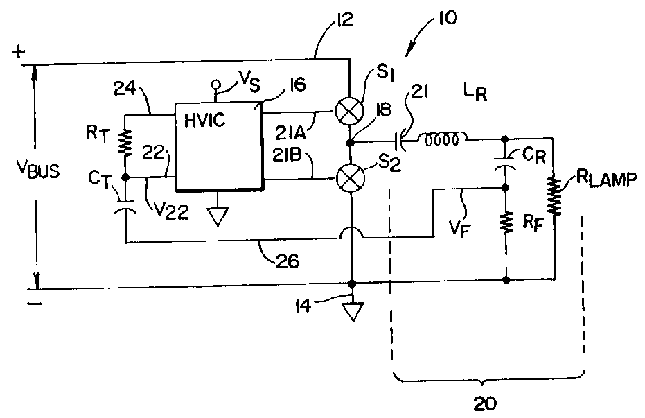
图1是气体放电灯的镇流器电路的示意图,其中一部分是以框图形式表示的。Figure 1 is a schematic diagram of a ballast circuit for a gas discharge lamp, partly shown in block diagram form.
图2表示施加到图1的高压集成电路的定时输入端的典型定时信号的电压与时间关系。FIG. 2 shows the voltage versus time of a typical timing signal applied to the timing input of the high voltage integrated circuit of FIG. 1. FIG.
图3表示触发灯和操作的稳定状态模式的操作点的简化的灯电压与角频率之间的关系。Figure 3 shows the simplified lamp voltage vs. angular frequency relationship for firing the lamp and the operating point for the steady state mode of operation.
图4表示稳定状态灯操作的定时电压和相关电压与时间的关系。Figure 4 shows timing voltages and associated voltages versus time for steady state lamp operation.
图5类似于图4,但是表示触发灯期间的电压。Figure 5 is similar to Figure 4 but shows the voltages during ignition of the lamp.
图6是向高压集成电路的定时输入端施加反馈电压的交流电路的详细的图,其中一部分是以框图形式表示的。Figure 6 is a detailed diagram, partly shown in block diagram form, of an AC circuit for applying a feedback voltage to a timing input of a high voltage integrated circuit.
图1表示对气体放电灯(例如荧光灯)供电的镇流器电路10,气体放电灯以RLAMP表示,因为它在操作期间呈现电阻特性。镇流器电路10包括一对串联的开关S1和S2,例如功率MOSFET,它们连接在总线导体12和地14之间,接收直流总线电压VBUS。通过高压集成电路(HVIC)16对开关S1和S2进行控制,这在下面详细说明。通过交替切换S1和S2,节点18交替地与总线电压VBUS和地14相连。与节点18相连的谐振负载电路20包括谐振电感LR,谐振电容CR,和灯RLAMP。电容21为负载电路20隔直。还包括了反馈电阻RF,其目的将在下面说明。由于与节点18相连,所以在谐振负载电路20中引起了交流电流。Figure 1 shows a
HVIC16可以包括带有振荡器的半桥驱动器,例如由SGS-Thompson销售的产品,产品号是L6569,名称为“带有振荡器的高压半桥驱动器”;或由加利福尼亚的EL Segundo的国际整流器公司销售的产品,产品号是IR2151,名称为“自振荡半桥驱动器”。来自HVIC16的高电压和低电压输出21A和21B驱动开关S1和S2。定时电阻RT和定时电容CT如图所示与HVIC16相连。象通常情况那样,定时电阻RT连接在电容的定时输入端22和电阻的定时输入端24之间。同时,象通常情况那样,定时电容CT的一端与电容的定时输入端22相连;然而,定时电容CT的另一端的连接不是通常的样子,这种连接与镇流器电路10中的HVIC16的反向应用有关,因此在触发灯期间在灯RLAMP的两端自动产生非常高的电压尖峰(1000-1200伏)。反馈信号,例如电压VF通过导线26送至定时电容CT的下部端子,该信号是从反馈电阻RF的上部端子引出的。相反,常规的做法是将定时电容CT的下部端子直接接地,而没有反馈电压VF到达HVIC16的定时输入端22。HVIC 16 may include a half-bridge driver with oscillator, such as that sold by SGS-Thompson, product number L6569, under the designation "High Voltage Half-Bridge Driver with Oscillator"; or by International Rectifier Corporation of EL Segundo, California The product sold, the product number is IR2151, and the name is "self-oscillating half-bridge driver". High voltage and
上述HVIC都采用定时输入端22,它接收定时信号V22,开关S1和S2的开关频率由定时信号V22从一个阈值到另一个阈值或从另一个阈值到一个阈值的各个过渡时间确定。参看图2,可能的定时信号V22在一对阈值电压之间变化,如图所示,这对阈值电压可以是提供给图1的HVIC的电源电压Vs和2/3Vs。一般来说,当定时信号V22从较低的阈值增加,并达到较高的阈值时,定时电阻RT的上部端子变成与地26相连,因此定时信号V22通过定时电阻放电。类似地,定时信号V22变为较低的阈值时,定时电阻RT的上部端子与电源Vs相连,使定时信号V22向着较高阈值增加。在过渡点,例如在图2中的时刻t1、t2、t3和t4,使开关S1和S2交替切换。The above HVICs all use
在触发灯之前,灯RLAMP呈现极高的电阻。在这段时间,谐振负载电路20的Q值或品质因数非常高,因为灯对电路不增加显著(即低)的电阻负载。这时,控制开关S1和S2是非常有利的,因此谐振负载电路20的操作频率到达其固有谐振点。当出现这种情况时,灯两端的电压具有非常高的尖峰,这是触发灯所需要的。The lamp R LAMP presents a very high resistance until the lamp is triggered. During this time, the Q or quality factor of the resonated
图3表示灯电压与角频率的简化的图,用以说明灯触发和稳定状态模式之间的操作。灯电压以分贝测量,角频率以弧度测量。在角频率ε2,稳定状态操作点是30,稳定状态电压是Vss。角频率降低到ε1,灯电压升高到VIGNITION,这对触发灯来说是足够的。触发灯以后,灯呈现低得多的阻抗,使谐振负载电路20的Q值降低,因此导致较低的稳定状态电压Vss。Figure 3 shows a simplified plot of lamp voltage versus angular frequency to illustrate operation between lamp ignition and steady state modes. Lamp voltage is measured in decibels and angular frequency is measured in radians. At angular frequency ε2, the steady-state operating point is 30, and the steady-state voltage is Vss. The angular frequency decreases to ε1 and the lamp voltage increases to V IGNITION , which is sufficient to ignite the lamp. After firing the lamp, the lamp presents a much lower impedance, reducing the Q of the
通过向HVIC16的定时输入端22施加反馈信号VF,在触发灯期间将出现所要求的角频率偏移,得到触发灯所需的非常高的电压尖峰。图2表示定时信号V22,它是基本对称的上、下指数变化的形式,与上述HVIC16的定时输入端22按常规方法连接具有相同的时间常数。这导致灯操作的固定频率,这将适合于稳定状态的灯操作。HVIC16的定时输入端22上的定时电压V22构成了当定时电容CT充电或放电时的电压以及反馈信号VF的电压之和。在稳定状态灯操作期间,反馈电压VF相对于定时电容CT充电或放电时的电压来说相当小。于是,在稳定状态灯操作期间,定时电压V22主要由定时电容CT充电或放电确定。(然而在其它实施利中,定时电压主要由稳定状态灯操作期间的反馈电压控制。)图4表示产生定时电压V22的电压之和。By applying feedback signal VF to timing
在图4中,实线表示定时电压V22。长虚线32表示定时电容CT的充电电压。短虚线VF表示非常小的反馈信号。于是,定时电压V22主要由稳定状态操作期间电容CT的充电确定。图5表示在触发灯期间这些电压的情况。In FIG. 4, the solid line represents the timing voltage V22. The long
参照图5,本发明的优点是当谐振负载电路20基本上没有灯作为负载时(即此时灯不具有低的电阻),在触发灯期间谐振负载电路20中存在相当高的电压(和电流)。因此,在触发灯期间,反馈信号VF将远远高于稳定状态灯操作期间的反馈信号VF。曲线32表示定时电容CT的充电情况,这与图4的稳定状态的情况相似,图5中定时电压V22没有升高得那样快。其理由是,在HVIC16的定时输入端22,定时电容CT的电压与反馈电压VF的反相值相加。然而图中反馈电压VF不是以其反向值表示的。将反馈电压VF的反相值与曲线32相加得到上述相当低的定时电压V22。结果,如以上结合附图2所示讨论的那样,定时电压V22从一个阈值到另一个阈值的过渡时间增加了。从图2可以清楚地看到,HVIC16的操作频率降低了。频率的这种降低是从图3所示的稳定状态操作频率ε2变到ε1的谐振负载电路20的固有谐振频率。这导致触发灯所需的非常高的灯电压尖峰。然而,一旦灯被触发,谐振负载电路中的反馈电压VF和其它电压的幅度急剧下降,于是如上面结合图4所描述的那样,反馈电压VF对定时电压V22的影响可忽视。5, an advantage of the present invention is that when the
对一个20瓦的灯来说,总线电压VBUS是170伏,图1所示的镇流器电路10的部件的典型值如下:谐振电感LR是800微亨;谐振电容CR是5.6毫微法;反馈电阻RF是3.3欧姆;隔直电容21是0.22微法;定时电阻RT是10.5千欧姆,定时电容CT是0.001微法。For a 20 watt lamp, the bus voltage V BUS is 170 volts. Typical values for the components of the
图6表示向定时输入端22施加反馈电压VF的另一电路。如图所示,通过反馈定时电容CT2向HVIC16的定时输入端22施加反馈电压VF。定时电容CT的下部端子直接与地14相连。在本实施例中,反馈电压VF与定时输入端22容性耦合,并在该输入端与定时电容CT两端的电压相加。最后得到的镇流器电路的作用与以上结合图1所描述的类似。更具体地说,在触发灯期间建立定时电压V22时,反馈电压VF占主导地位,而在稳定状态灯操作期间,定时电容CT两端的电压占主导地位。FIG. 6 shows another circuit for applying the feedback voltage V F to the
如上所述,本发明的实施例可以使在建立定时电压V22时,在触发灯期间和稳定状态操作期间反馈电压VF都占主导地位。例如,可以增加反馈电阻RF的阻值,以便提高其两端的反馈电压VF。与图4所示的可忽视的反馈电压VF相反,在稳定状态操作期间反馈电压VF变得非常大。As described above, embodiments of the present invention allow the feedback voltage VF to dominate both during lamp ignition and during steady state operation in establishing timing voltage V22. For example, the resistance value of the feedback resistor R F can be increased to increase the feedback voltage V F across it. In contrast to the negligible feedback voltage V F shown in FIG. 4 , the feedback voltage V F becomes very large during steady state operation.
虽然以上结合本发明的具体实施例进行了描述,但是对本领域的一般技术人员来说,在不脱离本发明的精神和范围的前提下,可进行各种修改和改进。Although the specific embodiments of the present invention have been described above, those skilled in the art can make various modifications and improvements without departing from the spirit and scope of the present invention.
Claims (17)
Applications Claiming Priority (2)
| Application Number | Priority Date | Filing Date | Title |
|---|---|---|---|
| US08/648,232 US5719472A (en) | 1996-05-13 | 1996-05-13 | High voltage IC-driven half-bridge gas discharge ballast |
| US648,232 | 1996-05-13 |
Publications (1)
| Publication Number | Publication Date |
|---|---|
| CN1180986A true CN1180986A (en) | 1998-05-06 |
Family
ID=24599956
Family Applications (1)
| Application Number | Title | Priority Date | Filing Date |
|---|---|---|---|
| CN97111591A Pending CN1180986A (en) | 1996-05-13 | 1997-05-13 | High-voltage IC driving half-bridge gas discharge lamp ballast |
Country Status (4)
| Country | Link |
|---|---|
| US (1) | US5719472A (en) |
| EP (1) | EP0808086A1 (en) |
| JP (1) | JPH1055893A (en) |
| CN (1) | CN1180986A (en) |
Families Citing this family (14)
| Publication number | Priority date | Publication date | Assignee | Title |
|---|---|---|---|---|
| US6008593A (en) * | 1997-02-12 | 1999-12-28 | International Rectifier Corporation | Closed-loop/dimming ballast controller integrated circuits |
| JP2972691B2 (en) * | 1997-02-12 | 1999-11-08 | インターナショナル・レクチファイヤー・コーポレーション | Phase control circuit for electronic ballast |
| US6300777B1 (en) | 1997-10-15 | 2001-10-09 | International Rectifier Corporation | Lamp ignition detection circuit |
| US6008592A (en) * | 1998-06-10 | 1999-12-28 | International Rectifier Corporation | End of lamp life or false lamp detection circuit for an electronic ballast |
| US6495971B1 (en) | 1998-06-13 | 2002-12-17 | Hatch Transformers, Inc. | High intensity discharge lamp ballast |
| US6188183B1 (en) | 1998-06-13 | 2001-02-13 | Simon Richard Greenwood | High intensity discharge lamp ballast |
| DE19912981C1 (en) * | 1999-03-22 | 2000-12-21 | Univ Magdeburg Tech | Supply of a wide range of plasmas e.g. for use in biological processes by supplying a barrier discharge using sequentially adjustable phases |
| US6198226B1 (en) * | 1999-08-18 | 2001-03-06 | Astronics Corporation | Low-noise drive circuit for electroluminescent lamp, and electroluminescent lamp assembly comprising same |
| US6906473B2 (en) * | 2003-08-26 | 2005-06-14 | Osram Sylvania Inc. | Feedback circuit and method of operating ballast resonant inverter |
| US7030570B2 (en) * | 2004-07-07 | 2006-04-18 | Osram Sylvania Inc. | Resonant inverter including feed back circuit with source of variable bias current |
| US7045966B2 (en) | 2004-07-07 | 2006-05-16 | Osram Sylvania Inc. | Resonant inverter including feed back circuit having phase compensator and controller |
| US7095183B2 (en) | 2004-07-07 | 2006-08-22 | Osram Sylvania Inc. | Control system for a resonant inverter with a self-oscillating driver |
| US7589480B2 (en) * | 2006-05-26 | 2009-09-15 | Greenwood Soar Ip Ltd. | High intensity discharge lamp ballast |
| GB201502453D0 (en) | 2015-02-13 | 2015-04-01 | Spts Technologies Ltd | Plasma producing apparatus |
Family Cites Families (13)
| Publication number | Priority date | Publication date | Assignee | Title |
|---|---|---|---|---|
| US4585974A (en) * | 1983-01-03 | 1986-04-29 | North American Philips Corporation | Varible frequency current control device for discharge lamps |
| US4791338A (en) * | 1986-06-26 | 1988-12-13 | Thomas Industries, Inc. | Fluorescent lamp circuit with regulation responsive to voltage, current, and phase of load |
| US4952849A (en) * | 1988-07-15 | 1990-08-28 | North American Philips Corporation | Fluorescent lamp controllers |
| EP0359860A1 (en) * | 1988-09-23 | 1990-03-28 | Siemens Aktiengesellschaft | Device and method for operating at least one discharge lamp |
| US5075599A (en) * | 1989-11-29 | 1991-12-24 | U.S. Philips Corporation | Circuit arrangement |
| DE4018865A1 (en) * | 1990-01-20 | 1991-12-19 | Semperlux Gmbh | ELECTRONIC CONTROL UNIT FOR THE OPERATION OF DISCHARGE LAMPS |
| US5051662A (en) * | 1990-03-27 | 1991-09-24 | Usi Lighting, Inc. | Fluorescent lamp system |
| US5408162A (en) * | 1992-03-26 | 1995-04-18 | Linear Technology Corporation | Fluorescent lamp power supply and control unit |
| US5382881A (en) * | 1992-12-28 | 1995-01-17 | North American Philips Corporation | Ballast stabilization circuitry for eliminating moding or oscillation of the current envelope in gas discharge lamps and method of operating |
| US5382882A (en) * | 1993-04-20 | 1995-01-17 | General Electric Company | Power supply circuit for a gas discharge lamp |
| US5406177A (en) * | 1994-04-18 | 1995-04-11 | General Electric Company | Gas discharge lamp ballast circuit with compact starting circuit |
| US5619104A (en) * | 1994-10-07 | 1997-04-08 | Samsung Electronics Co., Ltd. | Multiplier that multiplies the output voltage from the control circuit with the voltage from the boost circuit |
| US5612597A (en) * | 1994-12-29 | 1997-03-18 | International Rectifier Corporation | Oscillating driver circuit with power factor correction, electronic lamp ballast employing same and driver method |
-
1996
- 1996-05-13 US US08/648,232 patent/US5719472A/en not_active Expired - Fee Related
-
1997
- 1997-05-09 JP JP9118536A patent/JPH1055893A/en not_active Withdrawn
- 1997-05-13 EP EP97303238A patent/EP0808086A1/en not_active Withdrawn
- 1997-05-13 CN CN97111591A patent/CN1180986A/en active Pending
Also Published As
| Publication number | Publication date |
|---|---|
| JPH1055893A (en) | 1998-02-24 |
| EP0808086A1 (en) | 1997-11-19 |
| US5719472A (en) | 1998-02-17 |
Similar Documents
| Publication | Publication Date | Title |
|---|---|---|
| US6518712B2 (en) | Method and apparatus for controlling the operation of a lamp | |
| US5751120A (en) | DC operated electronic ballast for fluorescent light | |
| CN1251558C (en) | Integrated circuit for lamp heating and dimming control | |
| US6127786A (en) | Ballast having a lamp end of life circuit | |
| US6348769B1 (en) | Electronic ballast | |
| EP1128709B1 (en) | Power regulation circuit for ballast for ceramic metal halide lamp | |
| CN1180986A (en) | High-voltage IC driving half-bridge gas discharge lamp ballast | |
| JP2002516020A (en) | Power supply device for power supply and lighting of discharge lamp | |
| US5723953A (en) | High voltage IC-driven half-bridge gas discharge lamp ballast | |
| CN1293531A (en) | Electrodless fluorescent lamp light regulating system | |
| EP0502512B1 (en) | Starting and operating circuit for arc discharge lamp | |
| EP0772956A1 (en) | Circuit arrangement | |
| US6157142A (en) | Hid ballast circuit with arc stabilization | |
| WO2000045622A1 (en) | Hid ballast with hot restart circuit | |
| JP2001338789A (en) | Discharge lamp lighting device | |
| US7164239B2 (en) | Discharge lamp ballast circuit | |
| US7397196B2 (en) | Circuit arrangement for preventing high peak currents | |
| CN1179077A (en) | High-voltage integrated circuit driving half-bridge gas discharge lamp ballast | |
| JP4179173B2 (en) | Discharge lamp lighting device, lighting device, projector | |
| JP3125459B2 (en) | Discharge lamp lighting device | |
| JP4398180B2 (en) | Discharge lamp driving device | |
| JP2000215992A (en) | Discharge lamp lighting device | |
| JPH1126180A (en) | Discharge lamp lighting device | |
| JP2002015889A (en) | High-pressure discharge lamp lighting device | |
| JP2000058282A (en) | Discharge lamp lighting device |
Legal Events
| Date | Code | Title | Description |
|---|---|---|---|
| C06 | Publication | ||
| PB01 | Publication | ||
| C10 | Entry into substantive examination | ||
| SE01 | Entry into force of request for substantive examination | ||
| C02 | Deemed withdrawal of patent application after publication (patent law 2001) | ||
| WD01 | Invention patent application deemed withdrawn after publication |