CN1237496C - display device - Google Patents
display device Download PDFInfo
- Publication number
- CN1237496C CN1237496C CNB998016756A CN99801675A CN1237496C CN 1237496 C CN1237496 C CN 1237496C CN B998016756 A CNB998016756 A CN B998016756A CN 99801675 A CN99801675 A CN 99801675A CN 1237496 C CN1237496 C CN 1237496C
- Authority
- CN
- China
- Prior art keywords
- light
- display device
- mentioned
- light source
- color
- Prior art date
- Legal status (The legal status is an assumption and is not a legal conclusion. Google has not performed a legal analysis and makes no representation as to the accuracy of the status listed.)
- Expired - Lifetime
Links
Images


Classifications
-
- G—PHYSICS
- G02—OPTICS
- G02F—OPTICAL DEVICES OR ARRANGEMENTS FOR THE CONTROL OF LIGHT BY MODIFICATION OF THE OPTICAL PROPERTIES OF THE MEDIA OF THE ELEMENTS INVOLVED THEREIN; NON-LINEAR OPTICS; FREQUENCY-CHANGING OF LIGHT; OPTICAL LOGIC ELEMENTS; OPTICAL ANALOGUE/DIGITAL CONVERTERS
- G02F1/00—Devices or arrangements for the control of the intensity, colour, phase, polarisation or direction of light arriving from an independent light source, e.g. switching, gating or modulating; Non-linear optics
- G02F1/01—Devices or arrangements for the control of the intensity, colour, phase, polarisation or direction of light arriving from an independent light source, e.g. switching, gating or modulating; Non-linear optics for the control of the intensity, phase, polarisation or colour
- G02F1/13—Devices or arrangements for the control of the intensity, colour, phase, polarisation or direction of light arriving from an independent light source, e.g. switching, gating or modulating; Non-linear optics for the control of the intensity, phase, polarisation or colour based on liquid crystals, e.g. single liquid crystal display cells
- G02F1/133—Constructional arrangements; Operation of liquid crystal cells; Circuit arrangements
- G02F1/1333—Constructional arrangements; Manufacturing methods
- G02F1/1335—Structural association of cells with optical devices, e.g. polarisers or reflectors
- G02F1/1336—Illuminating devices
- G02F1/133621—Illuminating devices providing coloured light
-
- G—PHYSICS
- G09—EDUCATION; CRYPTOGRAPHY; DISPLAY; ADVERTISING; SEALS
- G09F—DISPLAYING; ADVERTISING; SIGNS; LABELS OR NAME-PLATES; SEALS
- G09F9/00—Indicating arrangements for variable information in which the information is built-up on a support by selection or combination of individual elements
-
- G—PHYSICS
- G02—OPTICS
- G02F—OPTICAL DEVICES OR ARRANGEMENTS FOR THE CONTROL OF LIGHT BY MODIFICATION OF THE OPTICAL PROPERTIES OF THE MEDIA OF THE ELEMENTS INVOLVED THEREIN; NON-LINEAR OPTICS; FREQUENCY-CHANGING OF LIGHT; OPTICAL LOGIC ELEMENTS; OPTICAL ANALOGUE/DIGITAL CONVERTERS
- G02F1/00—Devices or arrangements for the control of the intensity, colour, phase, polarisation or direction of light arriving from an independent light source, e.g. switching, gating or modulating; Non-linear optics
- G02F1/01—Devices or arrangements for the control of the intensity, colour, phase, polarisation or direction of light arriving from an independent light source, e.g. switching, gating or modulating; Non-linear optics for the control of the intensity, phase, polarisation or colour
- G02F1/13—Devices or arrangements for the control of the intensity, colour, phase, polarisation or direction of light arriving from an independent light source, e.g. switching, gating or modulating; Non-linear optics for the control of the intensity, phase, polarisation or colour based on liquid crystals, e.g. single liquid crystal display cells
- G02F1/133—Constructional arrangements; Operation of liquid crystal cells; Circuit arrangements
- G02F1/1333—Constructional arrangements; Manufacturing methods
- G02F1/1335—Structural association of cells with optical devices, e.g. polarisers or reflectors
- G02F1/1336—Illuminating devices
- G02F1/133602—Direct backlight
- G02F1/133603—Direct backlight with LEDs
-
- G—PHYSICS
- G02—OPTICS
- G02F—OPTICAL DEVICES OR ARRANGEMENTS FOR THE CONTROL OF LIGHT BY MODIFICATION OF THE OPTICAL PROPERTIES OF THE MEDIA OF THE ELEMENTS INVOLVED THEREIN; NON-LINEAR OPTICS; FREQUENCY-CHANGING OF LIGHT; OPTICAL LOGIC ELEMENTS; OPTICAL ANALOGUE/DIGITAL CONVERTERS
- G02F1/00—Devices or arrangements for the control of the intensity, colour, phase, polarisation or direction of light arriving from an independent light source, e.g. switching, gating or modulating; Non-linear optics
- G02F1/01—Devices or arrangements for the control of the intensity, colour, phase, polarisation or direction of light arriving from an independent light source, e.g. switching, gating or modulating; Non-linear optics for the control of the intensity, phase, polarisation or colour
- G02F1/13—Devices or arrangements for the control of the intensity, colour, phase, polarisation or direction of light arriving from an independent light source, e.g. switching, gating or modulating; Non-linear optics for the control of the intensity, phase, polarisation or colour based on liquid crystals, e.g. single liquid crystal display cells
- G02F1/133—Constructional arrangements; Operation of liquid crystal cells; Circuit arrangements
- G02F1/1333—Constructional arrangements; Manufacturing methods
- G02F1/1335—Structural association of cells with optical devices, e.g. polarisers or reflectors
- G02F1/1336—Illuminating devices
- G02F1/133621—Illuminating devices providing coloured light
- G02F1/133622—Colour sequential illumination
-
- G—PHYSICS
- G09—EDUCATION; CRYPTOGRAPHY; DISPLAY; ADVERTISING; SEALS
- G09G—ARRANGEMENTS OR CIRCUITS FOR CONTROL OF INDICATING DEVICES USING STATIC MEANS TO PRESENT VARIABLE INFORMATION
- G09G2310/00—Command of the display device
- G09G2310/02—Addressing, scanning or driving the display screen or processing steps related thereto
- G09G2310/0235—Field-sequential colour display
-
- G—PHYSICS
- G09—EDUCATION; CRYPTOGRAPHY; DISPLAY; ADVERTISING; SEALS
- G09G—ARRANGEMENTS OR CIRCUITS FOR CONTROL OF INDICATING DEVICES USING STATIC MEANS TO PRESENT VARIABLE INFORMATION
- G09G3/00—Control arrangements or circuits, of interest only in connection with visual indicators other than cathode-ray tubes
- G09G3/20—Control arrangements or circuits, of interest only in connection with visual indicators other than cathode-ray tubes for presentation of an assembly of a number of characters, e.g. a page, by composing the assembly by combination of individual elements arranged in a matrix no fixed position being assigned to or needed to be assigned to the individual characters or partial characters
- G09G3/34—Control arrangements or circuits, of interest only in connection with visual indicators other than cathode-ray tubes for presentation of an assembly of a number of characters, e.g. a page, by composing the assembly by combination of individual elements arranged in a matrix no fixed position being assigned to or needed to be assigned to the individual characters or partial characters by control of light from an independent source
- G09G3/3406—Control of illumination source
- G09G3/3413—Details of control of colour illumination sources
-
- H—ELECTRICITY
- H10—SEMICONDUCTOR DEVICES; ELECTRIC SOLID-STATE DEVICES NOT OTHERWISE PROVIDED FOR
- H10K—ORGANIC ELECTRIC SOLID-STATE DEVICES
- H10K50/00—Organic light-emitting devices
- H10K50/80—Constructional details
- H10K50/868—Arrangements for polarized light emission
-
- H—ELECTRICITY
- H10—SEMICONDUCTOR DEVICES; ELECTRIC SOLID-STATE DEVICES NOT OTHERWISE PROVIDED FOR
- H10K—ORGANIC ELECTRIC SOLID-STATE DEVICES
- H10K59/00—Integrated devices, or assemblies of multiple devices, comprising at least one organic light-emitting element covered by group H10K50/00
- H10K59/30—Devices specially adapted for multicolour light emission
- H10K59/35—Devices specially adapted for multicolour light emission comprising red-green-blue [RGB] subpixels
- H10K59/352—Devices specially adapted for multicolour light emission comprising red-green-blue [RGB] subpixels the areas of the RGB subpixels being different
-
- H—ELECTRICITY
- H10—SEMICONDUCTOR DEVICES; ELECTRIC SOLID-STATE DEVICES NOT OTHERWISE PROVIDED FOR
- H10K—ORGANIC ELECTRIC SOLID-STATE DEVICES
- H10K59/00—Integrated devices, or assemblies of multiple devices, comprising at least one organic light-emitting element covered by group H10K50/00
- H10K59/30—Devices specially adapted for multicolour light emission
- H10K59/35—Devices specially adapted for multicolour light emission comprising red-green-blue [RGB] subpixels
- H10K59/353—Devices specially adapted for multicolour light emission comprising red-green-blue [RGB] subpixels characterised by the geometrical arrangement of the RGB subpixels
-
- H—ELECTRICITY
- H10—SEMICONDUCTOR DEVICES; ELECTRIC SOLID-STATE DEVICES NOT OTHERWISE PROVIDED FOR
- H10K—ORGANIC ELECTRIC SOLID-STATE DEVICES
- H10K59/00—Integrated devices, or assemblies of multiple devices, comprising at least one organic light-emitting element covered by group H10K50/00
- H10K59/80—Constructional details
- H10K59/8791—Arrangements for improving contrast, e.g. preventing reflection of ambient light
-
- H—ELECTRICITY
- H10—SEMICONDUCTOR DEVICES; ELECTRIC SOLID-STATE DEVICES NOT OTHERWISE PROVIDED FOR
- H10K—ORGANIC ELECTRIC SOLID-STATE DEVICES
- H10K59/00—Integrated devices, or assemblies of multiple devices, comprising at least one organic light-emitting element covered by group H10K50/00
- H10K59/80—Constructional details
- H10K59/8793—Arrangements for polarized light emission
Landscapes
- Physics & Mathematics (AREA)
- Nonlinear Science (AREA)
- General Physics & Mathematics (AREA)
- Optics & Photonics (AREA)
- Mathematical Physics (AREA)
- Chemical & Material Sciences (AREA)
- Crystallography & Structural Chemistry (AREA)
- Theoretical Computer Science (AREA)
- Engineering & Computer Science (AREA)
- Liquid Crystal (AREA)
- Electroluminescent Light Sources (AREA)
- Devices For Indicating Variable Information By Combining Individual Elements (AREA)
- Illuminated Signs And Luminous Advertising (AREA)
- Electric Clocks (AREA)
Abstract
Description
技术领域technical field
本发明涉及在计算机、电视机及携带电话机等信息装置终端的显示器中使用的显示装置,以及在显示装置中使用的背照光源的结构。The present invention relates to a display device used in displays of information device terminals such as computers, televisions, and mobile phones, and to a structure of a backlight used in the display device.
背景技术Background technique
例如,在使用现有液晶的彩色显示装置中,与彩色CRT相同,把一个像素分割成对应于红绿蓝各色的色像素,同时,形成与各个色像素对应的彩色滤光片,以白色背照光源从背面进行照明,同时显示各个色,来显示一个像素的颜色。但是,在该方法中存在着下述问题,由于对一个像素进行三分割,故像素的孔径值降低且显示变暗,驱动液晶面板用的信号驱动器的个数需要与各色对应的数目,此外,需要与色像素同样细度的彩色滤光片,而且,成本变高等。For example, in a color display device using a conventional liquid crystal, like a color CRT, one pixel is divided into color pixels corresponding to red, green, and blue colors, and at the same time, color filters corresponding to each color pixel are formed, and a white background color is used. The light source illuminates from the back and displays each color at the same time to display the color of one pixel. However, this method has the following problems. Since one pixel is divided into three, the aperture value of the pixel decreases and the display becomes dark, and the number of signal drivers for driving the liquid crystal panel needs to be the number corresponding to each color. In addition, A color filter having the same fineness as a color pixel is required, and the cost becomes higher.
因此,正如特开平5-19257中所示,提出了把多色背景光源与光阀组合起来的彩色显示装置。按照该结构,不把一个像素分割成红绿蓝各色,因此,例如在使用有源矩阵面板的情况下,具有下述优点,由于整个面板应该形成的有源元件的个数成为三分之一,故成品率提高了,提高了一个像素的孔径值且显示变亮、信号驱动器的个数成为现有的三分之一,此外,不需要彩色滤光片,所以,成本降低了等。Therefore, as shown in JP-A-5-19257, a color display device combining a multi-color background light source and a light valve has been proposed. According to this configuration, one pixel is not divided into red, green, and blue colors. Therefore, for example, in the case of using an active matrix panel, there is an advantage that the number of active elements that should be formed on the entire panel is reduced by one-third. , so the yield is improved, the aperture value of one pixel is increased and the display becomes brighter, and the number of signal drivers becomes one-third of the existing number. In addition, no color filter is required, so the cost is reduced.
在使用冷阴极管的结构中,在特开平5-19257中,公开了有关其配置显示出了RGB各自的冷阴极管及与其对置的导光板的层叠结构,此外,还示出了有关驱动方法。在特开平5-264988及特开平5-346570中,示出了在一块导光板的一个端面上并排配置RGB这三个冷阴极管的结构,以及利用RGB滤光光阀把来自一个白色发光体的光变换成时分割RGB光的结构。在特开平6-67149中,示出了把RGB这三个冷阴极管配置在面板背面的结构及其驱动方法。特别是,独立地调整对各色背照光源的供给电压,以便取得彩色平衡。在特开平6-301004中,作为RGB转换的背照光源,公开了白色光源、RGB彩色滤光片、液晶光阀与扩散板的组合。在特开平6-301032中,公开了RGB光源与液晶光阀的组合。此外,在特开平9-101497中,公开了利用TN模式液晶光阀及上述结构进行灰度显示用的驱动方法。在特开平9-114421中,在使用了TFT元件的结构中,在改写图像信号时,对液晶的状态进行复位,由此,可得到鲜明的显示。In the structure using cold cathode tubes, Japanese Unexamined Patent Publication No. 5-19257 discloses the configuration showing the laminated structure of each RGB cold cathode tube and the light guide plate facing it. In addition, it also shows the driving method. In JP-A-5-264988 and JP-A-5-346570, it is shown that three cold-cathode tubes of RGB are arranged side by side on one end surface of a light guide plate, and the RGB light filter valve is used to transfer light from a white luminous body. The light is transformed into a time-segmented RGB light structure. JP-A-6-67149 discloses a structure in which three cold-cathode tubes of RGB are arranged on the back of a panel and a driving method thereof. In particular, the supply voltages to the backlights of each color are independently adjusted in order to achieve color balance. JP-A-6-301004 discloses a combination of a white light source, an RGB color filter, a liquid crystal light valve, and a diffuser plate as an RGB conversion backlight. JP-A-6-301032 discloses a combination of an RGB light source and a liquid crystal light valve. Furthermore, JP-A-9-101497 discloses a driving method for gradation display using a TN-mode liquid crystal light valve and the above structure. In Japanese Unexamined Patent Publication No. 9-114421, in the structure using the TFT element, when rewriting an image signal, the state of the liquid crystal is reset, whereby a clear display can be obtained.
另一方面,正如特开平3-187192中所示,作为现有的直观型彩色显示装置的背照光源,还公开了使用作为薄型低功耗的有机EL的光源。On the other hand, as shown in Japanese Unexamined Patent Publication No. 3-187192, a light source using an organic EL, which is thin and low in power consumption, is also disclosed as a backlight source for a conventional direct-view type color display device.
在上述那样的现有技术中,在作为多色背照光源使用了冷阴极管等光源的情况下,存在着下述问题,由于驱动电路是复杂的,故外形大且成本高,背照光源的耗电大,不能用于携带型信息装置中等。In the prior art as above, when a light source such as a cold-cathode tube is used as a multi-color backlight source, there are following problems. The drive circuit is complicated, so the appearance is large and the cost is high. It consumes a lot of power and cannot be used in portable information devices.
此外,在背照光源中使用了有机EL的特开平3-187192中,由于只是配置了RGB的EL元件来代替现有彩色液晶面板的彩色滤光片,故需要与现有同等的像素个数,驱动器的个数也与现有的同等。因而,成本还是高,孔径值还是低。In addition, in Japanese Patent Laid-Open No. 3-187192, which uses organic EL as a backlight, only RGB EL elements are arranged instead of the color filters of conventional color liquid crystal panels, so the same number of pixels as conventional ones is required. , the number of drives is also the same as the existing ones. Therefore, the cost is still high, and the aperture value is still low.
发明的公开disclosure of invention
本发明是鉴于上述问题而进行的,其课题在于,提供结构简单,驱动电路也简单的多色光源,进而提供使用了该光源的,紧凑的,低功耗,而且低成本的显示装置。The present invention has been made in view of the above problems, and an object of the present invention is to provide a multi-color light source with a simple structure and a simple driving circuit, and to provide a compact, low-power, and low-cost display device using the light source.
本发明的显示装置的特征在于,具备:The display device of the present invention is characterized in that it has:
平面型光调制面板;以及a planar light modulating panel; and
面状光源,该面状光源被配置到该平面型光调制面板的背面一侧,在实际上与该平面型光调制面板的平面行的面内至少具有:具备以第一色进行发光的发光材料的第1发光区;以及具备以与该第1色不同的第2色进行发光的发光材料的第2发光区,A planar light source, which is arranged on the back side of the planar light modulation panel, and has at least: a light emitting light emitting in a first color in a plane parallel to the plane of the planar light modulation panel. a first light-emitting region of a material; and a second light-emitting region comprising a light-emitting material that emits light in a second color different from the first color,
把进行显示的彩色图像的一段扫描时间分割成该面状光源的发光颜色的个数,对应于已分割的各个期间,使各发光区发光,利用平面型光调制面板来形成与该期间同步地进行发光的发光色的亮度信息,利用该面板对各色光进行光调制,进行彩色显示。Divide a period of scanning time of the displayed color image into the number of luminous colors of the planar light source, make each luminous region emit light corresponding to each divided period, and use a planar light modulation panel to form a synchronous pattern with the period. The brightness information of the luminescent color that emits light is used to perform light modulation for each color light using the panel to perform color display.
再有,按照本发明可提供下述显示装置,其特征在于,具备:Furthermore, according to the present invention, the following display device can be provided, which is characterized in that:
平面型光调制面板;以及a planar light modulating panel; and
面状光源,该面状光源至少具有配置到该平面型光调制面板的背面一侧,在实际上与该平面型光调制面板的面平行的面内至少具有:具备以第1色的波长区进行发光的发光材料的第1发光区;以及具备以与该第1色不同的第2色的波长区进行发光的发光材料的第2发光区,该第1发光区及第2发光区分别具有螺旋状的形状。A planar light source having at least one side disposed on the back side of the planar light modulation panel, and having at least: a wavelength region with a first color in a plane substantially parallel to the plane of the planar light modulation panel A first light-emitting region of a light-emitting material that emits light; and a second light-emitting region with a light-emitting material that emits light in a wavelength region of a second color different from the first color, the first light-emitting region and the second light-emitting region respectively have Spiral shape.
附图的简单说明A brief description of the drawings
图1为示出实施例1的显示装置光源部的结构的平面图;1 is a plan view showing the structure of a light source portion of a display device according to Embodiment 1;
图2为示出实施例1的显示装置剖面结构及连接的图;Fig. 2 is the figure showing the sectional structure and connection of the display device of embodiment 1;
图3为示出在驱动实施例1的显示装置时的光源的驱动波形及伴随着该波形的光源输出和光调制面板的透射率的图;3 is a graph showing a driving waveform of a light source when driving the display device of Embodiment 1, and a light source output accompanying the waveform and a transmittance of a light modulation panel;
图4为示出实施例2的显示装置光源部的结构的平面图;4 is a plan view showing the structure of a light source portion of a display device according to Embodiment 2;
图5为示出在驱动实施例2的显示装置时的光源的驱动波形及伴随着该波形的光源输出的光调制面板的透射率的图;5 is a graph showing a driving waveform of a light source when driving the display device of Example 2 and the transmittance of the light modulation panel accompanying the waveform of the light source output;
图6为示出实施例3的显示装置光源部的结构的平面图;6 is a plan view showing the structure of a light source portion of a display device according to Embodiment 3;
图7为示出实施例4的显示装置剖面结构及连接的图;7 is a diagram showing a cross-sectional structure and connections of a display device in Embodiment 4;
图8为示出实施例5的显示装置剖面结构及连接的图;8 is a diagram showing a cross-sectional structure and connection of a display device in Embodiment 5;
图9为示出实施例6的显示装置剖面结构及连接的图;9 is a diagram showing a cross-sectional structure and connections of a display device in Embodiment 6;
图10为示出实施例7的显示装置制造工艺的剖面图;10 is a cross-sectional view showing the manufacturing process of the display device of Embodiment 7;
图11为示出实施例8的显示装置剖面结构及连接的图;11 is a diagram showing a cross-sectional structure and connections of a display device in Embodiment 8;
图12为示出实施例10的的显示装置的剖面及连接的图;12 is a diagram showing a cross section and connections of a display device in
图13为示出实施例11的显示装置的结构的剖面图;13 is a cross-sectional view showing the structure of a display device of Embodiment 11;
图14为示出实施例12的显示装置剖面结构及连接的图;14 is a diagram showing a cross-sectional structure and connections of a display device in Embodiment 12;
图15为示出实施例14中的面状光源发光区的图形形状的平面图;以及Fig. 15 is a plan view showing the figure shape of the light emitting area of the planar light source in Embodiment 14; and
图16为示出实施例15中的面状光源发光区的图形形状的平面图。FIG. 16 is a plan view showing the pattern shape of the light-emitting area of the planar light source in Embodiment 15. FIG.
实施发明用的最佳形态Optimum Form for Carrying Out the Invention
本发明的显示装置是具有把能够发多色光的面状光源与平面型光调制面板重叠起来的结构,对该光调制面板进行扫描,形成彩色图像的显示装置,其中,把彩色图像的一段扫描时间分割成与光源的发光颜色的个数相同的个数,点亮对应于已分割的各个期间(色显示期间)的色的光源,通过与此同步地在平面型光调制面板上显示该色的亮度信息来进行彩色显示。而且,面状光源的特征在于下述各点:被配置到该平面型光调制面板的背面一侧,在实际上与该光阀的平行的面内至少具有:具备以第1色进行发光的发光材料、即把第1色的波长区作为发光波长的发光材料的第1发光区;以及具备以与该第1色不同的第2色进行发光的发光材料、即把第2色的波长区作为发光波长的发光材料的第2发光区,进行多色的发光,把进行显示的彩色图像的一段扫描时间分割成该面状光源的发光颜色的个数,具体地说,是发光区种类的个数,进行图像显示。The display device of the present invention is a display device in which a planar light source capable of emitting polychromatic light and a planar light modulation panel are superimposed, and the light modulation panel is scanned to form a color image, wherein a section of the color image is scanned Time is divided into the same number as the number of light emitting colors of the light sources, light sources of colors corresponding to the divided periods (color display periods) are turned on, and the color is displayed on the flat light modulation panel in synchronization with this. Brightness information for color display. Furthermore, the planar light source is characterized in that it is disposed on the rear side of the planar light modulation panel, and has at least a light source that emits light in a first color in a plane substantially parallel to the light valve. A luminescent material, that is, the first luminescent region of the luminescent material that uses the wavelength region of the first color as the emission wavelength; and a luminescent material that emits light in a second color different from the first color, that is, the wavelength region of the second color As the second luminous region of the luminescent material of the luminescent wavelength, multi-color luminescence is performed, and a scanning time of the displayed color image is divided into the number of luminescent colors of the planar light source, specifically, the type of the luminescent region number to display the image.
在本发明的显示装置中,作为较为理想的实施形态,在面状光源中,利用把具有不同发光色的多种发光材料在一个平面内作为特定的图形的周期性的排列配置到形成了透明的、可以是已被构图的第1电极的基板上,并且,在由各自的发光材料构成的发光层上形成了可以是已被构图的第2电极的结构,至少具备:在第1色的波长区内进行发光的第1发光区;以及在与该第1色不同的第2色的波长区内进行发光的第2发光区,还具备把足够进行发光的电压施加到在选择期间内已选择的上述第1与第2电极之间的装置。In the display device of the present invention, as a more ideal embodiment, in the planar light source, a plurality of light-emitting materials with different light-emitting colors are used in a plane as a periodic arrangement of a specific pattern to form a transparent light source. On the substrate that can be the first electrode that has been patterned, and the structure that can be the second electrode that has been patterned is formed on the light-emitting layer composed of the respective light-emitting materials, and at least has: a first light emitting region that emits light in a wavelength region; and a second light emitting region that emits light in a wavelength region of a second color different from the first color; Select the device between the 1st and 2nd electrodes above.
在上述那样结构的显示装置中,面状光源的厚度薄,特别理想的是,几乎接近于基板的厚度,而且,利用所希望的时序可得到任意的发光色。此外,在该显示装置中,当构成光源的全部发光区全点亮(全发光)时,各色均匀地混合,成为白色发光,不产生色不匀。此外,一般来说,与液晶显示装置中使用的冷阴极管相比,可低耗电化。In the display device configured as described above, the thickness of the planar light source is thin, preferably almost close to the thickness of the substrate, and any luminous color can be obtained with a desired timing. In addition, in this display device, when all the light-emitting areas constituting the light source are fully turned on (full light emission), the colors are uniformly mixed to emit white light, and color unevenness does not occur. In addition, in general, the power consumption can be reduced compared with cold cathode tubes used in liquid crystal display devices.
再有,在面状光源中,除了第1及第2发光区之外,还设置了使用与这些发光区不同的发光色的发光材料的第3发光区,例如,在设置了红绿蓝这3色的发光区,对这3色进行时分割来进行彩色显示的情况下,利用光调制面板形成与面状光源的发光色对应的图像信息即可,与使用彩色滤光片等的显示面板相比,因为像素数为1/3就能解决,故可实现大容量化,此外,孔径值变成3倍,信号驱动器的个数变成1/3。因此,可实现低功耗、亮的显示、而且薄型、低成本的彩色显示装置,较为理想的是,能实现直视型的彩色显示装置。Furthermore, in the planar light source, in addition to the first and second light-emitting regions, a third light-emitting region using a light-emitting material of a different light-emitting color from these light-emitting regions is also provided. In the case of three-color light-emitting areas, when these three colors are time-divided to perform color display, it is sufficient to use a light modulation panel to form image information corresponding to the light-emitting color of a planar light source. In comparison, since the number of pixels can be solved by 1/3, the capacity can be increased. In addition, the aperture value is tripled, and the number of signal drivers is reduced to 1/3. Therefore, it is possible to realize a color display device with low power consumption, bright display, thin profile, and low cost, and ideally, a direct-view color display device.
再有,利用本发明的显示装置,可提供下述较为理想的形态。Furthermore, according to the display device of the present invention, the following preferred forms can be provided.
在上述显示装置中,较为理想的是,以条状对上述多种发光材料及与其对应的第1或第2电极内的至少某一个电极进行构图。利用该结构,可把电极布线作成直线状,可减小布线电阻。因此,可实现发光效率高的显示装置。In the above-mentioned display device, it is preferable that at least one electrode among the above-mentioned plurality of light-emitting materials and the corresponding first or second electrodes is patterned in a stripe shape. With this structure, the electrode wiring can be made linear, and the wiring resistance can be reduced. Therefore, a display device with high luminous efficiency can be realized.
在上述显示装置中,较为理想的是,对3种至4种具有不同发光色的上述发光材料分别独立地进行制膜,进行构图,形成发光层以及成为独立的发光区,对第1及第2电极进行构图,使之都分别进行二分割,选择把电压施加到已分别二分割的第1及第2电极上的电极,由此,有选择地把电压施加到上述每种颜色的发光层上。利用该结构,可简单地对3色至4色发光层独立地进行点亮控制。进而,可实现低成本的显示装置。In the above-mentioned display device, it is more desirable that three to four kinds of the above-mentioned light-emitting materials with different light-emitting colors are independently formed into films, patterned, formed into light-emitting layers, and become independent light-emitting regions. The two electrodes are patterned so that they are divided into two, and the electrodes that apply the voltage to the first and second electrodes that have been divided into two are selected, so that the voltage is selectively applied to the light-emitting layer of each color above. superior. With this configuration, it is possible to easily and independently control lighting of the light emitting layers of three to four colors. Furthermore, a low-cost display device can be realized.
在上述显示装置中,较为理想的是,与上述第1电极相接触,来设置金属布线。利用该结构,可避免因构图所引起的第1电极的高电阻化,进而,可实现发光效率高的显示装置。In the display device described above, preferably, a metal wiring is provided in contact with the first electrode. With this structure, it is possible to avoid high resistance of the first electrode due to patterning, and further, it is possible to realize a display device with high luminous efficiency.
在上述显示装置中,较为理想的是,把彩色滤光片配置到从上述发光层看,在光射出一侧上。利用该结构,可使发光色的纯度更加提高。In the above display device, preferably, the color filter is disposed on the light emitting side viewed from the light emitting layer. With this structure, the purity of the emitted light color can be further improved.
在上述显示装置中,较为理想的是,把光扩展层配置到从上述发光层看,在光射出一侧上。利用该形态,可冲淡背照光源的光源图样使之不显眼。进而,可提供均匀显示的显示装置。In the above-mentioned display device, it is preferable that the light-expanding layer is disposed on the light-emitting side viewed from the light-emitting layer. With this aspect, the light source pattern of the backlight can be diluted to make it inconspicuous. Furthermore, a display device with uniform display can be provided.
在上述显示装置中,较为理想的是,在上述光源中使用的基板具有光扩散性。利用该结构,可把基板与光扩散层共用,可实现薄型、轻量的显示装置。In the display device described above, it is preferable that the substrate used for the light source has light diffusing properties. With this structure, the substrate and the light-diffusing layer can be shared, and a thin and lightweight display device can be realized.
在上述显示装置中,较为理想的是,在对上述发光材料进行构图以形成发光层时,把上述发光材料液化,使用印刷法或喷墨法来形成该发光层。利用该结构,可不使用真空工艺,非常简便地作成光源,进而,可提供廉价的显示装置。In the display device described above, it is preferable that, when patterning the luminescent material to form the luminescent layer, the luminescent material is liquefied, and the luminescent layer is formed using a printing method or an inkjet method. With this structure, the light source can be fabricated very simply without using a vacuum process, and furthermore, an inexpensive display device can be provided.
在上述显示装置中,较为理想的是,把上述各色发光材料在同一电压下的发光亮度与各色发光层的发光面积之积设定为白平衡所能取的值。利用该结构。在把亮度特性不同的发光材料组合起来使用的情况下,可以在取得白平衡的同时,把光源部的驱动电压定为一个电压,可简化电路。In the above display device, preferably, the product of the luminance of each color luminescent material under the same voltage and the luminous area of each color luminescent layer is set to a value that can be taken by the white balance. Take advantage of this structure. When combining light-emitting materials with different luminance characteristics, white balance can be achieved and the driving voltage of the light source unit can be set to one voltage, thereby simplifying the circuit.
在上述显示装置中,较为理想的是,上述发光材料由有机化合物或有机高分子构成。利用该结构,可显著地降低驱动光源的电压及功耗,进而,可提供低功耗的显示装置。In the display device described above, preferably, the luminescent material is composed of an organic compound or an organic polymer. With this structure, the voltage and power consumption for driving the light source can be remarkably reduced, and further, a display device with low power consumption can be provided.
在上述显示装置中,较为理想的是,上述发光材料由有机化合物或有机高分子构成。利用该结构,可显著地降低驱动光源的电压及功耗,进而,可提供低功耗的显示装置。In the display device described above, preferably, the luminescent material is composed of an organic compound or an organic polymer. With this structure, the voltage and power consumption for driving the light source can be remarkably reduced, and further, a display device with low power consumption can be provided.
在上述显示装置中,较为理想的是,在以构图方式形成上述多种发光材料内的至少1种发光材料之后,在整个面上对具有发光波长更短的光的发光材料进行制膜,来形成发光层。利用该结构,以次数比所用发光材料的种类数少1次构图就能解决,进而可以低成本实现显示装置。In the above display device, preferably, after patterning at least one of the plurality of luminescent materials, a luminescent material having a shorter emission wavelength is formed on the entire surface to form a film. Form a luminescent layer. With this structure, patterning can be solved by one pattern less than the number of types of luminescent materials used, and a display device can be realized at low cost.
在上述显示装置中,较为理想的是,定为以条状,并且,以多次重复各色的组为单位来形成上述多层发光层、更为理想的是有机发光层,并且,各色的条状组的间距P、与上述平面型光调制面板的光阀面(光调制面)与上述发光层的距离d之间成为p/d<1.1的关系。利用该结构,可使光源的条不显眼,进而,可实现能进行均匀显示的显示装置。In the above-mentioned display device, it is preferable to form the above-mentioned multi-layer light-emitting layer, more preferably an organic light-emitting layer, in the form of stripes, and the groups of each color are repeated multiple times, and the stripes of each color There is a relationship of p/d<1.1 between the pitch P of the arrays and the distance d between the light valve surface (light modulation surface) of the planar light modulation panel and the light emitting layer. With this configuration, the stripes of the light source can be made inconspicuous, and a display device capable of uniform display can be realized.
在上述显示装置中,较为理想的是,作为上述平面型光调制面板使用了液晶光阀,把1/4波长片插入到上述光源与上述液晶光阀之间,把该1/4波长片的延伸轴配置成相对于与其相接的液晶光阀的偏振片之偏振方向倾斜45°。利用该结构,可大体上吸收从显示装置表面入射的外部光,可显著地提高对比度。In the above-mentioned display device, preferably, a liquid crystal light valve is used as the above-mentioned planar light modulation panel, a 1/4 wavelength plate is inserted between the above-mentioned light source and the above-mentioned liquid crystal light valve, and the 1/4 wavelength plate is The extension axis is configured to be inclined at 45° relative to the polarization direction of the polarizer of the liquid crystal light valve connected to it. With this structure, external light incident from the surface of the display device can be substantially absorbed, and the contrast ratio can be significantly improved.
在上述显示装置中,较为理想的是,作为上述面状光源内的发光层使用有机化合物或有机高分子,使其取向于1个轴的方向上,作为上述平面型光调制面板使用液晶光阀,使上述光源发光的偏振方向与液晶光阀在光源一侧的偏振片的偏振方向一致。利用该结构,从上述光源射出的光具有偏振特性,可高效率地通过液晶光阀的偏振片,因此,可降低发光的损耗。In the above-mentioned display device, it is preferable to use an organic compound or an organic polymer as the light-emitting layer in the above-mentioned planar light source, orientate it in the direction of one axis, and to use a liquid crystal light valve as the above-mentioned planar light modulation panel. , making the polarization direction of the light emitted by the above-mentioned light source consistent with the polarization direction of the polarizer of the liquid crystal light valve on the light source side. With this structure, the light emitted from the light source has polarization characteristics and can efficiently pass through the polarizing plate of the liquid crystal light valve, thereby reducing the loss of light emission.
上述那样的显示装置在有直视型及投射型的任一种类型中,均可应用。特别是,利用面状光源的小型化、薄型化的效果,作为直视型显示装置来使用,可以简易的结构来实现轻量的信息装置。The above-mentioned display device can be applied to any type including a direct-view type and a projection type. In particular, by utilizing the effects of miniaturization and thinning of the planar light source, it can be used as a direct-view display device, and a lightweight information device can be realized with a simple structure.
下面,按照更具体的实施例,说明本发明的优选实施形态。Next, preferred embodiments of the present invention will be described based on more specific examples.
(实施例1)(Example 1)
在本实施例中,示出把光源与平面型光调制面板重叠起来通过一系列工作来进行彩色显示之例,所述光源由把具有不同发光色的多种发光材料在一个平面内作为特定的图形的周期性的排列配置到形成了透明的已被构图的第1电极的基板上,并且,在由各自的发光材料构成的发光层上形成了第2电极的结构构成,并且,具备把足够进行发光的电压施加到在选择期间内已选择的上述第1与第2电极之间的装置,所述一系列工作包括:把彩色图像的一段扫描时间3分割,在第一期间内点亮发第一色的光源,与此同步地在平面型光调制面板上形成第一色的亮度信息,在接着的第二期间内点亮发第二色的光源,与此同步地在平面型光调制面板上形成第二色的亮度信息,在接着的第三期间内点亮发第三色的光源,与此同步地在平面型光调制面板上形成第三色的亮度信息。In this embodiment, an example of performing color display by stacking a light source and a planar light modulation panel through a series of operations is shown. The periodic arrangement of the pattern is arranged on the substrate on which the transparent patterned first electrode is formed, and the second electrode is formed on the light-emitting layer made of the respective light-emitting materials, and has enough The voltage for emitting light is applied to the device between the first and second electrodes that have been selected during the selection period. The series of operations include: dividing a scanning time of the color image into 3, and lighting up the light emitting device during the first period. The light source of the first color synchronously forms the luminance information of the first color on the planar light modulation panel, lights up the light source of the second color in the following second period, and synchronously generates the brightness information on the planar light modulation panel. The luminance information of the second color is formed on the panel, and the light source emitting the third color is turned on during the next third period, and the luminance information of the third color is simultaneously formed on the flat light modulation panel.
图1中示出表示本实施例的光源部平面结构的概略的图,此外,图2中示出图1结构的中央部纵向剖面结构。FIG. 1 shows a schematic diagram showing a planar structure of a light source unit of this embodiment, and FIG. 2 shows a longitudinal cross-sectional structure of the central portion of the structure shown in FIG. 1 .
首先,在透明基板109(204)上,作为第1电极形成ITO膜,进行构图,作为第1电极(蓝色用)101、第1电极(绿色用)103(203)。其次,在基板上全面形成绝缘膜105,接着,在构图之后,形成第1电极(红色用)102(203),进行构图。其次,作为发光层,在ITO电极上,沿着各第1电极,依次对红、绿、蓝发光材料进行构图而形成,作为红发光层106(205),绿发光层107(206)、蓝发光层108(207)。为了简化起见,在图1中,电极101、102、103的线的重复次数,即条的数目为3次(图2中,为了纸面方便起见,为2次),但是,实际上,把该重复次数作为50次。其次,形成第2电极104(202),使其复盖这些第1电极及发光层上的整个面。再有,在这样作成的光源的第1电极及第2电极上进行布线,用保护层201密封第2电极上。其次,把上述电极布线连接到光源控制器209。First, on a transparent substrate 109 (204), an ITO film is formed as a first electrode and patterned to form a first electrode (for blue) 101 and a first electrode (for green) 103 (203). Next, an insulating film 105 is formed on the entire surface of the substrate, and then, after patterning, the first electrode (for red) 102 is formed (203) and patterned. Next, as a light-emitting layer, on the ITO electrode, red, green, and blue light-emitting materials are sequentially patterned along each first electrode to form a red light-emitting layer 106 (205), a green light-emitting layer 107 (206), and a blue light-emitting layer. Light emitting layer 108 (207). For the sake of simplicity, in Fig. 1, the number of repetitions of the lines of
其次,把这样作成的光源的光射出一侧重叠到作为平面型光调制面板的光阀210的背面,进行配置,把光阀210连接到光阀控制器208。在此,所谓光阀是施加外部场等而受到驱动使光学特性发生变化以便调制来自光源的光的部件,可采用液晶面板。Next, the light emitting side of the light source produced in this way is superimposed on the back surface of the light valve 210 which is a planar light modulation panel, and arranged, and the light valve 210 is connected to the light valve controller 208 . Here, the so-called light valve is a member that is driven to change optical characteristics by applying an external field or the like to modulate light from a light source, and a liquid crystal panel can be used.
图3中,示出了光源的发光输出与光阀的驱动之关系。下面,说明关于驱动。特别是,作为光阀在使液晶面板受到矩阵驱动的情况下,由于液晶对施加电压的响应速度慢,故为了写入全画面需要一定的时间,该时间称为光阀响应时间。在把各色的亮度信息写入光阀之后,使光源以与此对应的色发光。在对光阀写入信息的时间内,预先使光源消失。因此,由于在光阀响应时间内不能进行显示,故如果该响应时间长,则作为显示装置的亮度变暗。为了缩短该响应时间,在各色的显示开始之前,在短时间内对光阀的显示进行复位,如果开始写入,就能缩短光阀响应时间。由此,可顺序且高速地切换RGB信息进行显示,可进行彩色显示。In FIG. 3, the relationship between the luminous output of the light source and the driving of the light valve is shown. Next, the driver will be explained. In particular, when a liquid crystal panel is matrix-driven as a light valve, since the response speed of the liquid crystal to an applied voltage is slow, it takes a certain amount of time to write a full screen, and this time is called the light valve response time. After the luminance information of each color is written into the light valve, the light source is made to emit light in the corresponding color. Before writing information to the light valve, the light source is turned off in advance. Therefore, since display cannot be performed within the response time of the light valve, if the response time is long, the brightness of the display device becomes dim. In order to shorten the response time, the light valve display is reset for a short time before the display of each color is started, and the light valve response time can be shortened when writing is started. Thereby, RGB information can be switched and displayed sequentially and at high speed, and color display can be performed.
在本实施例中,使用的基板为玻璃基板,但是,塑料薄膜等只要是光能够透过的基板,就都可以使用。In this embodiment, the substrate used is a glass substrate, however, any substrate such as a plastic film can be used as long as it is a substrate through which light can pass.
在本实施例中使用的透明电极为ITO,但是,透明导电膜或由出光有限公司出售的IDIXO等只要是透明的具有导电性的材料,就同样可以使用。The transparent electrode used in this embodiment is ITO, but a transparent conductive film or IDIXO sold by Idemitsu Co., Ltd. can be used as long as it is a transparent conductive material.
再者,第2电极对照所使用的发光层而使用最佳的材料(金属材料等)。In addition, the second electrode uses an optimal material (metal material, etc.) in comparison with the light-emitting layer to be used.
作为本实施例中使用发光物质、即发光材料,无机EL(场致发光)材料或有机EL(场致发光)材料、高分子EL(场致发光)化合物等只要是施加电压进行发光的材料,就可以使用。As the luminescent substance used in this embodiment, that is, a luminescent material, an inorganic EL (electroluminescent) material, an organic EL (electroluminescent) material, a polymer EL (electroluminescent) compound, etc., as long as it is a material that emits light when a voltage is applied, Just use it.
作为本实施例中使用的平面型光调制面板使用了向列液晶、强介电性液晶、高分子分散液晶等液晶的液晶面板,只要是通过施加其它外部场的驱动使光学特性发生变化具有对于外部光的光调制功能的面板,就同样可以使用。As the planar light modulation panel used in this embodiment, a liquid crystal panel using liquid crystals such as nematic liquid crystals, ferroelectric liquid crystals, and polymer-dispersed liquid crystals, as long as the optical characteristics are changed by applying other external fields, has a certain A panel with a light modulation function for external light can also be used.
在本实施例中,示出了把上述多种发光材料,以及与此对应的第1或第2电极中的至少某一个电极构图成为条状,发光区成为条状之例,但是,如下所述,即使使用条状之外结构的发光区,也可进行同样的显示。In the present embodiment, it is shown that the above-mentioned various luminescent materials and at least one of the corresponding first or second electrodes are patterned into strips, and the light-emitting regions become strips. However, as follows As mentioned above, the same display can be performed even if a light-emitting region with a structure other than stripes is used.
在本实施例中,使用了3色的光源,但是,对照不限定于此的光源发光颜色的个数,把平面型光调制面板的一段扫描时间分割成与光源的发光颜色的个数相同的个数,把光源以与已分割的各自的色显示期间对应的色点亮,与此同步地在光调制面板上显示该色的亮度信息,由此,可进行彩色显示。In this embodiment, three-color light sources are used. However, in contrast to the number of light-emitting colors of the light source that is not limited thereto, a period of scanning time of the planar light modulation panel is divided into the same number of light-emitting colors as the light source. The number of light sources is turned on in a color corresponding to each of the divided color display periods, and in synchronization with this, the luminance information of the color is displayed on the light modulation panel, whereby color display can be performed.
(实施例2)(Example 2)
在本实施例中示出下述例子,把3种至4种具有不同发光色的上述发光材料分别独立地分离开来,进行制膜,进行构图,形成每种颜色独立的发光层,对第1及第2电极进行构图,使之都分别进行二分割,选择把电压施加到已分别二分割的第1及第2电极上的电极,由此,有选择地把电压施加到上述每种颜色的发光层上。In this embodiment, the following example is shown. Three to four kinds of the above-mentioned light-emitting materials with different light-emitting colors are separated independently, film-formed, and patterned to form an independent light-emitting layer for each color. The 1st and 2nd electrodes are patterned so that they are respectively divided into two, and the electrodes that apply the voltage to the 1st and 2nd electrodes that have been divided into two are selected, thereby selectively applying the voltage to each of the above colors on the luminous layer.
图4中示出本实施例的显示装置光源部的平面结构。除了第2电极的形成方法之外,所用的材料、方法与实施例1相同。FIG. 4 shows the planar structure of the light source unit of the display device of this embodiment. The materials and method used are the same as in Example 1 except for the formation method of the second electrode.
首先是,第1电极的构图,如图4中所示,进行构图以便形成第1电极(1)401及第1电极(2)402。在这样作成的第1电极上的、在与接着形成的第2电极重叠的部位上,形成绝缘层405并进行了构图。其次,进行构图,形成了红发光层406、绿发光层407及蓝发光层408。其次,如图中所示,越过物理掩模进行构图,蒸镀,形成第2电极(1)403及第2电极(2)404。这样,形成了红发光层406被夹持在第1电极(2)402与第2电极(2)404之间、绿发光层407被夹持在第1电极(1)401与第2电极(2)404之间及蓝发光层408被夹持在第1电极(1)401与第2电极(1)403之间的结构。此后,与实施例1同样地一直进行到密封为止。First, the first electrode is patterned. As shown in FIG. 4 , patterning is performed so that the first electrode (1) 401 and the first electrode (2) 402 are formed. An insulating
其次,把该显示装置连接到驱动电路,用图5中所示的驱动波形进行驱动。下面,说明关于驱动。特别是,在作为平面型光调制面板、即光阀使用了液晶面板的情况下,由于响应速度慢,故为了写入全画面需要花费时间,该时间称为光阀响应时间。在把各色的亮度信息写入之后,使光源以与此对应的色发光。在对液晶面板写入亮度信息的期间内,预先使光源消失。因此,如果该响应时间长,则作为显示装置的亮度变暗。为了缩短该响应时间,在各色的显示开始之前,在短时间内对液晶面板的显示进行复位,如果开始写入,就能缩短光阀的响应时间。Next, the display device was connected to a driving circuit, and driven with the driving waveform shown in FIG. 5 . Next, the driver will be explained. In particular, when a liquid crystal panel is used as a flat light modulation panel, that is, a light valve, it takes time to write a full screen due to a slow response speed, and this time is called a light valve response time. After writing the luminance information of each color, the light source is made to emit light in the corresponding color. While writing brightness information to the liquid crystal panel, the light source is turned off in advance. Therefore, if the response time is long, the brightness of the display device becomes low. In order to shorten this response time, the display of the liquid crystal panel is reset for a short time before the display of each color is started, and when writing is started, the response time of the light valve can be shortened.
此外,在本实施例中,为了使光源发光,把第1电极分割成电极401及电极402,施加图5中所示的波形。另一方面,把第2电极分割成电极403及电极404,施加图5中所示的波形,来选择使之发光的颜色。由此,可顺序地、高效率地使红绿蓝发光。In addition, in this embodiment, in order to make the light source emit light, the first electrode is divided into the
在此,作为第2电极的构图法使用了物理掩模,但是,具有反锥形结构的电极分离壁等只要是能够分离电极膜的方法,就同样可以使用。Here, a physical mask is used as the patterning method of the second electrode, but any method such as an electrode separation wall having an inverse tapered structure can be used as long as the electrode film can be separated.
在本实施例中,把发光色作为3色,但是,在驱动4色光源的情况下,变更电极图形而且对各电极施加不同的驱动波形,由此,可进行4色驱动。In the present embodiment, three colors of light are used, but when driving light sources of four colors, the electrode pattern is changed and a different driving waveform is applied to each electrode, thereby enabling driving of four colors.
(实施例3)(Example 3)
在本实施例中,示出在实施例1或实施例2的结构中与上述第1电极接触形成了金属布线之例。In this embodiment, an example in which a metal wiring is formed in contact with the above-mentioned first electrode in the structure of the first embodiment or the second embodiment is shown.
图6中示出本实施例的显示装置的光源部的平面结构。基本上与实施例1同样来制造显示装置。在透光基板609上分别形成了由透明导电膜等构成的第1电极(601、602、603)之后,形成金属膜,利用光刻对金属膜进行构图,设置金属布线610,减小第1电极的电阻。再者,在第1电极之间重叠的区域内设置绝缘层605,将双方绝缘开来。接着,与第1电极的图形形状相应地设置红发光层606、绿发光层607及蓝发光层608,设置第2电极(未图示)。利用该结构,可进一步防止驱动时驱动电压的降低,可增加显示装置内的亮度均匀性。FIG. 6 shows the planar structure of the light source unit of the display device of this embodiment. Basically, a display device was produced in the same manner as in Example 1. After the first electrodes (601, 602, 603) made of transparent conductive films and the like are formed on the light-transmitting substrate 609, a metal film is formed, and the metal film is patterned by photolithography, and the metal wiring 610 is provided to reduce the size of the first electrode. The resistance of the electrodes. Furthermore, an insulating layer 605 is provided in the region where the first electrodes overlap to insulate them. Next, a red light-emitting layer 606, a green light-emitting layer 607, and a blue light-emitting layer 608 are provided in accordance with the pattern shape of the first electrode, and a second electrode (not shown) is provided. With this structure, it is possible to further prevent a decrease in the driving voltage during driving, and it is possible to increase the uniformity of luminance in the display device.
在本实施例中,作为在布线中使用的金属可以使用金、银、铜、铝等电阻低的容易构图的金属。In this embodiment, as the metal used for the wiring, a low-resistance, easy-to-pattern metal such as gold, silver, copper, or aluminum can be used.
在本实施例中,在透明电极形成之后形成了金属布线,但是,也可以在透明电极形成之前来形成金属布线。In this embodiment, the metal wiring is formed after the transparent electrode is formed, however, the metal wiring may be formed before the transparent electrode is formed.
(实施例4)(Example 4)
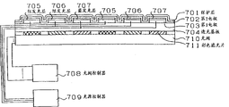
在本实施例中,示出在实施例1的结构中在从发光层看,在光射出一侧还配置了彩色滤光片之例。图7中示出本实施例的显示装置的剖面结构。In this embodiment, an example is shown in which a color filter is arranged on the light emitting side as viewed from the light-emitting layer in the structure of the first embodiment. FIG. 7 shows a cross-sectional structure of the display device of this embodiment.
首先,使与透明基板704的与光源部件相反的一侧上应该形成各发光层的位置对应来形成红色(R)、绿色(G)及蓝色(B)的彩色滤光片711,与各自的图形对应来形成成为第1电极的透明导电膜,进行构图。利用与实施例1同样的方法及结构,在该基板上得到该图中所示的剖面结构的显示装置。First, red (R), green (G) and blue (B) color filters 711 are formed corresponding to the positions where the light-emitting layers are to be formed on the side of the transparent substrate 704 opposite to the light source component, and the respective color filters 711 are formed. A transparent conductive film to be the first electrode is formed corresponding to the pattern and patterned. Using the same method and structure as in Example 1, a display device having the cross-sectional structure shown in the figure was obtained on the substrate.
利用本实施例,在作为发光层的色纯度不充分的情况下,可利用彩色滤光片进行色补正,可实现与NTSC色度同等的色度。According to this embodiment, when the color purity of the light-emitting layer is insufficient, color correction can be performed using a color filter, and chromaticity equivalent to NTSC chromaticity can be realized.
在本实施例中,使用了RGB彩色滤色片,但是,也可以对照发光层的发光色来调整彩色滤光片的颜色。In this embodiment, RGB color filters are used, however, the color of the color filters may be adjusted in accordance with the light emission color of the light emitting layer.
(实施例5)(Example 5)
在本实施例中,示出在实施例1的结构中在从发光层看,在光射出一侧配置了光扩散层之例。图8中示出本实施例的显示装置的剖面结构。在实施例1中作成的光源的光射出一侧(在透光基板804与光阀810之间)配置了光扩散板811。In this example, in the structure of Example 1, the example in which the light-diffusion layer was arrange|positioned on the light emitting side as seen from a light emitting layer is shown. FIG. 8 shows a cross-sectional structure of the display device of this embodiment. A light diffusion plate 811 is disposed on the light emitting side of the light source prepared in Example 1 (between the light-transmitting substrate 804 and the light valve 810 ).
由此,即使直视显示装置,RGB发光源的边界也被适当地冲淡,可看到把整个光源面点亮成RGB那样。As a result, even if the display device is viewed directly, the boundaries of the RGB light sources are properly diluted, and it can be seen that the entire light source surface is lit in RGB.
(实施例6)(Example 6)
在本实施例中,示出以与实施例5的显示装置同样的考虑方法的光源的基板本身,使用了具有光扩散性的基板之例。图9中示出本实施例的显示装置的剖面结构。In the present example, an example in which a light-diffusing substrate is used for the substrate itself of the light source in the same consideration as that of the display device of the fifth example is shown. FIG. 9 shows a cross-sectional structure of the display device of this embodiment.
除了使用了光扩散板904作为实施例1的透光基板之外,与实施例1同样地作成光源。由此,可非常简便地放弃色发光源。此外,由于并不增加部件,故仍保持为薄型轻量,可提高显示品质。A light source was produced in the same manner as in Example 1 except that the light diffusion plate 904 was used as the light-transmitting substrate of Example 1. FIG. As a result, a colored light source can be dispensed with very simply. In addition, since there are no additional components, it remains thin and lightweight, which improves display quality.
(实施例7)(Example 7)
在本实施例中,示出在对上述实施例的显示装置的光源中的发光材料进行构图以形成发光层时,把上述发光材料液化,使用印刷法或喷墨法来形成该发光层之例。图10中示出使用喷墨法的本实施例的显示装置的光源的发光层的形成的概念。In this example, when patterning the light-emitting material in the light source of the display device of the above-mentioned example to form a light-emitting layer, the above-mentioned light-emitting material is liquefied, and an example of forming the light-emitting layer by using a printing method or an inkjet method is shown. . FIG. 10 shows the concept of forming the light emitting layer of the light source of the display device of this embodiment using the inkjet method.
首先,在透光基板1003上形成透明电极,进行构图,设置第1电极1002的图形,还在电极间设置隔壁1001。其次,使用喷墨法如图中所示,在隔壁1001之间的电极1002上顺序形成发光层(红发光层1004、绿发光层1005及蓝发光层1006)。再形成第2电极以后的部件。First, transparent electrodes are formed on the light-transmitting substrate 1003, patterned, the pattern of the first electrode 1002 is provided, and partition walls 1001 are provided between the electrodes. Next, as shown in the figure, light-emitting layers (red light-emitting
利用该结构,可不使用真空工艺,非常简便地作成光源部。With this structure, the light source unit can be fabricated very simply without using a vacuum process.
以迄今所使用的印刷法来代替喷墨法,也同样可以实施。此外,在本实施例中作为发光材料使用了能液化的有机材料,但是,即使是无机EL材料如果使用能液化的材料,也同样可以作成。例如,如果使用烷氧基化金属,则由于容易溶于酒精中,故可以使用。涂布后,进行烧焙,把烷氧基去除即可。It is also possible to replace the ink-jet method with the conventional printing method. In addition, in this embodiment, a liquefiable organic material is used as the luminescent material, but even an inorganic EL material can be formed similarly if a liquefiable material is used. For example, if a metal alkoxide is used, it can be used because it is easily soluble in alcohol. After coating, it can be calcined to remove the alkoxy group.
此外,如实施例2中的面状光源的结构那样,在对第2电极也进行构图的情况下,可利用本实施例的隔壁1001,与阴极蒸镀同时来进行构图。In addition, when patterning is also performed on the second electrode as in the structure of the planar light source in Example 2, patterning can be performed simultaneously with cathode vapor deposition using the barrier ribs 1001 of this example.
(实施例8)(Embodiment 8)
在本实施例中,特征在于,把上述各色发光材料在同一电压下的发光亮度与各色发光层的发光面积之积设定为白平衡所能取的值。图11中示出本实施例的显示装置的剖面结构。In this embodiment, it is characterized in that the product of the luminance of each color luminescent material under the same voltage and the luminous area of each color luminescent layer is set as a value that can be taken by the white balance. FIG. 11 shows a cross-sectional structure of the display device of this embodiment.
作为在本实施例中使用的发光材料使用了在电压5伏时发光亮度比为红∶绿∶蓝=1∶10∶2的材料。一般来说,如果白平衡为3∶12∶10,别人眼观看时可看成白色,这一点是周知的。因此,如果假定红、绿、蓝的发光面积分别为X、Y、Z,作为1xx=3,10xy=12,2xz=10,得到X∶Y∶Z=3∶1.2∶5。该比例为各色的发光面积比。图11中示出使红发光层(1105)、绿发光层(1106)、蓝发光层(1107)的平面面积不同,这样来调整发光面积的情况。再者,该图中所示的显示装置的其它结构部分实质上与实施例1的结构相同。As the luminescent material used in this embodiment, a material having a luminance ratio of red:green:blue=1:10:2 at a voltage of 5 volts was used. Generally speaking, if the white balance is 3:12:10, it can be seen as white by other people's eyes, which is well known. Therefore, if it is assumed that the light emitting areas of red, green, and blue are X, Y, and Z, respectively, as 1xx=3, 10xy=12, and 2xz=10, X:Y:Z=3:1.2:5 is obtained. This ratio is the light emitting area ratio of each color. FIG. 11 shows the case where the red light emitting layer (1105), the green light emitting layer (1106), and the blue light emitting layer (1107) have different planar areas to adjust the light emitting area. In addition, other structural parts of the display device shown in this figure are substantially the same as those of the first embodiment.
利用该结构,在把亮度特性不同的发光材料组合使用的情况下,可在取得白平衡的同时把光源部的驱动电压定为一个电压,可简化电路。With this configuration, when light emitting materials having different luminance characteristics are used in combination, the driving voltage of the light source unit can be set to one voltage while achieving white balance, thereby simplifying the circuit.
(实施例9)(Example 9)
在本实施例中,示出上述发光材料由有机化合物或有机高分子构成之例。In this embodiment, an example in which the above-mentioned light-emitting material is composed of an organic compound or an organic polymer is shown.
作为实施例1的发光层形成了下面所示的空穴注入层及发光层,再有,作为第2电极形成了下面所示的阴极。驱动电压为直流5伏,由于作为光源控制器成为直流切换电路,故是非常简便的电路。亮度为100cd/m2,功耗为0.5w。A hole injection layer and a light emitting layer shown below were formed as a light emitting layer in Example 1, and a cathode shown below was formed as a second electrode. The driving voltage is DC 5V, and since it becomes a DC switching circuit as a light source controller, it is a very simple circuit. The brightness is 100cd/m 2 , and the power consumption is 0.5w.
空穴注入层为三苯胺衍生物,但是,只要是具有同样效果的材料就可以使用。例如TPD、TAD、m-MTDATA等。The hole injection layer is a triphenylamine derivative, but any material can be used as long as it has the same effect. For example, TPD, TAD, m-MTDATA, etc.
此外,在酞菁染料、聚噻吩烷、聚苯胺或聚乙烯咔唑等的衍生物中,只要是具有导电性且容易制膜的材料就同样可以使用。In addition, among derivatives such as phthalocyanine dye, polythiophene, polyaniline, polyvinylcarbazole, and the like, any material that has conductivity and is easy to form a film can be similarly used.
在发光层中,作为红发光材料使用掺杂了DCM的Alq3,作为绿发光材料使用掺杂了红荧烯的Alq3,作为蓝色发光材料使用了DPVBi,但是,只要是能使用蒸镀法制膜的发光材料就同样可以使用。此外,在蒸镀法之外,只要是能形成发光层的方法其它发光材料也同样可以使用。In the light-emitting layer, Alq3 doped with DCM is used as the red light-emitting material, Alq3 doped with rubrene is used as the green light-emitting material, and DPVBi is used as the blue light-emitting material. The luminescent material of the same can be used. In addition, other luminescent materials can be similarly used as long as they can form a luminescent layer other than the vapor deposition method.
作为阴极可使用蒸镀了镁和银的合金的材料,但是,也可以利用溅射法或电镀等湿式法来形成,此外,钙、锂、铝等如果是包含功函数比作为第1电极的阳极小的材料,则同样可以使用。As the cathode, an alloy of magnesium and silver can be deposited. However, it can also be formed by a wet method such as sputtering or electroplating. In addition, if calcium, lithium, aluminum, etc. contain work function ratios as the first electrode Materials with small anodes can also be used.
(实施例10)(Example 10)
在本实施例中,示出在以构图方式形成实施例9中多种发光材料内的至少1种发光材料之后,在整个面上对具有发波长比其短的发光材料进行制膜,来形成发光层之例。图12中示出本实施例的显示装置的剖面结构。In this example, it is shown that after patterning at least one of the various luminescent materials in Example 9, a luminescent material having a shorter emission wavelength is formed on the entire surface to form a An example of a luminescent layer. FIG. 12 shows the cross-sectional structure of the display device of this embodiment.
在透光基板1204上形成由进行了构图的ITO等透明导电膜构成的第1电极1203,利用喷墨法顺序在其上进行构图形成红和绿的发光材料,得到红发光层1205和绿发光层1206。其次,在整个面上涂布蓝发光材料形成蓝发光层1207,在形成第2电极1202之后进行密封,形成保护层1201。上面的方法与实施例1同样地进行。A first electrode 1203 made of a patterned transparent conductive film such as ITO is formed on a light-transmitting substrate 1204, and red and green light-emitting materials are sequentially patterned on it by an inkjet method to obtain a red light-emitting
按照该方法,不需要蓝发光材料的构图7。来自蓝发光层1207的蓝色发光在红和绿发光区中激励红或绿发光层(1205,1206),分别变换成红或绿的发光。或者,通过蓝发光层的电子在红或绿发光层内与空穴复合,激励红或绿发光层,使之发红光或绿光。According to this method, patterning 7 of the blue luminescent material is not required. The blue light emission from the blue light emitting layer 1207 excites the red or green light emitting layers (1205, 1206) in the red and green light emitting regions, and is converted into red or green light emission, respectively. Alternatively, electrons passing through the blue light-emitting layer recombine with holes in the red or green light-emitting layer to excite the red or green light-emitting layer to emit red or green light.
在本实施例中,可使用一般的印刷法或蒸镀法来代替喷墨法。此外,可在形成蓝色发光层时,使用蒸镀法、旋转涂布法、印刷法等。In this embodiment, a general printing method or an evaporation method may be used instead of the inkjet method. In addition, when forming the blue light-emitting layer, a vapor deposition method, a spin coating method, a printing method, or the like can be used.
(实施例11)(Example 11)
在本实施例中,示出以条状形成多层有机发光层,并且,上述各色条的1组的间距P、与上述平面型光阀的光阀面与上述发光层的距离d具有p/d<1.1的关系之例。图13中示出本实施例的显示装置的剖面结构。In the present embodiment, it is shown that a multilayer organic light-emitting layer is formed in a stripe shape, and the pitch P of one group of the above-mentioned color stripes and the distance d between the light valve surface of the above-mentioned planar light valve and the above-mentioned light-emitting layer have p/ An example of the relationship of d<1.1. FIG. 13 shows the cross-sectional structure of the display device of this embodiment.
按照人眼,由于RGB中色的亮度离散在5%以内则不能识别RGB各色,故满足该条件的p与d之关系为上述中所示的关系。在实际结构中,在厚度为1mm的透光基板1304上以间距为400μm的条状形成ITO并进行构图以得到第1电极1303,在溶液状下用喷墨法在其上构图涂布了RGB的各发光材料作成各自宽度为400μm的条(红发光层1305、绿发光层1306、蓝发光层1307)。干燥后,形成作为对置电极的第2电极1302,形成保护层1301进行了密封。在这样作成的光源中,把液晶光阀1310与其光阀面1311配置起来使得各发光层的距离d、与各色条的1组的间距P成为p/d<1.1的关系,在利用与实施例1同样的驱动电路进行了驱动后,即使不使用扩散板也能进行足够均匀的彩色显示。当然,利用与扩散层组合起来可得到进一步均匀的显示。此外,在本实施例中,以条状的图形示出了实施例,但是,在不脱离本实施例宗旨的范围内,可对图形进行变更。According to the human eye, since the luminance of the RGB intermediate colors is scattered within 5%, the RGB colors cannot be recognized, so the relationship between p and d satisfying this condition is the relationship shown above. In the actual structure, ITO is formed in strips with a pitch of 400 μm on a light-transmitting substrate 1304 with a thickness of 1 mm and patterned to obtain the first electrode 1303, and RGB is patterned and coated on it by inkjet method in a solution state. Each of the luminescent materials is made into stripes (red luminescent layer 1305, green luminescent layer 1306, blue luminescent layer 1307) each with a width of 400 μm. After drying, a second electrode 1302 as a counter electrode was formed, and a protective layer 1301 was formed and sealed. In the light source made in this way, the liquid crystal light valve 1310 and its light valve surface 1311 are arranged so that the distance d of each light emitting layer and the pitch P of one group of each color stripe become the relationship of p/d<1.1. 1 When driven by the same drive circuit, a sufficiently uniform color display can be performed without using a diffuser plate. Of course, a further uniform display can be obtained by combining with a diffusion layer. In addition, in this embodiment, the embodiment is shown as a bar graph, but the graph can be changed within the scope not departing from the gist of this embodiment.
(实施例12)(Example 12)
在本实施例中,示出上述平面型光调制面板为液晶光阀,把1/4波长片插入到上述光源与上述液晶光阀之间,把该1/4波长片的延伸轴配置成相对于与其相接的液晶光阀的偏振片之偏振方向倾斜约45°之例。图14中示出本实施例的显示装置的剖面图。In this embodiment, the above-mentioned planar light modulation panel is shown as a liquid crystal light valve, a 1/4 wavelength plate is inserted between the above-mentioned light source and the above-mentioned liquid crystal light valve, and the extension axes of the 1/4 wavelength plate are arranged to be opposite to each other. An example in which the polarization direction of the polarizer of the liquid crystal light valve connected to it is inclined by about 45°. FIG. 14 shows a cross-sectional view of the display device of this embodiment.
用本实施例作成的显示装置中,面状光源部分的基本结构与实施例11中的光源的结构相同。在本实施例中,把1/4波长片配置到实施11的结构中光源的透光基板(1404)与液晶光阀(1411)之间,使之相对于与其相接的液晶光阀的偏振片之偏振方向倾斜约45°。由此,外部光的反射大体上没有了,对比度成为50∶1以上。通过插入1/4波长片,大大提高了目视性。In the display device fabricated in this embodiment, the basic structure of the planar light source portion is the same as that of the light source in the eleventh embodiment. In this embodiment, the 1/4 wavelength plate is arranged between the light-transmitting substrate (1404) of the light source and the liquid crystal light valve (1411) in the structure of Embodiment 11, so that it is relative to the polarization of the liquid crystal light valve connected to it. The polarization direction of the sheet is tilted by about 45°. As a result, the reflection of external light is almost eliminated, and the contrast ratio becomes 50:1 or more. Visibility has been greatly improved by inserting a 1/4 wavelength plate.
如果对本实施例显示装置的表面进行减反射处理或防眩处理,则可进一步提高目视性。If anti-reflection treatment or anti-glare treatment is performed on the surface of the display device of this embodiment, the visibility can be further improved.
(实施例13)(Example 13)
在本实施例中,示出上述光源内的发光层由有机化合物或有机高分子作成,而且使之取向于1个轴的方向上,使来自上述发光层的发光的偏振方向与液晶光阀在光源一侧的偏振片的偏振方向一致之例。在基本上与实施例11相同的结构中,使发光层的有机物质取向,进行配置以使来自发光层的发光的主偏振方向与液晶光阀的偏振片之透射轴一致。由此,使投入的电能无浪费地变换成偏振光,成为能够对光阀进行投入,成为与迄今相比能够得到接近于2倍效率的情况。In this embodiment, it is shown that the light-emitting layer in the above-mentioned light source is made of organic compound or organic polymer, and it is oriented in the direction of one axis, and the polarization direction of the light from the above-mentioned light-emitting layer is aligned with the liquid crystal light valve. An example where the polarization directions of the polarizers on the light source side are the same. In basically the same structure as in Example 11, the organic material of the light-emitting layer was oriented and arranged so that the main polarization direction of light emitted from the light-emitting layer coincided with the transmission axis of the polarizer of the liquid crystal light valve. Thereby, the input electric energy can be converted into polarized light without waste, and it becomes possible to input into the light valve, and it becomes possible to obtain nearly double the efficiency compared with the conventional one.
(实施例14)(Example 14)
在本实施例中,示出在与平面状光调制面板组合的,具有多个发光区的面状光源中的发光区的图形形状之变形例。图15中,示出本实施例的面状光源的发光区的图形形状。In this embodiment, a modified example of the pattern shape of the light emitting regions in a planar light source having a plurality of light emitting regions combined with a planar light modulation panel is shown. In FIG. 15, the figure shape of the light emitting area of the planar light source of this embodiment is shown.
在该图中所示的面状光源中,在基板10上以螺旋状形成了红色发光的发光区400R、绿色发光的发光区400G、蓝色发光的发光区400B。在此,区域400R、400G、400B的每一个为在第1与第2这一对电极之间夹持有机或无机的各色发光的发光材料(发光层)的场致发光元件(EL元件)的结构,较为理想的是,各场致发光元件的结构本身为在平面上如图所示那样的螺旋形的图形形状。In the planar light source shown in the figure, a red
按照这样的结构,构成发光元件的电极的膜(阴极膜、阳极膜)不存在基板上交叉的区域,不需要形成设置在这样的交叉区域中的绝缘膜的图形(例如,在图1中所示的例子中的绝缘膜105变成不需要了),面状光源的制造工艺本身变得更加容易。According to such a structure, the film (cathode film, anode film) that constitutes the electrode of the light-emitting element does not have the area that intersects on the substrate, and it is not necessary to form the pattern of the insulating film that is arranged in such an intersecting area (for example, shown in FIG. The insulating film 105 in the illustrated example becomes unnecessary), and the manufacturing process itself of the planar light source becomes easier.
(实施例15)(Example 15)
在本实施例中,示出在与平面状光调制面板组合使用的面状光源中的发光区的图形形状之又一个变形例。图16中,示出本实施例的面状光源的发光区的图形形状。In this embodiment, another modified example of the pattern shape of the light emitting area in the planar light source used in combination with the planar light modulation panel is shown. In FIG. 16, the figure shape of the light emitting area of the planar light source of this embodiment is shown.
在该图中所示的面状光源中构成了下述的光源,把在基板10上以螺旋状形成了红色发光的发光区500R、绿色发光的发光区500G、蓝色发光的发光区500B的图形作为1个单元,用4个这样的单元遍布所需要的面积进行发光。在此,与实施例14相同,各单元的区域500R、500G,500B的每一个为在第1与第2这一对电极之间夹持有机或无机的各色发光的发光材料(发光层)的EL元件的结构,较为理想的是,各EL元件的结构本身为在平面上如图所示那样的螺旋形的图形形状。In the planar light source shown in this figure, the following light source is constituted. The red light-emitting
再有,对每个单元从4个部位、在图16之例中为从基板10的4个角附近的部分供给使EL元件发光的电流。与用连续的螺旋状元件来构成相比,通过进行分割来配置螺旋状元件可缩短EL元件的线状图形的长度,即能够抑制因构成EL元件的电极及布线的电阻所引起的电压降及发热。In addition, a current for causing the EL element to emit light is supplied to each cell from four places, in the example of FIG. 16 , from parts near the four corners of the
如上所述,按照本发明,在使用了时分割彩色光源的显示装置中,由平面型调制面板与设置在其背面上的面状光源的结构构成,作为面状光源使用了由有机或无机的EL元件构成的发光区,由此,可降低功耗,能够大大紧凑化。此外,同时可使色纯度提高,还能显著地提高对比度。As described above, according to the present invention, in the display device using the time-divided color light source, it is composed of a planar modulation panel and a planar light source arranged on the back thereof. As the planar light source, organic or inorganic The light-emitting area composed of EL elements can reduce power consumption and greatly reduce the size of the light-emitting area. In addition, at the same time, the color purity can be improved, and the contrast ratio can be significantly improved.
除此之外,在本发明中,通过使用在平面上的螺旋线形状作为面状光源中的发光区的图形形状,特别是在利用EL元件来形成发光区的情况下,可以实现结构简单,抑制了布线电阻及不需要的发热的光源。In addition, in the present invention, by using a spiral shape on a plane as the figure shape of the light emitting region in the planar light source, especially in the case of using an EL element to form the light emitting region, a simple structure can be achieved, A light source that suppresses wiring resistance and unnecessary heat generation.
工业上利用的可能性Possibility of industrial use
本发明的显示装置可优选地用于具备下述装置的,像液晶投影仪那样的投射型显示装置等的电子装置中:要求高清晰度图像显示的膝上型个人计算机(PC)、电视机、录像器型或监视器直观型磁带录像机、车辆导航装置、电子记事本、台式电子计算器、文字处理器、工作站(EWS)、携带电话机、可视电话机、POS终端、寻呼机及触摸屏等。The display device of the present invention can be preferably used in an electronic device such as a projection display device such as a liquid crystal projector equipped with: a laptop personal computer (PC), a television set that requires high-definition image display , video recorder type or monitor intuitive tape video recorder, vehicle navigation device, electronic notebook, desktop electronic calculator, word processor, workstation (EWS), portable telephone, videophone, POS terminal, pager and touch screen, etc. .
Claims (25)
Applications Claiming Priority (3)
| Application Number | Priority Date | Filing Date | Title |
|---|---|---|---|
| JP210011/1998 | 1998-07-24 | ||
| JP21001198 | 1998-07-24 | ||
| JP210011/98 | 1998-07-24 |
Related Child Applications (1)
| Application Number | Title | Priority Date | Filing Date |
|---|---|---|---|
| CNB2005101247036A Division CN100432788C (en) | 1998-07-24 | 1999-07-23 | Display device |
Publications (2)
| Publication Number | Publication Date |
|---|---|
| CN1286783A CN1286783A (en) | 2001-03-07 |
| CN1237496C true CN1237496C (en) | 2006-01-18 |
Family
ID=16582360
Family Applications (2)
| Application Number | Title | Priority Date | Filing Date |
|---|---|---|---|
| CNB998016756A Expired - Lifetime CN1237496C (en) | 1998-07-24 | 1999-07-23 | display device |
| CNB2005101247036A Expired - Lifetime CN100432788C (en) | 1998-07-24 | 1999-07-23 | Display device |
Family Applications After (1)
| Application Number | Title | Priority Date | Filing Date |
|---|---|---|---|
| CNB2005101247036A Expired - Lifetime CN100432788C (en) | 1998-07-24 | 1999-07-23 | Display device |
Country Status (7)
| Country | Link |
|---|---|
| US (1) | US6437769B1 (en) |
| EP (1) | EP1018718B1 (en) |
| KR (1) | KR100496071B1 (en) |
| CN (2) | CN1237496C (en) |
| DE (1) | DE69927235T2 (en) |
| TW (1) | TW507103B (en) |
| WO (1) | WO2000005703A1 (en) |
Families Citing this family (60)
| Publication number | Priority date | Publication date | Assignee | Title |
|---|---|---|---|---|
| US6366025B1 (en) * | 1999-02-26 | 2002-04-02 | Sanyo Electric Co., Ltd. | Electroluminescence display apparatus |
| DE19916745A1 (en) * | 1999-04-13 | 2000-10-19 | Mannesmann Vdo Ag | Light-emitting diode with organic light-emitting substances for generating light with mixed colors |
| US6590553B1 (en) * | 1999-07-23 | 2003-07-08 | Nec Corporation | Liquid crystal display device and method for driving the same |
| TW494447B (en) | 2000-02-01 | 2002-07-11 | Semiconductor Energy Lab | Semiconductor device and manufacturing method thereof |
| JP4491632B2 (en) * | 2000-04-07 | 2010-06-30 | 日本電気株式会社 | Driving method of liquid crystal display device |
| US7579203B2 (en) * | 2000-04-25 | 2009-08-25 | Semiconductor Energy Laboratory Co., Ltd. | Light emitting device |
| US6838819B2 (en) * | 2000-06-19 | 2005-01-04 | Lg Electronics Inc. | Full color organic EL display panel, manufacturing method thereof and driving circuit thereof |
| AU2001295943A1 (en) * | 2000-10-17 | 2002-04-29 | Matsushita Electric Industrial Co., Ltd. | Liquid crystal display and its producing method |
| US6872586B2 (en) * | 2000-10-17 | 2005-03-29 | Seiko Epson Corporation | Method of manufacture of active matrix substrate and liquid crystal display device |
| EP2309315B1 (en) | 2001-02-27 | 2020-07-29 | Dolby Laboratories Licensing Corporation | A method and device for displaying an image |
| TW559746B (en) * | 2001-05-15 | 2003-11-01 | Koninkl Philips Electronics Nv | Method of driving an organic electroluminescent display device and display device suitable for said method |
| US6809481B2 (en) * | 2002-02-28 | 2004-10-26 | Semiconductor Energy Laboratory Co., Ltd. | Light emitting device and electric device using the same |
| US8687271B2 (en) | 2002-03-13 | 2014-04-01 | Dolby Laboratories Licensing Corporation | N-modulation displays and related methods |
| AU2003212146A1 (en) | 2002-03-13 | 2003-09-22 | The University Of British Columbia | High dynamic range display devices |
| EP1507444A4 (en) * | 2002-05-17 | 2008-01-23 | Print Labo Co Ltd | EL ELECTROLUMINESCENT DEVICE |
| EP1529647A4 (en) * | 2002-08-14 | 2007-07-25 | Citizen Holdings Co Ltd | Liquid crystal exposure device |
| JP2006520478A (en) * | 2003-01-17 | 2006-09-07 | ダイオード・ソリューションズ・インコーポレーテッド | Display using organic materials |
| DE10317258B4 (en) * | 2003-04-14 | 2006-09-07 | Eads Deutschland Gmbh | Adjustment mechanism for a shape-variable wing |
| GB2403023A (en) * | 2003-06-20 | 2004-12-22 | Sharp Kk | Organic light emitting device |
| TWI278827B (en) * | 2004-05-12 | 2007-04-11 | Seiko Epson Corp | Display equipment and electronic apparatus |
| KR100619627B1 (en) * | 2004-05-27 | 2006-09-08 | 엘지.필립스 엘시디 주식회사 | Luminance Control Device and Method of Liquid Crystal Display |
| US7540978B2 (en) | 2004-08-05 | 2009-06-02 | Novaled Ag | Use of an organic matrix material for producing an organic semiconductor material, organic semiconductor material and electronic component |
| JP2008509565A (en) | 2004-08-13 | 2008-03-27 | ノヴァレッド・アクチエンゲゼルシャフト | Laminate for luminescent component |
| KR100724157B1 (en) * | 2004-09-09 | 2007-06-04 | (주)케이디티 | Fabrication method of organic electroluminescent device by insulating film patterning |
| EP1648042B1 (en) | 2004-10-07 | 2007-05-02 | Novaled AG | A method for doping a semiconductor material with cesium |
| DE502005002342D1 (en) * | 2005-03-15 | 2008-02-07 | Novaled Ag | Light-emitting component |
| JP4684046B2 (en) * | 2005-03-30 | 2011-05-18 | 三洋電機株式会社 | Display device |
| ATE381117T1 (en) | 2005-04-13 | 2007-12-15 | Novaled Ag | ARRANGEMENT FOR A PIN-TYPE ORGANIC LIGHT-EMITTING DIODE AND METHOD FOR PRODUCING IT |
| EP1727221B1 (en) | 2005-05-27 | 2010-04-14 | Novaled AG | Transparent organic light emitting diode |
| EP1729346A1 (en) * | 2005-06-01 | 2006-12-06 | Novaled AG | Light-emitting device with an electrode arrangement |
| EP1739765A1 (en) * | 2005-07-01 | 2007-01-03 | Novaled AG | Organic light-emitting diode and stack of organic light emitting diodes |
| KR100685845B1 (en) * | 2005-10-21 | 2007-02-22 | 삼성에스디아이 주식회사 | Organic light emitting display device and manufacturing method thereof |
| EP1806795B1 (en) * | 2005-12-21 | 2008-07-09 | Novaled AG | Organic Device |
| DE602006001930D1 (en) * | 2005-12-23 | 2008-09-04 | Novaled Ag | of organic layers |
| US8003999B2 (en) * | 2005-12-30 | 2011-08-23 | Samsung Mobile Display Co., Ltd. | Organic light emitting device |
| EP1808909A1 (en) | 2006-01-11 | 2007-07-18 | Novaled AG | Electroluminescent light-emitting device |
| US7999372B2 (en) * | 2006-01-25 | 2011-08-16 | Samsung Mobile Display Co., Ltd. | Organic light emitting display device and method of fabricating the same |
| BRPI0710313A2 (en) * | 2006-04-04 | 2011-08-09 | 6N Silicon Inc | method for silicon purification |
| EP1848049B1 (en) * | 2006-04-19 | 2009-12-09 | Novaled AG | Light emitting device |
| DE102006052029B4 (en) * | 2006-09-22 | 2020-01-09 | Osram Oled Gmbh | Light emitting device |
| US8884322B2 (en) | 2006-09-22 | 2014-11-11 | Osram Opto Semiconductor Gmbh | Light-emitting device |
| TW200818979A (en) * | 2006-09-29 | 2008-04-16 | Osram Opto Semiconductors Gmbh | Organic light-emitting component, device with the same, lighting equipment and display device |
| US8222077B2 (en) * | 2006-11-07 | 2012-07-17 | Cbrite Inc. | Metal-insulator-metal (MIM) devices and their methods of fabrication |
| US7898042B2 (en) | 2006-11-07 | 2011-03-01 | Cbrite Inc. | Two-terminal switching devices and their methods of fabrication |
| US9741901B2 (en) | 2006-11-07 | 2017-08-22 | Cbrite Inc. | Two-terminal electronic devices and their methods of fabrication |
| DE102006059509B4 (en) * | 2006-12-14 | 2012-05-03 | Novaled Ag | Organic light-emitting element |
| MX2009008192A (en) * | 2007-02-01 | 2009-08-12 | Dolby Lab Licensing Corp | Calibration of displays having spatially-variable backlight. |
| DE102007019260B4 (en) * | 2007-04-17 | 2020-01-16 | Novaled Gmbh | Non-volatile organic storage element |
| US20090322800A1 (en) | 2008-06-25 | 2009-12-31 | Dolby Laboratories Licensing Corporation | Method and apparatus in various embodiments for hdr implementation in display devices |
| DE102008030821A1 (en) * | 2008-06-30 | 2009-12-31 | Osram Opto Semiconductors Gmbh | An electroluminescent device and method of making an electroluminescent device |
| DE102008036062B4 (en) | 2008-08-04 | 2015-11-12 | Novaled Ag | Organic field effect transistor |
| DE102008036063B4 (en) * | 2008-08-04 | 2017-08-31 | Novaled Gmbh | Organic field effect transistor |
| US20100214282A1 (en) | 2009-02-24 | 2010-08-26 | Dolby Laboratories Licensing Corporation | Apparatus for providing light source modulation in dual modulator displays |
| CN201844304U (en) * | 2010-09-26 | 2011-05-25 | 北京京东方光电科技有限公司 | Regionally controllable backlight source |
| FR2971345A1 (en) * | 2011-02-07 | 2012-08-10 | Commissariat Energie Atomique | LCD for microdisplay in e.g. headphone, has backlight sources, each including emissive zones, where emissive zones are formed by organic layer of organic LED that emits light in color corresponding to emissive zones |
| KR101832957B1 (en) | 2011-05-31 | 2018-02-28 | 엘지전자 주식회사 | Micro shutter display device |
| JP6133301B2 (en) | 2012-09-10 | 2017-05-24 | パイオニア株式会社 | Light emitting device |
| KR102084718B1 (en) * | 2013-08-19 | 2020-03-05 | 삼성디스플레이 주식회사 | Backlight unit and display device including the same |
| CN105242447A (en) * | 2015-11-09 | 2016-01-13 | 武汉华星光电技术有限公司 | Transparent displayer |
| CN113423154B (en) * | 2021-06-01 | 2023-03-10 | 北京大学深圳研究生院 | Electroluminescence tetrode integrating light emission, switch and color control and its control method |
Family Cites Families (31)
| Publication number | Priority date | Publication date | Assignee | Title |
|---|---|---|---|---|
| FI73325C (en) * | 1985-03-05 | 1987-09-10 | Elkoteade Ag | FOERFARANDE FOER ALSTRING AV INDIVIDUELLT REGLERBARA BILDELEMENT OCH PAO DESSA BASERAD FAERGDISPLAY. |
| JPH01179914A (en) * | 1988-01-12 | 1989-07-18 | Nec Corp | Liquid crystal color display device |
| JPH02165592A (en) | 1988-12-19 | 1990-06-26 | Sharp Corp | Thin el element |
| JPH03187192A (en) | 1989-12-18 | 1991-08-15 | Seiko Epson Corp | Light emitting element |
| DE69025341T2 (en) * | 1989-12-22 | 1996-08-29 | Sarnoff David Res Center | Raster sequential display system incorporating a rear-illuminable array of liquid crystal picture elements and imaging method |
| JPH03269995A (en) | 1990-03-16 | 1991-12-02 | Ricoh Co Ltd | Method for manufacturing electroluminescent device |
| US5248917A (en) * | 1990-07-31 | 1993-09-28 | Sanyo Electric Co., Ltd. | Flat fluorescent lamp and liquid crystal projector incorporating same |
| JPH0519257A (en) | 1991-07-15 | 1993-01-29 | Japan Aviation Electron Ind Ltd | Color liquid crystal display |
| JPH05264988A (en) | 1992-03-18 | 1993-10-15 | Nec Ic Microcomput Syst Ltd | Color liquid crystal display |
| JPH05346570A (en) | 1992-06-15 | 1993-12-27 | Seiko Instr Inc | Liquid crystal display device |
| JPH067149A (en) | 1992-06-25 | 1994-01-18 | Mitsubishi Heavy Ind Ltd | Measuring device of microbial cell concentration |
| US5808410A (en) * | 1992-07-28 | 1998-09-15 | Philips Electronics North America Corporation | Flat panel light source for liquid crystal displays |
| JP3121932B2 (en) * | 1992-09-28 | 2001-01-09 | 三菱電機株式会社 | Liquid crystal display |
| JPH06301004A (en) | 1993-04-13 | 1994-10-28 | Rohm Co Ltd | Light emitting device and liquid crystal display device formed by using the light emitting device |
| JPH06301032A (en) | 1993-04-13 | 1994-10-28 | Rohm Co Ltd | Light emitting device and liquid crystal display device formed by using this light source device |
| JP2747413B2 (en) | 1993-09-17 | 1998-05-06 | 筒中プラスチック工業株式会社 | Thin surface emitting device |
| JPH083688A (en) | 1994-06-22 | 1996-01-09 | Kawasaki Steel Corp | Hot-rolled steel sheet for high toughness square steel pipe and high toughness square steel pipe excellent in Zn plating cracking resistance |
| JP2931211B2 (en) * | 1994-09-13 | 1999-08-09 | 出光興産株式会社 | Organic EL device |
| JPH08153582A (en) | 1994-11-25 | 1996-06-11 | Nippon Seiki Co Ltd | Distributed electroluminescent device |
| WO1996033483A1 (en) * | 1995-04-18 | 1996-10-24 | Cambridge Display Technology Limited | A display |
| DE69613093T2 (en) | 1995-08-21 | 2001-11-22 | Koninklijke Philips Electronics N.V., Eindhoven | ELECTROLUMINESCENT DEVICE |
| JP3627831B2 (en) | 1995-10-04 | 2005-03-09 | 沖田 雅也 | Liquid crystal display |
| JPH09114421A (en) | 1995-10-19 | 1997-05-02 | Asahi Glass Co Ltd | Color liquid crystal display |
| JPH09127885A (en) | 1995-10-30 | 1997-05-16 | Sony Corp | Display element |
| JP3756230B2 (en) | 1995-11-14 | 2006-03-15 | 株式会社半導体エネルギー研究所 | Display device |
| JP3418508B2 (en) * | 1995-11-28 | 2003-06-23 | シャープ株式会社 | Projection type image display device |
| JPH1012379A (en) * | 1996-06-24 | 1998-01-16 | Idemitsu Kosan Co Ltd | Multicolor light emitting device and method of manufacturing the same |
| JPH1039791A (en) * | 1996-07-22 | 1998-02-13 | Mitsubishi Electric Corp | Organic electroluminescence display device |
| JP3899566B2 (en) * | 1996-11-25 | 2007-03-28 | セイコーエプソン株式会社 | Manufacturing method of organic EL display device |
| JP3540534B2 (en) * | 1996-12-20 | 2004-07-07 | 三洋電機株式会社 | Color video display |
| JPH10189244A (en) | 1996-12-24 | 1998-07-21 | Casio Comput Co Ltd | Electroluminescence panel |
-
1999
- 1999-07-23 CN CNB998016756A patent/CN1237496C/en not_active Expired - Lifetime
- 1999-07-23 EP EP99931529A patent/EP1018718B1/en not_active Expired - Lifetime
- 1999-07-23 TW TW088112571A patent/TW507103B/en not_active IP Right Cessation
- 1999-07-23 WO PCT/JP1999/003980 patent/WO2000005703A1/en not_active Ceased
- 1999-07-23 CN CNB2005101247036A patent/CN100432788C/en not_active Expired - Lifetime
- 1999-07-23 KR KR10-2000-7003116A patent/KR100496071B1/en not_active Expired - Lifetime
- 1999-07-23 US US09/509,199 patent/US6437769B1/en not_active Expired - Lifetime
- 1999-07-23 DE DE69927235T patent/DE69927235T2/en not_active Expired - Lifetime
Also Published As
| Publication number | Publication date |
|---|---|
| DE69927235D1 (en) | 2005-10-20 |
| EP1018718A1 (en) | 2000-07-12 |
| EP1018718B1 (en) | 2005-09-14 |
| CN100432788C (en) | 2008-11-12 |
| EP1018718A4 (en) | 2004-05-26 |
| KR20010030690A (en) | 2001-04-16 |
| TW507103B (en) | 2002-10-21 |
| US6437769B1 (en) | 2002-08-20 |
| CN1821850A (en) | 2006-08-23 |
| DE69927235T2 (en) | 2006-01-19 |
| CN1286783A (en) | 2001-03-07 |
| KR100496071B1 (en) | 2005-06-17 |
| WO2000005703A1 (en) | 2000-02-03 |
Similar Documents
| Publication | Publication Date | Title |
|---|---|---|
| CN1237496C (en) | display device | |
| TWI224475B (en) | Display unit | |
| JP3799882B2 (en) | Display device | |
| US7633577B2 (en) | Light emitting diode backlight unit and liquid crystal display device using the same | |
| CN100592547C (en) | Transflective display with full-color OLED backlight | |
| CN1825171A (en) | Liquid crystal display device and driving method used in same | |
| JP3780952B2 (en) | Liquid crystal display | |
| TWI241435B (en) | Liquid crystal display device | |
| KR20080043541A (en) | Display device | |
| JP3672060B2 (en) | Reflective liquid crystal device | |
| US20060181205A1 (en) | Liquid crystal display using organic electroluminescence backlight | |
| CN1904679A (en) | Display apparatus | |
| JP2001242453A (en) | Color image display | |
| CN1770382B (en) | Flat fluorescent lamp and display with same | |
| JP3966344B2 (en) | Display device | |
| KR101198238B1 (en) | Flat fluorescent lamp | |
| KR20070105175A (en) | LED backlight and liquid crystal display using same | |
| TWI309538B (en) | System for displaying image | |
| CN1612654A (en) | Organic Light Emitting Display Panel | |
| KR20060136286A (en) | Flat fluorescent lamp | |
| JP2002055324A (en) | Display device and its driving method |
Legal Events
| Date | Code | Title | Description |
|---|---|---|---|
| C06 | Publication | ||
| PB01 | Publication | ||
| C10 | Entry into substantive examination | ||
| SE01 | Entry into force of request for substantive examination | ||
| C14 | Grant of patent or utility model | ||
| GR01 | Patent grant | ||
| C41 | Transfer of patent application or patent right or utility model | ||
| TR01 | Transfer of patent right |
Effective date of registration: 20160919 Address after: 518132 9-2, Guangming Road, Guangming New District, Guangdong, Shenzhen Patentee after: SHENZHEN CHINA STAR OPTOELECTRONICS TECHNOLOGY Co.,Ltd. Address before: Budapest 1163, XVI cilac 24-32A1ep1em122, Hungary Patentee before: Yin's High Tech Co.,Ltd. Effective date of registration: 20160919 Address after: Budapest 1163, XVI cilac 24-32A1ep1em122, Hungary Patentee after: Yin's High Tech Co.,Ltd. Address before: Tokyo, Japan Patentee before: Seiko Epson Corp. |
|
| CX01 | Expiry of patent term |
Granted publication date: 20060118 |
|
| CX01 | Expiry of patent term |